Note: Descriptions are shown in the official language in which they were submitted.
CA 02387749 2002-04-16
WO 01/35384 PCT/LTS00/25714
-1-
Description
DRIVE CIRCUIT FOR LIQUID CRYSTAL DISPLAY CELL
FIELD OF THE INVENTION
The invention relates to video displays, and
more particularly, to a circuit structure for a picture
element for use in a liquid crystal display.
BACKGROUND ART
With reference to Fig. 1, a typical liquid
crystal display consists of an array 11 of picture
element 13, or pixels. Each picture element consists of
a select transistor 15 for coupling a column line 17 to a
storage capacitor 19. A liquid crystal 21 is placed in
parallel to storage capacitor 19.
As is known in the art, the voltage potential
applied to liquid crystal 21 will determine its
reflectivity. In effect, the voltage potential range
translates into a gray scale at liquid crystal 21. Thus
by proper application of specific voltage potentials to
all picture elements 13 in array 11, an image may be
generated.
Row select box 25 actuates all picture elements
13 within a specific row, which is defined by a row line
27 couple to all select transistors 15 within the row.
Video Signal box 23 applies a desired voltage potentials
on a column lines 17. The desired voltage potentials are
typically within a predetermined voltage range. The
actuation of select transistor 15 transfers a column
line's 17 voltage potential to a respective parallel
combination of storage capacitor 19 and liquid crystal
21. Once the desired voltage has been transferred,
select transistor 15 is deactivated. The combined
CA 02387749 2002-04-16
WO 01/35384 PCT/US00/25714
-2-
capacitance of storage capacitor 19 and liquid crystal 21
sustain the desired voltage potential until the next
image is loaded.
Several variations to the basic architecture of
Fig. 1 have been previously proposed. With reference to
Fig. 2, another liquid crystal architecture, more fully
disclosed in U.S. Pat. No. 9,870 to Shields, attempts to
improve the average RMS voltage potential applied to each
liquid crystal 21. All elements in Fig. 2 similar to
those of Fig. 1 are identified with similar reference
characters and are explained above.
Each picture element 13 in Fig. 2 is capable of
displaying its current contents while simultaneously
receiving a new data image. This is done by means of an
additional switch, load transistor 29, which is inserted
between storage capacitor 19 and liquid crystal 21. In
operation, select transistor 15 and load transistor 29
function as a bucket brigade transferring charge first
from column line 17 to storage capacitor 19, and then
from storage capacitor 19 to liquid crystal 21. In other
words, select transistor 15 first transfers a voltage
potential from column line 17 to storage capacitor 19
during a first phase of operation. During this phase of
operation, load transistor 29 is maintained turned off
and thereby isolates storage capacitor 19 from liquid
crystal 21. Once new data has been loaded unto storage
capacitor 19 and is ready to be displayed, a second phase
of operation begins with select transistor 15 being
turned off. At this time, load transistor 29 is turned
on and couples storage capacitor 19 to liquid crystal 21.
The charge across storage capacitor 19 redistributes
itself across the parallel combination of storage
capacitor 19 and liquid crystal 21. When the
distributing charge has established a new voltage
potential across liquid crystal 21, the second phase of
operation ends with load transistor 29 being turned off.
CA 02387749 2002-04-16
WO 01/35384 PCT/US00/25714
-3-
While load transistor 29 is turned off and liquid crystal
21 is holding its current voltage potential, select
transistor 15 may be actuated and new data transferred
from column line 17 to storage capacitor 19.
Shields explains that in order to improve the
average RMS voltage value applied to array 11, one needs
to control the reference voltage Vtp applied to liquid
crystals 21 and to update all picture elements 13 in
array 11 simultaneously. Reference voltage Vtp is
coupled to the reference plate of all liquid crystals 21.
By shifting reference voltage Vtp from one voltage power
rail to another, as appropriate, one can increase the
average voltage magnitude applied across array 11.
To this end, load transistors 29 are all
controlled by a common synchronization signal 31. While
load transistors 29 are turned off and liquid crystals 21
are holding their current voltage potential, storage
capacitors 19 receive new data. Once the entire array 11
has received new data, synchronization line 31 is
actuated and all load transistors 29 of all picture
elements 13 in array 11 are turned on in unison. Thus,
the entire array 11 of liquid crystals 21 is updated
simultaneously.
With reference to Fig. 3 another array
architecture, similar to that of Fig. 2, is shown. All
elements in Fig. 3 similar to those of Fig. 2 are
identified by similar reference characters and are
explained above. The architecture of Fig. 3 is more
fully disclosed in U.S. Pat. No. 5,666,130 to Williams et
al., and is assigned to the same assignee as that of Fig.
2. The structure of Fig. 3 updates an entire array 11 of
pixels 13 simultaneously, in a manner similar to that of
Fig. 2.
Unlike the structure of Fig. 2, however, the
structure of Fig. 3 cannot display one image while
storing another. Williams et al. explain that
CA 02387749 2002-04-16
WO 01/35384 PCT/US00/25714
-4-
traditionally one has to optimize a pixel's drive
circuitry to the specific type of screen, i.e. liquid
crystal, being used. Williams et al. state that it would
be advantageous to be able to optimize a pixel's drive
circuitry separately from the type of liquid crystal used
so that one driver circuit could be used with multiple
types of screens.
To accomplish this, the structure of Williams
et al. allow for an array 11 of picture elements 13 to
receive and store an image in their respective storage
capacitor 19 while maintaining the storage capacitor 19
isolated from the liquid crystal itself. In this manner,
the driver circuitry of each picture element 13 may be
optimize for storing an image element, i.e. voltage
potential, at a respective storage capacitor 19 with no
concern as to the type of liquid crystal 21 used. Once
an image has been stored onto the array's storage
capacitors 19, the storage capacitors 19 may be coupled
to any screen type and their content, i.e. image voltage,
is transferred onto the screen's liquid crystals 21. To
assure that the optimized drive circuitry functions
similarly on different types of liquid crystals, Williams
et al. demonstrate that the liquid crystals 21 and
storage capacitors 19 should be in a known reference
ground condition before a new image is loaded. Thus, a
current image must first be erased, i.e. array 11 is
grounded, before a new image can be received.
The picture elements 13 shown in Fig. 3 are
similar to those of Fig. 2 with the addition of a
grounding transistor 31 between load transistor 29 and
liquid crystal 21. Grounding transistor 31 is responsive
to a reinitiate signal, ReInit, which grounds storage
capacitor 19 and liquid crystal 21 in preparation for
receiving a new image.
After storage capacitor 19 and liquid crystal
21 are grounded, grounding transistor 15 is deactivated
CA 02387749 2002-04-16
WO 01/35384 PCT/US00/25714
-5-
and picture element 13 is then ready to receive new
voltage data. Row select box 25 activates a row of
picture elements 13 by actuating a row's select
transistors 15. Select transistors 15 then transfer new
voltage information from the video signal box 23 and
column lines 17 to storage capacitors 19. Once new data
has been placed on storage capacitors 19, load
transistors 29 couple storage capacitors 19 to liquid
crystals 21. Grounding transistors 31 are maintained in
off state during this time. After liquid crystals 21
have displayed the image for a predetermined period,
grounding transistors 31 are turned on while load
transistors 29 are maintained actuated. This reinitiates
storage capacitors 19 and liquid crystals 21 back to a
known grounding state in preparation for loading of the
next image.
Williams et al. state that their array can be
made more robust by incorporating a high level of
redundancy into the drive circuitry of array 11. With
reference to Fig. 4, Williams et al. therefore couple two
drive circuits in parallel per liquid crystal 21. All
elements in Fig. 4 similar to those of Fig. 3 are given
similar reference characters and are explained above.
Williams et al.'s drive circuitry includes two select
transistors 15a and 15b simultaneously responsive to a
common row line 27, two load transistors 29a and 29b
simultaneously responsive to a common load line 33, and
two grounding transistors 31a and 31b responsive to the
same ReInit line 35. Each select transistor 15a and 15b,
however, charges its own respective storage capacitor 19a
and 19b. Williams et al. thus show two storage
capacitors 19a and 19b per picture element 13, with both
storage capacitors 19a and 19b working in unison. If one
half of the drive circuitry, identified by elements 15a,
19a, 29a and 31a, should fail, the redundant driver
CA 02387749 2002-04-16
s-
circuitry) i.e. 15b, 19b, 29b and 31b, would permit the
picture element 13 to continue to function.
U.S. Patent No. 5,903,250 to Lee et al.
discloses an active matrix liquid crystal display with a
column input multiplexing driving scheme to drive a
number of columns. The driver circuit includes a number
of saarple and hold circuits, each having two or mare
branches that include a sampling switch, a storage
capacitor, and a holding switch.
It is an object of the present invention to
provide a picture element for use in a liquid crystal
display cable of displaying one image while receiving
ar_other and having minimal degradation in the
transferring of voltage potentials to the liquid crystal
display.
It is a further object of the present invention
to provide liquid crystal display with a more versatile
structure.
It is yet another object of the present
invention to provide a liquid crystal array that supports
both row-by-row updating of image information in the
array and simultaneous updating of all rows in the array
in unison.
' 25 SL~1RY OF THE INVENTION
The above objects have been met in a pixel cell
structure with independent controls. A pixel cell, for
--__-___.__ ______ __.,use __in-a liquid._crystal_.displax,__ has the
characteristic ___ _-
of being able to display its current contents while it is
simultaneously being overwritten with a new set, or
multiple sets, of data. To accomplish this, each pixe2
X179 C 1 T f~
While a pixel cell is displaying the contents of a first
storage capacitor, the contents of a second Storage
w w irw ~r~rr~ m ~rr~-
CA 02387749 2002-04-16
- 6 A-
capacitor can be altered. The pixel cell then switches
from its first storage capacitor to its second storage
capacitor. While it then displays the contents of the
second storage capacitor, the contents of the first
storage capacitor may be altered, and so on.
Structurally, the pixels are arranged into as
array of rows and columns. In the case of a pixel with
1d two storage capacitors, each column may be defined by one
or two bitlines, depending on the embodiment being
w ~ ~rmnrn c~urr-r
CA 02387749 2002-04-16
WO 01/35384 PCT/US00/25714
implemented. Each row is defined by a first and second
wordline pair and a first and second enable-line pair.
Each of the first and second wordlines in each wordline
pair is independently controlled and selectively
transfers the contents of a bitline to one of the first
and second storage capacitors within a respective pixel
cell. Similarly, each of the first and second enable-
lines selectively transfers the contents of a
respectiveone of the first and second storage capacitors
to the pixel cell's output reflective panel, i.e. to a
respective liquid crystal.
The first and second storage capacitors of
each pixel cell have their lower plate coupled to a
common predetermined voltage. The top plate of each of
the first and second storage capacitors is coupled to a
respective word-select pass device and to an enable-
select pass device. The word-select pass device is
responsive to a respective wordline within a wordline
pair and selectively transfers the contents of a bitline
to its corresponding storage capacitor. The enable-
select pass device is responsive to a respective enable-
line within an enable-line pair and selectively transfers
the contents of its corresponding storage capacitor to
the pixel cell's output reflective panel. Since the
individual wordlines and enable-lines within each pair
are independent, the liquid crystals are coupled to one
of the storage capacitors in a respective pixel at all
times.
Because of this diversity in control, the
functionality of the present invention can be extended
without altering its basic circuit structure. In a first
preferred embodiment, the pixel cell of the present
invention can display one set of data from a first
storage capacitor while its second storage capacitor
receives a second set of data. In a second preferred
embodiment, proper manipulation of the individual
CA 02387749 2002-04-16
WO 01/35384 PCT/US00/2f714
_g_
wordlines and enable-lines allow the individual pixels to
isolate a liquid crystal from a pixel cell's two storage
capacitors. Thus, once a first set of data is
transferred to the liquid crystal, both storage
capacitors in a pixel cell may be disconnected from the
liquid crystal. This permits the two storage capacitors
to receive a second and third set of data while the first
set of data is still being displayed. In effect, the
array of pixel cells can display a current image while
buffering the next two images. In this way, the speed at
which the contents of each pixel may be changed is
increased. It is thus possible to start writing the next
image without affecting the current image being
displayed.
BRIEF DESCRIPTION OF THE DRAWING
Fig. 1 is prior art view of the structure of a
typical pixel element in a typical liquid crystal array.
Fig. 2 is a prior art view of an alternate
liquid crystal array that allows a current image to be
displayed while a subsequent image is being loaded.
Fig. 3 is a prior art view of still another
liquid crystal array for separately optimizing a pixel
element's drive circuitry from the pixel element's liquid
crystal display.
Fig. 4 is an additional embodiment of the
structure of Fig. 3 incorporating redundancy into the
liquid crystal array.
Fig. 5 is a pixel element and liquid crystal
array in accord with a first embodiment of the present
invention.
Fig. 6 is a second embodiment of a crystal
array in accord with the present invention.
Fig. 7 is a crystal array in accord with a
third embodiment of the present invention.
CA 02387749 2002-04-16
WO 01/35384 PCT/US00/25714
-9-
BEST MODE FOR CARRYING OUT THE INVENTION
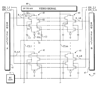
With reference to Fig. 5, a liquid crystal
display in accord with the present invention includes an
array 41 of picture cells 43, a first row selector 45, a
second row selector 47, a reference voltage generator 51
and preferably a single video signal generator 49.
Picture cells 43 are arranged into n rows and m columns.
First row selector 45 may independently control any of
the n rows by means of a first set of row select lines
ranging from R-1,A to R n,A. Similarly, second row
selector 47 may independently control the same n rows by
means of a second set of row select lines ranging from
R 1,B to R n,B.
Video signal generator 49 outputs m video
signals on m column lines ranging from CL1 to CLm. The
video signals preferably are within a voltage range of OV
through Vmax, of preferably 16V. Each column of picture
cells 43 is selected by means of a corresponding column
line, i.e. CL1. All picture cells 43 within a selected
column have an input node 52 coupled to a corresponding,
common column line, i.e. CL1. The video signal on a
column line CL1, however, is not accepted by all picture
cells 43 within the same column. Rather, only the
picture cells 43 that are activated by a row select line
from one of the first 45 or second 47 row selector will
latch in the video signal data on their respective column
line, CL1-CLm.
Each row within array 41 may be selected by any
one of a plurality of independent row selectors 45 and
47. Preferably no two row selectors 45, 47 may select
the same row at the same time. Any row, however, may be
selected by multiple row selectors 45, 47 in succession.
For example, in a first embodiment first row selector 45
may select the first row in array 41 by actuating row
select line R-1,A and thereby load image information from
video signal generator 49 onto the first row of picture
CA 02387749 2002-04-16
WO 01/35384 PCT/US00/25714
-10-
cells 43. During this time, no other selector, i.e.
second row selector 47, may access the first row. Once
first row selector 45 has relinquished use of the first
row, another row selector, i.e. second row selector 47,
may gain control of the fist row by actuating its
appropriate row select line, i.e. R 1,B.
Each picture cell 43 includes a liquid crystal
PXL and accompanying drive circuitry. The drive
circuitry selectively transfers a stored video signal
from a storage means C1 and C2 onto liquid crystal PXL.
The stored video signal is read from a corresponding
column line CL1-CLm. In the preferred embodiment, a
picture cell 43 may store multiple video signals while
simultaneously displaying another. To accomplish this,
each drive circuit within a picture cell 43 includes
multiple voltage storage devices. In the best mode
implementation, the multiple voltage storage devices are
implemented as a first storage capacitor C1 and a second
storage capacitor C2. This allows picture cell 43 to
display the contents of one storage capacitor, i.e. C1,
while storing new image information in another storage
capacitor, i.e. C2. It is to be understood that it is
likewise possible to store additional image information
by incorporating additional storage capacitors.
The input node 52 of each picture cell 43 may
be selectively coupled to one of storage capacitors C1
and C2 by means of a corresponding select transistor S1
and S2, respectively. Each of select transistors Sl and
S2 is controlled by a corresponding row select line R 1,A
and R-1,B controlled by a corresponding row selector 45
and 47. Similarly, a picture cell's storage capacitors
C1 and C2 may be selectively coupled to its liquid
crystal PXL by means of a corresponding enable transistor
E1 and E2, respectively. Each enable transistor E1 and
E2 is controlled by an independent enable signal EN 1,1
and EN-2,1. Enable signal EN 1,1 controls the coupling
CA 02387749 2002-04-16
WO 01/35384 PCT/US00/25714
-11-
of all the first storage capacitors C1 within row of a
picture cells 43 to each cell's respective liquid crystal
PXL. Similarly, enable signal EN 1,2 controls the
coupling of all the second storage capacitors C2 within a
row of picture cells 43 to each cell's respective liquid
crystal PXL. Thus, each row is responsive to a set of
enable signals EN_1,1/EN-2,1 that independently control
separate enable transistors within each picture cell 43.
In the preferred embodiment of Fig. 5, array 41
is responsive to n sets of such enable signal pairs
ranging from EN 1,1/EN 2,1 to EN l,n/EN 2,n. In this
preferred embodiment, however, all first enable
transistors E1 within array 41 are controlled by a common
first enable signal and all second enable transistors E2
are controlled by a second common enable signal. In this
manner, the contents of the first C1 and second C2
storage capacitors within each cell 43 of array 41 may be
transferred to their respective liquid crystal PXL in
unison.
Additionally, in this presently preferred
embodiment only one row selector 45 or 47 may control
array 41 at any given time. For example, first row
selector 45 may gain sole control of array 41 and
instigate sequential loading of a first image from video
signal generator 49 onto the whole of array 41 one row at
a time. After first row selector 45 finishes loading the
first image, it then relinquishes control of array 41 to
another row selector, i.e. 47. Once second row selector
47 gains control of array 41, it can begin transferring a
second image onto all the rows of array 41. While second
row selector 47 has control of array 41, the first enable
transistor S1 of each picture cell 43 within array 41
will be in an active state and coupling first storage
capacitor C1 to liquid crystal PXL while second enable
transistor 52 is in an inactive state.
CA 02387749 2002-04-16
WO 01/35384 PCT/US00/25714
-12-
As is known in the art, a voltage potential
applied to liquid crystal PXL modifies its reflectivity.
By appropriate application of voltage potentials to an
array's liquid crystals PXL, an image may be formed. In
the present embodiment, video signal generator 49
supplies the appropriate voltage potentials along column
lines CL1-CLm to a desired storage capacitor C1 or C2.
Since the video signals in the preferred embodiment may
vary between OV and a Vmax of 16V, this may result in a
high voltage stress across storage capacitors C1 and C2
if their lower plate is tide to ground. Therefore, the
presently preferred embodiment ties the lower plate of
storage capacitors C1 and C2 to reference voltage
generator 51, which supplies a voltage potential
intermediate OV and Vmax. Reference voltage generator 51
preferably supplies a voltage potential half-way between
both extreme voltage swings of video signal generator 49.
Presently, this means that reference voltage generator 51
supplies Vmax/2, or 8V, to the lower plate of all storage
capacitors within array 41. Consequently, although
select transistors S1 and S2 may transfer as little as OV
or as much as 16V onto the top plate of storage
capacitors C1 and C2, the voltage drop across storage
capacitors C1 and C2 remains within an 8V voltage swing.
As a result, storage capacitors C1 and C2 may be made
smaller and faster than otherwise required.
With reference to Fig. 6, a second embodiment
of the present invention is shown. All elements in Fig.
6 similar to those of Fig. 5 are given similar reference
characters and are explained above. In Fig. 6, all
picture cells 43 in array 41 share a common enable signal
ENBL which selectively couples one of storage capacitors
C1 and C2 to liquid crystal PXL. To accomplish this, the
enable transistors E and E B within each picture cell 43
respond oppositely to the logic state of enable signal
ENBL. First enable transistor E is an NMOS transistor
CA 02387749 2002-04-16
WO 01/35384 PCT/US00/25714
-13-
and responds to a logic high on signal ENBL by coupling
first storage capacitor C1 to liquid crystal PXL, and
responds to a logic low on signal ENBL by isolating C1
from PXL. Conversely, the second enable transistor E B
is a PMOS transistors and responds to a logic high on
ENBL by isolating C2 from PXL, and responds to a logic
low on ENBL by coupling second storage capacitor C2 to
PXL. Thus, liquid crystal PXL is constantly coupled to
one of either C1 and C2, as determined by enable signal
ENBL.
The embodiment of Fig. 6 is a specialized
variation of that of Fig. 5. In the second embodiment of
Fig. 6, only one of row selectors 45 and 47 may control
array 41 at a time. For example, if first row selector
45 has access to array 41, then second row selector 47
must wait until first row selector 45 finishes loading a
new image onto all of array 41, one row at a time. As
explained above, first row selector 45 accesses the first
storage capacitor C1 of a row of picture cells 43 by
actuating the first select transistor S1 within a row of
picture cells simultaneously. While first row selector
45 is loading image data into array 41, enable signal
ENBL is preferably at a logic low and isolating the first
storage capacitor C1 of all picture cells from their
respective liquid crystal PXL. A low on enable signal
ENBL also has the effect of coupling each cell's second
storage capacitor C2 to their respective liquid crystal
PXL. Thus, each picture cell 43 displays the contents of
its second storage capacitor C2 while it receives new
image data onto its first storage capacitor C1.
Once first row selector 45 has finished loading
the new image into array 41 and the new image is ready to
be displayed, enable signal ENBL is switched from a logic
low to a logic high. This activates first enable switch
E and deactivates second enable switch E B. The newly
loaded image information on first storage capacitors C1
CA 02387749 2002-04-16
WO 01/35384 PCT/US00/25714
-14-
is thereby coupled to its respective liquid crystals PXL
for display. Concurrently, second storage capacitor C2
is disconnected from the liquid crystal PXL. At this
point, second storage capacitor C2 is ready to receive
new data and second row selector 47 may take control of
array 41.
With reference to Fig. 7, a third embodiment of
the present invention is shown. All elements in Fig. 7
similar to those of Fig. 5 are given similar reference
characters and are explained above. The embodiment of
Fig. 7 shows multiple video signal generators 49A/49B and
preferably includes one signal generator 49A/49B for each
row selector 45 and 47, respectively. Each signal
generator 49A and 49B has its own set of column lines
CL1,A-CLm,A and CL1,B-CLm,B, respectively, by which each
has independent access to any column of picture cells 43
within array 41. Thus, each picture cell 43 includes a
separate input node 52A/52B per column line CL1,A/CL1,B,
respectively. A separate set of enable signals
EN-1,1/EN-2,1 independently controls the enable
transistors E1 and E2 of each row of picture cells 43 in
a manner similar to that of the first embodiment of the
first embodiment of Fig. 5.
In Fig. 7, multiple row selectors 45 and 47
have access to array 41 simultaneously, as was also the
case in the first embodiment of Fig. 5. Unlike the
structure of Fig. 5, however, the structure of Fig. 7
permits multiple row selectors 45 and 47 to access the
same row of picture cells 43 at the same time while
maintaining independent addressing of their respective
storage capacitors Cl and C2. For example assuming that
liquid crystal PXL has enough capacitance of its own to
maintain its current image data and that it is desired to
write to both of storage capacitors C1 and C2, then both
enable signals EN 1,l and EN 2,1 would be set to a logic
low. This would cause both enable transistors E1 and E2
CA 02387749 2002-04-16
WO 01/35384 PCT/US00/25714
-15-
to deactivate and isolate both C1 and C2 from their
respective liquid crystal PXL. It is to be understood
that if a picture cell 43 included a third storage
capacitor, then liquid crystal PXL could be maintained
coupled to the third storage capacitor while the first C1
and second C2 storage capacitors received new data.
While C1 is isolated from liquid crystal PXL, first row
selector 45 may activate row line R_1,A and thereby
activate first select transistor S1. This couples first
column line CL1,A from first video signal generator 49A
to first storage capacitor C1. Similarly, While C2 is
isolated from liquid crystal PXL, second row selector 47
may activate row line R 1,B and thereby activate second
select transistor S2. This couples second column line
CL1,B from second video signal generator 49B to second
storage capacitor C2. Since both storage capacitors C1
and C2 are coupled to separate column lines CL1,A and
CL1,B, respectively, they can both receive new data
simultaneously.