Note: Descriptions are shown in the official language in which they were submitted.
CA 02387910 2005-04-29
ELECTRODE FOR LITHIUM BATTERIES AND RECHARGEABLE LITHIUM
BATTERY
TECHNICAL FIELD
The present invention relates to a novel electrode for
use in lithium battery, a lithium battery and a rechargeable
lithium battery utilizing the electrode.
BACKGROUND ART
The battery performance of rechargeable lithium
batteries recently under intensive research and development,
such as charge-discharge voltage, cycle life characteristics
or storage characteristics, depends largely upon the types
of the electrodes used. This has led to the attempts to
better battery performance by improving electrode active
materials.
The use of metallic lithium for the negative active
material, although possible to construct a battery with high
energy density per weight and volume, presents a problem
that the lithium deposited on charge grows into dendrite
which could cause internal short-circuiting.
Rechargeable lithium batteries are reported (Solid
State Ionics, 113-115, p57 (1998)) which use an electrode
-1-
CA 02387910 2005-04-29
consisting of aluminum, silicon, tin or the like that is
electrochemically alloyed with lithium on charge. Among
these, a silicon electrode provides a particularly high
theoretical capacity and is promising as a high-capacity
negative electrode. For this reason, various rechargeable
batteries using silicon for the negative electrode are
proposed (Japanese Laid-Open Patent Application No. Hei 10-
255768). However, such alloying negative electrodes fail to
provide sufficient cycle characteristics since alloys, as
electrode active materials, are themselves pulverized on charge
and discharge to reduce current-collecting capabilities.
DISCLOSURE OF THE INVENTION
The inventors of this application have discovered that
an electrode including a thin film composed of active
material, such as a microcrystalline or amorphous silicon
thin film, deposited on a current collector by a thin film-
forming process such as a sputtering or CVD process exhibits
improved charge-discharge cycle characteristics when
incorporated in rechargeable lithium batteries, as
demonstrated in Reference Experiments-1 - 8 which will. be
later described.
They have also found the importance of adhesion between
the thin film of active material and the current collector
when satisfactory charge-discharge cycle characteristics are
-2-
CA 02387910 2002-04-18
pursued for such an electrode.
It is an object of the present invention to provide an
electrode for lithium batteries, in which a thin film of
active material capable of storage and release of lithium is
provided on a current collector and which can obtain the
improved charge-discharge cycle characteristics by the
enhanced adhesion of the thin film of active material to the
current collector.
The present invention is an electrode for lithium
batteries, in which a thin film of active material capable
of storage and release of lithium is provided on a current
collector through an interlayer and which is characterized
in that the interlayer comprises a material alloyable with
the thin film of active material.
The use of the interlayer that comprises a material
alloyable with the thin film of active material improves
adhesion of the thin film of active material to the current
collector. This construction prevents the thin film from
being separated from the current collector as it expands and
shrinks during a charge-discharge reaction, resulting in
obtaining improved charge-discharge cycling characteristics.
In one preferred embodiment in accordance with the
present invention, a metal or alloy foil which is higher in
mechanical strength than the interlayer material is used to
constitute the current collector.
-3-
CA 02387910 2006-08-17
In an aspect of the invention, there is provided an
electrode for a lithium battery, in which a film of active
material capable of storage and release of lithium is
provided, through an interlayer, on a current collector, the
electrode being characterized in that the interlayer comprises
a material alloyable with the film of active material, the
film of active material is divided into columns by gaps formed
therein, via a charge-discharge reaction thereof, in a manner
to extend in its thickness direction, and the columnar
portions are at their bottoms adhered to the interlayer,
wherein the interlayer is a copper layer.
In a further aspect of the invention, there is provided a
rechargeable lithium battery including a negative electrode
having a film of active material that is capable of storage
and release of lithium and deposited on a negative current
collector, a positive electrode and a nonaqueous electrolyte,
wherein an interlayer comprising a material alloyable with the
film of active material is provided on the negative current
collector, the film of active material is deposited on the
interlayer, the film of active material is divided into
columns by gaps formed therein, via a charge-discharge
reaction thereof, in a manner to extend in its thickness
direction, and the columnar portions are at their bottoms
adhered to the interlayer, wherein the interlayer is a copper
layer.
In another aspect of the invention, there is provided an
electrode for a lithium battery, in which a film of active
-3a-
CA 02387910 2006-08-17
material capable of storage and release of lithium is
provided, through an interlayer, on a current collector,
wherein the interlayer comprises a material alloyable with the
film of active material, the film of active material is
divided into columns by gaps formed therein in a manner to
extend in its thickness direction, and the columnar portions
are at their bottoms adhered to the interlayer, wherein the
interlayer is a copper layer.
In yet another aspect of the invention, there is provided
a rechargeable lithium battery including a negative electrode
having a film of active material that is capable of storage
and release of lithium and deposited on a negative current
collector, a positive electrode and a nonaqueous electrolyte,
wherein an interlayer comprising a material alloyable with the
film of active material is provided on the negative current
collector, the film of active material is deposited on the
interlayer, the film of active material is divided into
columns by gaps formed therein in a manner to extend in its
thickness direction, and the columnar portions are at their
bottoms adhered to the interlayer, wherein the interlayer is a
copper layer.
Another aspect of the invention provides an electrode for
a lithium battery, in which a film of active material capable
of storage and release of lithium is provided, through an
interlayer, on a current collector, wherein the interlayer
comprises a material alloyable with the film of active
material, a component of the interlayer is diffused into the
-3b-
CA 02387910 2006-08-17
film of active material, the film of active material is
divided into columns by gaps formed therein in a manner to
extend in its thickness direction, and the columnar portions
are at their bottoms adhered to the interlayer, wherein the
interlayer is a copper layer.
The invention also provides a rechargeable lithium
battery including a negative electrode having a film of active
material that is capable of storage and release of lithium and
deposited on a negative current collector, a positive
electrode and a nonaqueous electrolyte, wherein an interlayer
comprising a material alloyable with the film of active
material is provided on the negative current collector, the
film of active material is deposited on the interlayer, a
component of the interlayer is diffused into the film of
active material, the film of active material is divided into
columns by gaps formed therein in a manner to extend in its
thickness direction, and the columnar portions are at their
bottoms adhered to the interlayer, wherein the interlayer is a
copper layer.
-3c-
CA 02387910 2002-04-18
In the present invention, since the thin film of active
material expands and shrinks as it stores and releases
lithium, a stress is caused in the current collector during
a charge-discharge reaction. This stress causes formation
of wrinkles in the current collector as a result of
irreversible, that is, plastic deformation. This wrinkle
formation not only increases a volume of the battery but
also disturbs uniformity of an electrode reaction, resulting
in the reduction of an energy density. In order to suppress
formation of such wrinkles, the use of a material superior
in mechanical strength, such as in tensile strength and
tensile modulus, is preferred. However, if the thin film of
active material is deposited directly on such a material,
serving as a current collector, the adhesion therebetween
becomes occasionally insufficient to result in the failure
to obtain satisfactory charge-discharge cycling. In this
case, the interposition of the afore-stated interlayer
comprised of a material alloyable with the thin film of
active material between the current collector and the thin
film prevents separation of the thin film during the charge-
discharge reaction as well as suppresses formation of
wrinkles.
Accordingly, the use of a metal or alloy foil, which is
higher in mechanical strength than the interlayer material,
for the current collector is effective to suppress formation
-4-
CA 02387910 2002-04-18
of wrinkles in the current collector while maintaining
satisfactory charge-discharge cycling characteristics.
Also in the present invention, it is preferred that the
interlayer has irregularities on its surface. The presence
of such irregularities on the interlayer surface increases
an interfacial contact area between the interlayer and the
thin film of active material, resulting in the increased
adhesion between the thin film of active material and the
interlayer and thus between the thin film of active material
and the current collector.
These irregularities can be imparted onto the surface
of the interlayer, for example, by using the current
collector having surface irregularities. In this case, the
irregularities defined on the interlayer surface correspond
to those on the current collector.
In the above case, a surface roughness Ra (roughness
average) of the current collector is preferably in the range
of 0.001 - 1 pm, more preferably in the range of 0.01 - 1
pm. The surface roughness Ra is specified in Japanese
Industrial Standards (JIS B 0601-1994) and can be determined
by a surface roughness meter, for example.
In the present invention, the surface roughness Ra of
the current collector preferably satisfies the relationship
Ra t, where t is a thickness of the active material.
Also preferably, the surface roughness Ra of the current
-5-
CA 02387910 2002-04-18
collector and a mean spacing of local peaks of profile S
satisfy the relationship 10ORa ? S. The mean spacing of
local peaks of profile S is specified in Japanese Industrial
Standards (JIS B 0601-1994) and can be determined by a
surface roughness meter, for example.
The shape of projections of the irregularities on the
current collector surface is not particularly specified, but
may preferably be a conical form, for example.
In the present invention, the thin film of active
material can be formed from a material which can produce a
compound or solid solution with lithium, for example. Such
a material can be illustrated by at least one selected from
elements from Groups IIB, IIIB, IVB and VB of the periodic
table, and oxides and sulfides of transition metal elements
from Periods 4, 5 and 6 of the periodic table.
In the present invention, examples of elements from
Groups IIB, IIIB, IVB and VB of the periodic table that can
produce compounds or solid solutions with lithium include
carbon, aluminum, silicon, phosphorus, zinc, gallium,
germanium, arsenic, cadmium, indium, tin, antimony, mercury,
thallium, lead and bismuth. Specific examples of transition
metal elements from Periods 4, 5 and 6 of the periodic table
include scandium, titanium, vanadium, chromium, manganese,
iron, cobalt, nickel, copper, zinc, yttrium, zirconium,
niobium, molybdenum, technetium, ruthenium, rhodium,
-6-
CA 02387910 2002-04-18
palladium, silver, cadmium, lanthanum series elements,
hafnium, tantalum, tungsten, rhenium, osmium, iridium,
platinum, gold and mercury.
Preferred among the above-listed elements is at least
one selected from carbon, silicon, germanium, tin, lead,
aluminum, indium, zinc, cadmium, bismuth and mercury.
Silicon and/or germanium is more preferred.
In general, silicon is roughly classified by its
crystallinity into amorphous silicon, microcrystalline
silicon, polycrystalline silicon and single crystal silicon.
The term "noncrystalline silicon", as used herein, is meant
to encompass amorphous silicon and microcrystalline silicon
and exclude polycrystalline silicon and single crystal
silicon. Silicon is identified as the amorphous silicon
when Raman spectroscopy detects substantial absence of a
peak around 520 cm' which characterizes a crystalline
region, and as the microcrystalline silicon when Raman
spectroscopy detects the substantial presence of a peak
around 520 cm' which corresponds to the crystalline region
and a peak around 480 cm' which indicates an amorphous
region. Hence, the microcrystalline silicon consists
substantially of a crystalline region and an amorphous
region. Silicon is identified as the single crystal silicon
or polycrystalline silicon when Raman spectroscopy detects
the substantial absence of a peak around 480 cm' which
-7-
CA 02387910 2005-04-29
corresponds to the amorphous region.
In the present invention, a microcrystalline or
amorphous silicon thin film preferably serves as the thin
film of active material.
In addition to the above-described silicon thin film, a
germanium thin film or a silicon-germanium alloy thin film
may also be preferably used for the thin film of active
material in the present invention. The germanium thin film
in the amorphous or microcrystalline form is preferably
used. The preferred silicon-germanium alloy thin film has
the microcrystalline or amorphous form. The above-described
procedure applied to the silicon thin film can be similarly
utilized to determine the microcrystalline or amorphous
nature of the germanium and silicon-germanium alloy thin
films. The use of silicon and germanium provides good
results as evidenced by Examples which will be described
hereinafter. Since silicon and. germanium can be mixed with
each other in arbitrary proportions to produce solid
solutions, similar results are expected for the silicon-
germanium alloy.
In the case where a silicon, germanium or silicon-
germanium alloy thin film serves as the thin film of active
material, copper may be chosen as the material capable of
alloy formation therewith. It is accordingly preferred that
the interlayer is formed from copper when such thin films
-8-
CA 02387910 2005-04-29
are used. The tensile strength of copper is 212.7 N/mm2
(21.7 kgf/mm2, "Data Book of Metals, Revised 2nd Ed. ",
published by Maruzen Co.). A metal or alloy that has the
higher tensile strength than copper can be nickel
(tensile strength = 315.6 N/mm2 = 32.2 kgf/mm2, "Data
Book of Metals, Revised 2nd Ed. ", published by Maruzen
Co.) Accordingly, a nickel foil may preferably be used for
the current collector when copper forms the interlayer.
Other types of materials useful for the current collector
include copper alloys such as tin bronze (phosphor bronze),
silicon bronze and aluminum bronze, nickel alloys, iron and
iron alloys, and stainless steel. Molybdenum, tungsten and
tantalum can also be used to form the current collector.
In the present invention, the interlayer comprises a
material which is alloyable with the thin film of active
material. Preferably,- the interlayer component is allowed
to diffuse into the thin film of active material. The
diffusion of the interlayer component into the thin film of
active material not only improves adhesion between the
interlayer and the thin film of active material, but also
effectively prevents the thin film.of active material from
separating from the current collector. As a result, the
charge-discharge cycle characteristics are further improved.
In the case where the thin film is composed of active
material capable of alloy formation with lithium and the
-9-
CA 02387910 2005-04-29
interlayer comprising material incapable of alloy formation
with lithium is provided on the current collector, the .
diffusion of the interlayer component lessens expansion and
shrinkage of a thin film portion located in the vicinity of
the interlayer during storage and release of lithium. Thus,
the thin film of active material can be kept adhered more
effectively to the interlayer.
Preferably, a concentration of the interlayer component
in the thin film of active material is higher in the
vicinity of the interlayer and is lower at a location closer
to the surface of the thin film of active material. Due to
the presence of such a concentration gradient, expansion and
shrinkage of the thin film in the vicinity of the interlayer
is suppressed so that the thin film can be kept adhered to
the interlayer. Also, the thin film is allowed to contain a
relatively larger amount of active material in the vicinity
of its surface so that a high charge-discharge capacity is
assured.
It is preferred that the interlayer component, when
diffused in the thin film, forms a solid solution, instead
of an intermetallic compound, with a thin film component.
The intermetallic compound, as used herein, refers to a
compound which has a specific crystal structure formed via
combination of metals in specific proportions. The
formation of solid solution, instead of intermetallic
-10-
CA 02387910 2002-04-18
compound, between the thin film component and the interlayer
component improves adhesion between the thin film and the
interlayer, resulting in obtaining the increased charge-
discharge capacity.
The current collector preferably has a small thickness
and is preferably in the form of a metal foil. The current
collector is preferably composed of a material which does
not alloy with lithium. In the above-described case where
the interlayer is a copper layer, the current collector is
preferably comprised of a nickel foil.
When a nickel foil is used as the current collector, it
is possible to use a nickel foil having irregularities on
its surface, e.g., an electrolytic nickel foil.
The electrolytic nickel foil can be obtained, for
example, by immersing a metal drum in a liquid electrolyte
containing nickel ions dissolved therein, rotating the drum
and applying a current to the drum while being rotated so
that nickel is deposited on a surface of the drum, and then
removing the deposited nickel from the drum surface. Either
one or both sides of the electrolytic nickel foil may be
subjected to surface roughening or other surface treatment.
Alternatively, the nickel foil may be coated at its
surface with a surface-roughened copper layer by depositing
copper on a rolled nickel foil using an electrolytic
process.
-11-
CA 02387910 2002-04-18
In the present invention, it is preferred that the thin
film of active material is divided into columns by gaps
formed therein in a manner to extend in its thickness
direction and the columnar portions are at their bottoms
adhered closely to the interlayer. It is also preferred
that a thickness portion of the thin film that occupies at
least a half of its thickness is preferably divided into
columns by such gaps.
Preferably, the gaps are formed by the expansion and
shrinkage of the thin film, which may be caused to occur by
a charge-discharge reaction, for example. Accordingly, the
gaps may be formed by the charge-discharge reaction either
after or before the electrode is assembled into a battery.
Illustrating one possible method of forming such gaps in the
thin film of active material before it is subjected to a
charge-discharge process, the thin film of active material
in the electrode before being assembled into a battery is
allowed to store and then release lithium or the like so
that the thin film of active material undergoes expansion
and subsequent shrinkage in volume, thereby forming the
gaps. Alternatively, the thin film of active material may
be deposited in the form of distinct columns using a photo-
lithographically patterned resist film to provide the thin
film of active material that is divided by gaps into
columns.
-12-
CA 02387910 2002-04-18
In the case where the thin film of active material has
irregularities on its surface, the aforementioned gaps may
be formed therein to extend in a thickness direction from
valleys of the irregularities on the thin film surface
toward the current collector. The irregularities on the
thin film surface may be formed to correspond in shape to
those on the interlayer. That is, providing the interlayer
having surface irregularities and then depositing the thin
film of active material on the interlayer results in the
formation of the corresponding irregularities on the surface
of the thin film of active material.
The columnar portions of the thin film of active
material may have various top shapes, but preferably have a
round top shape.
The gaps may be formed in a thickness direction of the
thin film of active material along low-density regions
formed in advance therein. Such low-density regions may be
connected to each other like a network in a planar direction
and extend in the thickness direction toward the current
collector, for example.
In the present invention, the thin film of active
material can be deposited on the interlayer by various
methods, including, for example, CVD, sputtering, vapor
evaporation, spraying and plating processes. Particularly
preferred among such thin-film forming methods are CVD,
-13-
CA 02387910 2002-04-18
sputtering and vapor evaporation processes.
In the present invention, the thin film of active
material may be doped with an impurity. Examples of such
impurities include elements of the periodic Groups IIIB,
IVB, VB and VIB, such as phosphorus, aluminum, arsenic,
antimony, boron, gallium, indium, oxygen and nitrogen.
Also, the thin film of active material in the present
invention may be made up of a sequence of superimposed
layers. These layers may differ from each other in terms of
composition, crystallinity, impurity concentration or the
like. Such layers may provide a thin film structure graded
in its thickness direction. For example, such layers, if
properly arranged, can provide a thin film structure wherein
the composition, crystallinity, impurity concentration or
the like is varied in its thickness direction.
Preferably, the thin film of active material in the
present invention stores lithium via formation of an alloy
with lithium.
Lithium may be previously stored or incorporated in the
thin film of active material in the present invention.
Lithium may be added during deposition of the thin film of
active material. That is, lithium may be introduced via
formation of a lithium-containing thin film. Alternatively,
lithium may be added or stored after deposition of the thin
film of active material. One possible method is to use an
-14-
CA 02387910 2002-04-18
electrochemical mechanism whereby lithium is added or stored
in the thin film of active material.
The thickness of the thin film of active material in
the present invention is preferably 1 pm or above, for the
purpose of obtaining a high charge-discharge capacity.
In the present invention, the technique used to form
the interlayer on the current collector is not particularly
specified. Illustrative techniques include CVD, sputtering,
vapor evaporation, spraying and electrolytic (plating)
processes.
In the present invention, the thickness of the
interlayer is not particularly specified, so long as it is
sufficient to improve adhesion thereof to the thin film of
active material. The thickness is preferably in the range
of 0.01 - 10 pm, which range generally permits efficient
formation of the interlayer by the above-listed techniques.
The interlayer material is preferably compatible with
the current collector material and thus preferably alloyable
therewith.
The lithium battery of the present invention is
characterized as including a negative electrode comprised of
the above-described elecrode of the present invention, a
positive electrode and an electrolyte.
The term "lithium battery", as used herein, encompasses
a lithium primary battery and a lithium secondary battery.
-15-
CA 02387910 2002-04-18
Accordingly, the electrode of the present invention is
applicable to lithium primary batteries as well as to
lithium secondary batteries.
The rechargeable lithium battery (lithium secondary
battery) of the present invention is characterized as
including a negative electrode comprised of the above-
described elecrode of the present invention, a positive
electrode and a nonaqueous electrolyte.
An electrolyte solvent for use in the rechargeable
battery of the present invention is not particularly limited
in type but can be illustrated by a mixed solvent which
contains cyclic carbonate such as ethylene carbonate,
propylene carbonate or butylene carbonate and also contains
chain carbonate such as dimethyl carbonate, methyl ethyl
carbonate or diethyl carbonate. Also applicable is a mixed
solvent of the above-listed cyclic carbonate and an ether
solvent such as 1,2-dimethoxyethane or 1,2-diethoxyethane or
a chain ester such as y-butyrolactone, sulfolane or methyl
acetate. Illustrative electrolyte solutes are LiPF6, LiBF41
LiCF3SO3, LiN (CF3SO2) 2, LiN (C2F5SO2) 2, LiN (CF3SO2) (C4F9SO2) ,
LiC (CF3SO2) 3, LiC (C2F5SO2) 3, LiAsF6, LiC1O4, Li2B10Cllo, Li2B12C112
and mixtures thereof. Other applicable electrolytes include
a gelled polymer electrolyte comprised of an electrolyte
solution impregnated into a polymer electrolyte such as
polyethylene oxide, polyacrylonitrile or polyvinylidene
-16-
CA 02387910 2002-04-18
fluoride and inorganic solid electrolytes such as LiI and
Li3N, for example. The electrolyte for the recharageable
lithium battery of the present invention can be used without
limitation, so long as an Li compound as its solute that
imparts an ionic conductivity, as well as its solvent that
dissolves and retains the Li compound, remain undecomposed
at voltages during charge, discharge and storage of the
battery.
Examples of positive active materials for the present
invention include lithium-containing transition metal oxides
such as LiCoO2, LiNiO2, LiMn2O4, LiMnO2, LiCoo 5Ni0 502 and
LiNio 7Coo 2Mno 102; lithium-free metal oxides such as Mn02; and
the like. Other substances can also be used, without
limitation, if they are capable of electrochemical insersion
and release of lithium.
BRIEF DESCRIPTION OF THE DRAWINGS
Figure 1 is a schematic sectional view of a
rechargeable lithium battery fabricated in Reference
Examples;
Figure 2 is a photomicrograph (at a magnification of
2,000X) taken using a scanning electron microscope, showing
an electrode in Reference Example in its state before charge
and discharge;
Figure 3 is a photomicrograph (at a magnification of
-17-
CA 02387910 2002-04-18
5,000X) taken using a scanning electron microscope, showing
an electrode in Reference Example in its state before charge
and discharge;
Figure 4 is a photomicrograph (at a magnification of
500X) taken using a scanning electron microscope, showing an
electrode in Reference Example in its state after charges
and discharges;
Figure 5 is a photomicrograph (at a magnification of
2,500X) taken using a scanning electron microscope, showing
an electrode in Reference Example in its state after charges
and discharges;
Figure 6 is a photomicrograph (at a magnification of
1,000X) taken using a scanning electron microscope, showing
a silicon thin film of an electrode in Reference Example
when viewed from above;
Figure 7 is a photomicrograph (at a magnification of
5,000X) taken using a scanning electron microscope, showing
a silicon thin film of an electrode in Reference Example
when viewed from above;
Figure 8 is a photomicrograph (at a magnification of
1,000X) taken using a scanning electron microscope, showing
a silicon thin film of an electrode in Reference Example
when viewed from a slight angle;
Figure 9 is a photomicrograph (at a magnification of
5,000X) taken using a scanning electron microscope, showing
-18-
CA 02387910 2002-04-18
a silicon thin film of an electrode in Reference Example
when viewed from a slight angle;
Figure 10 is a schematic sectional view, showing a
silicon thin film in the process of being divided by gaps
into columns in Reference Examples;
Figure 11 a photomicrograph (at a magnification of
12,500X) taken using a transmission electron microscope,
showing a section of a silicon thin film of an electrode a3
in Reference Example;
Figure 12 a photomicrograph (at a magnification of
25,000X) taken using a transmission electron microscope,
showing a section of a silicon thin film of an electrode a6
in Reference Example;
Figure 13 is a diagrammatic representation of the
photomicrograph of Figure 11;
Figure 14 is a diagrammatic representation of the
photomicrograph of Figure 12;
Figure 15 is a photomicrograph (at a magnification of
1,000X) taken using a scanning electron microscope, showing
a silicon thin film surface of an electrode a3 in Reference
Example when viewed from above;
Figure 16 is a photomicrograph (at a magnification of
1,000X) taken using a scanning electron microscope, showing
a silicon thin film surface of an electrode a6 in Reference
Example when viewed from above;
-19-
CA 02387910 2002-04-18
Figure 17 is a graphical representation illustrating
concentration profiles of constituent elements in a silicon
thin film of an electrode a6 in Reference Example along the
depth of the film;
Figure 18 is a schematic view, showing a construction
of an apparatus which is employed when a thin film is formed
by a vacuum vapor evaporation technique in Reference
Examples;
Figure 19 is a photomicrograph (at a magnification of
2,000X) taken using a scanning electron microscope, showing
an electrode a7 in Reference Example in its state before
charge and discharge;
Figure 20 is a photomicrograph (at a magnification of
10,000X) taken using a scanning electron microscope, showing
the electrode a7 in Reference Example in its state before
charge and discharge;
Figure 21 is a photomicrograph (at a magnification of
2,000X) taken using a scanning electron microscope, showing
an electrode a8 in Reference Example in its state before
charge and discharge;
Figure 22 is a photomicrograph (at a magnification of
10,000X) taken using a scanning electron microscope, showing
the electrode a8 in Reference Example in its state before
charge and discharge;
Figure 23 is a photomicrograph (at a magnification of
-20-
CA 02387910 2002-04-18
500X) taken using a scanning electron microscope, showing
the electrode a7 in Reference Example in its state after
charges and discharges;
Figure 24 is a photomicrograph (at a magnification of
2,500X) taken using a scanning electron microscope, showing
the electrode a7 in Reference Example in its state after
charges and discharges;
Figure 25 is a photomicrograph (at a magnification of
500X) taken using a scanning electron microscope, showing
the electrode a8 in Reference Example in its state after
charges and discharges;
Figure 26 is a photomicrograph (at a magnification of
2,500X) taken using a scanning electron microscope, showing
the electrode a8 in Reference Example in its state after
charges and discharges;
Figure 27 is a photomicrograph (at a magnification of
1,000X) taken using a scanning electron microscope, showing
a germanium thin film of the electrode a7 in Reference
Example in its state after charges and discharges, when
viewed from above;
Figure 28 is a photomicrograph (at a magnification of
5,000X) taken using a scanning electron microscope, showing
a germanium thin film of the electrode a7 in Reference
Example in its state after charges and discharges, when
viewed from above;
-21-
CA 02387910 2002-04-18
Figure 29 is a photomicrograph (at a magnification of
1,000X) taken using a scanning electron microscope, showing
a germanium thin film of the electrode a7 in Reference
Example in its state after charges and discharges, when
viewed from a slight angle;
Figure 30 is a photomicrograph (at a magnification of
5,000X) taken using a scanning electron microscope, showing
a germanium thin film of the electrode a7 in Reference
Example in its state after charges and discharges, when
viewed from a slight angle;
Figure 31 is a photomicrograph (at a magnification of
1,000X) taken using a scanning electron microscope, showing
a germanium thin film of the electrode a8 in Reference
Example in its state after charges and discharges, when
viewed from above;
Figure 32 is a photomicrograph (at a magnification of
5,000X) taken using a scanning electron microscope, showing
a germanium thin film of the electrode a8 in Reference
Example in its state after charges and discharges, when
viewed from above;
Figure 33 is a photomicrograph (at a magnification of
1,000X) taken using a scanning electron microscope, showing
a germanium thin film of the electrode a8 in Reference
Example in its state after charges and discharges, when
viewed from a slight angle;
-22-
CA 02387910 2002-04-18
Figure 34 is a photomicrograph (at a magnification of
5,000X) taken using a scanning electron microscope, showing
a germanium thin film of the electrode a8 in Reference
Example in its state after charges and discharges, when
viewed from a slight angle;
Figure 35 is a photomicrograph (at a magnification of
1,000X) taken using a scanning electron microscope, showing
a germanium thin film of the electrode a7 in Reference
Example in its state before charge and discharge, when
viewed from above;
Figure 36 is a photomicrograph (at a magnification of
1,000X) taken using a scanning electron microscope, showing
a germanium thin film of the electrode a8 in Reference
Example in its state before charge and discharge, when
viewed from above;
Figure 37 is a graphical representation illustrating
concentration profiles of constituent elements in a
germanium thin film of the electrode a7 in Reference Example
along the depth of the film;
Figure 38 is a graphical representation, illustrating
concentration profiles of constituent elements in a
germanium thin film in the electrode a8 in Reference Example
along the depth of the film;
Figure 39 is a photomicrograph (at a magnification of
2,000X) taken using a scanning electron microscope, showing
-23-
CA 02387910 2002-04-18
a section of an electrode a-11 in Reference Example before
charge and discharge;
Figure 40 is a photomicrograph (at a magnification of
10,000X) taken using a scanning electron microscope, showing
a section of the electrode a-11 in Reference Example before
charge and discharge;
Figure 41 is a photomicrograph (at a magnification of
1,000X) taken using a scanning electron microscope, showing
a silicon thin film of the electrode a-l1 in Reference
Example before charge and discharge, when viewed from above;
Figure 42 is a photomicrograph (at a magnification of
1,000X) taken using a scanning electron microscope, showing,
a silicon thin film of the electrode a-11 in Reference
Example after charges and discharges, when viewed from
above;
Figure 43 is a photomicrograph (at a magnification of
500,000X) taken using a transmission electron microscope,
showing an interface between a copper foil and a silicon
thin film and its vicinities;
Figure 44 is a photomicrograph (at a magnification of
1,000,000X) taken using a transmission electron microscope,
showing an interface between a copper foil and a silicon
thin film and its vicinities;
Figure 45 is a graphical representation, illustrating
concentration profiles of copper and hydrogen in a mixed
-24-
CA 02387910 2005-04-29
layer in an electrode cl along the depth of the layer; and
Figure 46 is a graphical representation, illustrating
concentration profiles of copper and hydrogen in a mixed
layer in an electrode c3 along the depth of the layer.
Figure 47 graphically shows evaluation results for
charge-discharge cycle characteristics in the Experiment A
in accordance with the present invention.
BEST MODE FOR CARRYING OUT THE INVENTION
The present invention is below described in more detail
by way of examples. It will be recognized that the
following examples merely illustrate the practice of the
present invention but are not intended to be limiting
thereof. Suitable changes and modifications can be effected
without departing from the scope of the present invention.
The following Reference Experiments 1 - 8 demonstrate
that a microcrystalline silicon thin film, an amorphous
silicon thin film and an amorphous germanium thin film, each
formed on a current collector such as a copper foil by a CVD
or sputtering process, provide good charge-discharge cycle
characteristics when they are used for the electrode for
rechargeable lithium batteries.
REFERENCE EXPERIMENT 1
Fabrication of Negative Electrode
A microcrystalline silicon thin film was formed on a
-25-
CA 02387910 2002-04-18
rolled copper foil (18 pm thick) by a CVD method, using the
rolled copper foil as a substrate, silane (SiH4) as a source
gas and a hydrogen gas as a carrier gas. Specifically, the
copper foil as a substrate was placed on a heater within a
reaction chamber. An interior of the reaction chamber was
evacuated by a vacuum evacuator to a pressure of 1 Pa or
lower. The silane gas as a source gas and the hydrogen (H2)
gas as a carrier gas were introduced via a source gas inlet
port. The substrate was heated to 180 C on the heater. A
degree of vacuum was adjusted by the vacuum pumping
apparatus to a reaction pressure. An RF power supply was
operated to excite a radio frequency wave which is
introduced via an electrode to induce a glow discharge.
Detailed thin-film forming conditions are listed in Table 1.
In Table 1, a volumetric unit, sccm, indicates a volumetric
flow rate (cm3/minute) of a fluid at 0 C at 1 atmospheric
pressure (101.33 kPa) per minute and is an abbreviation of
standard cubic centimeters per minute.
Table 1
Conditions 11 During Film Formation
Source Gas (SiH4) Flow Rate l0sccm
Carrier Gas (H2) Flow Rate 200sccm
Substrate Temperature 180 C
Reaction Pressure 40Pa
RF Power 555W
-26-
CA 02387910 2005-04-29
The microcrystalline silicon thin film was deposited
under the above-specified conditions to a thickness of about
pm. Observation by an electron microscope (at 2,000,OOOX
magnification) ascertained noncrystallinity of the thin film
5 in the way that an amorphous region was arranged to surround
a crystalline region consisting of microfine crystal. grains.
A 17 nun diameter piece was punched out from the resulting
sample to provide an electrode al. A piece identical to the
electrode al was subjected to heat treatment at 400 C for 3
10 hours to provide an electrode a2.
For comparative purposes, 90 parts by weight of
commercially available single crystal silicon powder
(particle diameter of 10 um) and 10 parts by weight of
polytetrafluoroethylene as a binder were mixed. This
mixture was pressed in a 17 mm diameter mold to obtain a
pellet-form electrode bl.
Fabrication of Positive Electrode
Starting materials, Li2CO3 and CoCO31 were weighed such
that the atomic ratio of Li and Co, Li:Co, was brought to
1:1, and then mixed in a mortar. The mixture was pressed in
a 17 mm diameter mold and calcined in the air at 800 C for
24 hours to obtain a calcined product consisting of LiCoO2.
This was subsequently ground into particles with a mean
particle diameter of 20 pm.
80 parts by weight of the resulting LiCoO2 powder, 10
-27-
CA 02387910 2005-04-29
parts by weight of acetylene black as a conducting material
and 10 parts by weight of polytetrafluoroethylene as a
binder were mixed. The mixture was pressed in a 17 mm
diameter mold to obtain a pellet-form positive electrode.
Preparation of Electrolyte Solution
1 mole/liter of LiPF6 was dissolved in a mixed solvent
containing equal volumes of ethylene carbonate and diethyl
carbonate to prepare an electrolyte solution for use in the
following battery construction.
Construction of Battery.
A coin type rechargeable lithium battery was
constructed using the above-fabricated electrode al, a2 or
bl for the negative electrode, and the above-fabricated
positive electrode and the above-prepared electrolyte
solution.
Figure 1 is a schematic sectional view, illustrating a
such-constructed rechargeable lithium battery which includes
a positive electrode 1, a negative electrode 2, a separator
3, a positive can 4, a negative can 5, a positive current
collector 6, a negative current collector 7 and an
insulating gasket 8 made of polypropylene.
The positive electrode 1 and negative electrode 2 are
disposed on opposite sides of the separator 3. These are
enclosed in a battery case composed of the positive can 4
and negative can 5. The positive electrode .1 is connected
-28-
CA 02387910 2005-04-29
to the positive can 4 by the positive current collector 6.
The negative electrode 2`is connected to the negative can 5
by the negative current collector 7. Such construction
enables charge and discharge as a secondary battery.
As a result, batteries Al, A2 and B1 were constructed
using the electrodes al, a2 and bl for the negative
electrode, respectively.
Measurement of Charge-Discharge Cycle Life
Characteristics
Each battery, excepting the battery Bl, was charged at
a current of 100 ~iA at 25 C until a negative electrode
capacity reached 2,000 mAh/g, and then discharged. This was
recorded as a unit charge-discharge cycle. Cycling was
effected to measure a 50th-cycle capacity retention rate for
each battery. The battery B1, which could not be charged to
2,000 mAh/g, was subjected to a cycle test wherein it was
charged to 4.2 V and then discharged. The results are given
in Table 2.
In Table 2, a hydrogen concentration obtained from SIMS
measurement, a ratio of peak intensities around 480 cm-1 and
520 cm-1 as determined by Raman spectral analysis, and a
crystal grain size calculated from an X-ray diffraction
spectrum and the Scherrer's equation, all for the negative
active material of each battery, are also given. Also, the
crystal grain size of the negative active material of the
-29-
CA 02387910 2006-08-17
battery Bl is given by the particle diameter of the powder
since both are considered to be almost equal in value to
each other.
Table 2
50th-Cycle Ratio of Peak
Battery Capacity Hydrogen Intensities Crystal
Retention Content (480cm1/520cm1) Grain Size
Rate (atomic%)
Al 85% 4 0.1 lnm
A2 78% 0.01 0.1 lnm
Bl 5% 0 0 10pm
As can be clearly seen from the results shown in Table
2, the batteries Al and A2 in accordance with the present
invention both exhibit markedly higher capacity retention
rates compared to the comparative battery B1.
As such, the use of the microcrystalline silicon thin
film for the negative active material results in the marked
improvement of charge-discharge cycle characteristics of the
rechargeable lithium battery. This is believed due to the
following reason: In the microcrystalline silicon thin
film, the moderation of expansion and shrinkage which occurs
when lithium is stored and released prevents the negative
active material from being pulverized and thereby suppresses
the possible reduction of current collecting capability.
(REFERENCE EXPERIMENT 2)
The procedure used in Reference Experiment 1 to
-30-
CA 02387910 2005-04-29
construct the battery Al was followed, except that an
electrolytic copper foil (18 pm thick) was used for the
current collector as a substrate. That is, a
microcrystalline silicon thin film (about 10 dun thick) was
deposited on the electrolytic copper foil to fabricate an
electrode a3. Using this electrode, a battery A3 was
constructed.
Also, the rolled copper foil used in Reference
Experiment 1 was subjected to a one-minute grinding treatment
with a #400 or #120 emery paper to provide a ground copper
foil. The procedure used in Reference Experiment 1 to
construct the battery Al was followed, except that such a
ground copper foil was used for the current collector as a
substrate. That is, a microcrystalline silicon thin film
(about 10 dun thick) was deposited on the copper foil to
fabricate an electrode. The electrode fabricated using the
copper foil ground with a #400 emery paper was designated as
an electrode a4 and the electrode fabricated using the
copper foil ground with a #120 emery paper was designated as
an electrode a5. These electrodes were used to construct
batteries A4 and AS in the same manner as in Reference
Experiment 1.
These batteries A3 - A5 and the batteries Al and B1
constructed in Reference Experiment 1 were subjected to a
charge-discharge cycle test under the same conditions used
-31-
CA 02387910 2002-04-18
in Reference Experiment 1 to obtain a 10th-cycle capacity
retention rate for each. The results are given in Table 3.
Also given in Table 3 are a surface roughness Ra and a mean
spacing of local peaks S for the copper foil, as a current
collector, of each of the batteries Al, B1 and A3 - A5.
The surface roughness Ra and the mean spacing of local
peaks S for each copper foil were measured using a stylus
profiler Dektak ST (available from ULVAC Inc.) with a
scanning distance of 2.0 mm. The surface roughness Ra was
calculated after correction of a deflection portion. The
deflection portion was collected using the correction values
with a low pass = 200 pm and a high pass = 20 pm. The
surface roughness Ra was automatically calculated and the
mean spacing of local peaks S was read from the chart.
Table 3
10th-Cycle Current Collector (Copper Foil)
Battery Capacity
Retention Surface Roughness Ra Mean Spacing S
Rate (pm) (pm)
Al 97% 0.037 14
A3 99% 0.188 11
A4 98% 0.184 9
A5 99% 0.223 8
B1 20% 0.037 14
As can be clearly seen from the results given in Table
3, the batteries A3 - AS using the copper foils with higher
-32-
CA 02387910 2005-04-29
values of surface roughness Ra for the-current collector
exhibit improved 10th-cycle capacity retention rates
compared to the battery Al using the copper foil with the
lowest value of surface roughness Ra. This is considered
due to the following reason: The copper foil with a higher
value of surface roughness Ra, when used for the current
collector, improves adhesion between the current collector
and the active material. This adhesion improvement reduces
the influence of structural change, such as falling-off of
the active material that occurs when it expands or shrinks
during storage or release of lithium.
REFERENCE EXPERIMENT 3
The batteries Al and A3 respectively constructed in
Reference Experiments 1 and 2 were further subjected to a
charge-discharge cycle test under the same test conditions
as used in the Reference Experiment 1 to measure a 30th
cycle capacity retention rate. The results are shown in
Table 4.
Table 4
Battery 30th-Cycle Capacity Retention Rate
Al 91%
A3 97%
As can be clearly seen from the results given in Table
4, the batteries Al and A3 exhibit good capacity retention
-33-
CA 02387910 2005-04-29
rates even on the 30th-cycle. Particularly, the battery A3
using the copper foil with a higher value of surface
roughness Ra for the current collector exhibits good
capacity retention rate.
The electrode a3 incorporated in the battery A3 was
viewed under an electron microscope to observe a condition
of its silicon thin film. First, the electrode a3 in its
state prior to being incorporated in the battery, i.e.,
before charge and discharge, was observed using a scanning
electron microscope. Figures 2 and 3 are photomicrographs
(secondary electron images) taken with a scanning electron
microscope, both showing the electrode a3 in its state
before charge and discharge. Figures 2 and 3 are taken at
2,000X and 5,000X magnifications, respectively.
The electrode was embedded in a resin and then sliced
to provide a sample. The layers of the embedding resin are
found in upper and lower end portions of Figure 2 and in an
upper end portion of Figure 3.
In Figures 2 and 3, a portion that appears slightly
lighter indicates the copper foil. The deposited silicon thin
film (about 10 }un thick) is found as a dark portion on the
copper foil. As shown in Figures 2 and 3, irregularities
are formed on a surface of the copper foil. Particularly,
projections have a generally conical shape. Similar
irregularities are formed on a surface of the silicon thin
-34-
CA 02387910 2002-04-18
film deposited on the copper foil. Accordingly, the surface
irregularities of the silicon thin film appear to generally
conform in shape to those formed on the copper foil surface.
Next, the electrode a3 was removed from the battery A3
after 30 cycles, embedded in a resin, and then subjected to
observation under a scanning electron microscope in the same
manner as described previously. Here, the electrode a3 was
removed after discharge. Thus, the observed electrode a3
was in its state after discharge.
Figures 4 and 5 are photomicrographs (secondary
electron images) taken with a scanning electron microscope,
each showing the electrode a3 after discharge. Figures 4
and 5 are taken at 500X and 2,500X magnifications,
respectively.
As shown in Figures 4 and 5, the silicon thin film has
gaps that extend in its thickness direction and divide the
silicon thin film into columns. Gaps are barely found to
extend in a planar direction. A bottom of each columnar
portion is found to adhere well to the copper foil as a
current collector. Also, each columnar portion has a round
top. It is thus understood that these gaps are formed to
originate from the valleys of irregularities that were found
on the surface of the silicon thin film in its state before
charge and discharge.
Further, the surface of the silicon thin film of the
-35-
CA 02387910 2002-04-18
electrode a3 after charges and discharges was observed with
a scanning electron microscope. Figures 6 and 7 are
photomicrographs (secondary electron images) taken with a
scanning electron microscope, each showing the surface of
the silicon thin film when viewed from above. Figures 6 and
7 are taken at 1,000X and 5,000X magnifications,
respectively. Figures 8 and 9 are photomicrographs
(secondary electron images) taken with a scanning electron
microscope, each showing the surface of the silicon thin
film when viewed at a slight angle. Figures 8 and 9 are
taken at 1,000X and 5,000X magnifications, respectively.
As shown in Figures 6 - 9, the gaps are formed in such
a way to surround the columnar portions of the silicon thin
film so that spaces are defined between neighboring columnar
portions. When the silicon thin film stores lithium on
charge, the columnar portions will expand and increase in
volume. This increment in volume, however, is believed to
be accommodated by those spaces provided around the columnar
portions. On discharge, the columnar portions of the
silicon thin film release the lithium and shrink to decrease
in volume. This decrement in volume is believed to restore
the spaces around the columnar portions. Such a columnar
structure of the silicon thin film is effective to relax a
stress caused by expansion and shrinkage of the active
material on charge and discharge, so that falling-off of the
-36-
CA 02387910 2005-04-29
active silicon thin film from the current collector can be
prevented.
The formation of the gaps which divide the silicon thin
film into columns results in a marked increase in contact
area thereof with the electrolyte solution. Also, the
columnar portions are almost comparable in size to each
other. These are believed to allow efficient occurrence of
a charge-discharge reaction accompanying storage and release
of lithium in the thin film of active material.
Since the individual columnar portions of the silicon
thin film adhere to the current collector, as shown in
Figures 4 and 5, good electrical connection is provided
between the active material and the current collector. This
is believed to allow efficient occurrence of the charge-
recharge reaction.
As also shown in Figures 6 - 9, each columnar portion
has a round top. This provides an electrode structure which
prevents localized current concentration and reduces the
occurrence such as of a deposition reaction of a lithium
metal.
Figure 10 is a schematic sectional view, illustrating a
process whereby the silicon thin film deposited on a copper
foil is divided into columns by the gaps formed therein.
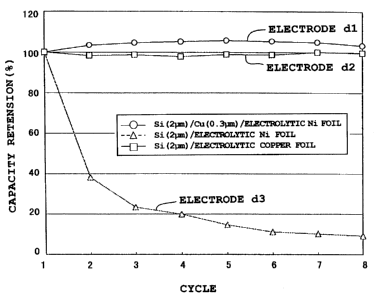
As shown in Figure 10(a), the copper foil 10 has
irregularities on its surface 10a. The copper foil with the
-37-
CA 02387910 2002-04-18
increased value for surface roughness Ra has the larger
irregularities.
Figure 10(b) illustrates a noncrystalline silicon thin
layer 11 deposited on a rough surface 10a of the copper foil
10. The surface lla of the silicon thin film 11 is
influenced by the irregularities on the surface l0a of the
copper foil 10 to have similar irregularities. Before
charge and discharge, the silicon thin film 11 remains
undivided, as shown in Figure 10 (b) . When charging is
effected, the silicon thin film 11 stores lithium therein
and expands in volume. During the charge, the silicon thin
film 11 appears to expand in both thickness and planar
directions of the thin film, although the detail is not
clear. During the subsequent discharge reaction, the
silicon thin film 11 releases lithium therefrom and shrinks
in volume. At this time, a tensile stress is produced in
the silicon thin film 11. Probably, such a stress
concentrates at valleys lib of the irregularities on the
surface lla of the silicon thin film 11 to result in the
formation of gaps 12 that originate from the valleys llb and
extend in the thickness direction, as shown in Figure 1.0(c)
Conceivably, the gaps 12 such formed relax the stress to
allow the silicon thin film 11 to shrink without occurrence
of falling-off from the copper foil 10.
In the silicon thin film divided into columns in the
-38-
CA 02387910 2002-04-18
fashion as described above, the spaces provided around the
columnar portions serve to relax the stress resulting from
expansion and shrinkage of the active material during the
succeeding charge-discharge cycles. This appears to assure
repetitive charge-discharge cycling while preventing
falling-off of the active material from the current
collector.
Further, the electrode a3 incorporating an about 1.0 pm
thick, microcrystalline silicon thin film deposited on an
electrolytic copper foil was observed under a transmission
electron microscope to study a mechanism whereby the gaps
are formed in the silicon thin film. Figure 11. is a
photomicrograph (at a magnification of 12,500X) taken with a
transmission electron microscope, showing a section of the
electrode a3-before charge and discharge. The observation
sample was prepared by slicing the resin-embedded electrode.
Figure 13 is a diagrammatic representation of the
photomicrograph of Figure 11. In the photomicrograph of
Figure 11 taken with a transmission electron microscope, the
silicon thin film 11 is deposited on the surface 10a of the
electrolytic copper foil 10, as diagrammatically shown in
Figure 13. The silicon thin film 11 appears light relative
to the copper foil 10 in the photomicrograph taken with a
transmission electron microscope. In the silicon thin film
shown in Figure 11, light portions are observed in the
-39-
CA 02387910 2002-04-18
regions extending between respective valleys lib and 10b of
the irregularities on the surfaces lla and 10a of the
silicon thin film 11 and copper foil 10. These light
portions are indicated by single-dotted chain lines A, B and
C in Figure 13. Particularly, the light portion is observed
more clearly in the region indicated by A. These regions
are considered to be low in density, i.e., low-density
regions of the silicon thin film 11. For the purpose of
observing such low-density regions in more detail, an
electrode a6 was fabricated by depositing an about 2 pm
thick, microcrystalline silicon thin film on an electrolytic
copper foil under the same conditions as used in the
fabrication of the electrode a3.
Figure 12 is a photomicrograph taken by a transmission
electron microscope, showing the electrode a6 when observed
in the same manner as described above. Figure 12 is taken
at a magnification of 25,000X. Figure 14 is a diagrammatic
representation of the photomicrograph of Figure 12. As
clear from Figure 12, a low-density region is also observed
in the region D of the electrode a6 that extends between the
respective valleys llb, 10b of the irregularities on the
surfaces lla, 10a of the silicon thin film 11 and the copper
foil 10. A detailed observation of the photomicrograph of
Figure 12 reveals a number of fine lines extending in
directions shown by the arrows in Figure 14. It seems very
-40-
CA 02387910 2002-04-18
likely that such lines are formed as the silicon thin film
grows. It accordingly appears that the silicon thin film 11
grows generally perpendicularly to the surface 10a of the
copper foil 10. It also appears that the silicon thin film
layer grows in such a direction to collide at the region D
with an adjacent silicon thin film layer being deposited and
growing on the adjacent inclined surface of the copper foil.
Thus the formation of the low-density region D is very
likely to have resulted from such a collision at the region
D. It also appears that the collision of the silicon thin
film layers with each other is continued till the end of
thin film formation, and formation of the low-density region
also continues until reaching the surface of the silicon
thin film.
Figure 15 is a photomicrograph (secondary electron
image) taken with a scanning electron microscope, showing a
surface of a silicon thin film of an electrode a3 when
observed from above. The electrode a3 shown in Figure 15 is
in its state before charge and discharge. Figure 15 is
viewed at 1,000X magnification. In Figure 15, portions
appearing lightened indicate projections on a surface of the
silicon thin film and the surrounding portions appearing
darkened indicate valleys on the surface of the silicon. thin
film. As shown in Figure 15, the valleys on the surface of
the silicon thin film are connected to each other like a
-41-
CA 02387910 2002-04-18
network. It is accordingly found that the low-density
regions define a continuous network in a plane of the
silicon thin film. As shown in Figures 11 and 13, such a
reticulated low-density region also extends in a thickness
direction toward the current collector. The dark portions
in Figure 15 do not indicate the gaps (spaces). This is
apparent from the fact that no gap (space) is observed which
extends in the thickness direction of the thin film in the
photomicrographs of Figures 2 and 3 taken by a scanning
electron microscope.
Figure 16 is a photomicrograph (secondary electron
image) taken at a magnification of 1,000 using a scanning
electron microscope, showing a surface of a silicon thin
film, when observed from above, of an electrode a6 in its
state before charge and discharge. As apparent from Figure
16, the valleys in the electrode a6 are also connected to
each other like a network. It is accordingly found that the
low-density regions are arranged like a network continuous
in a planar direction.
Figure 17 is a graph showing concentration profiles of
constituent elements along the thickness of the silicon thin
film in the electrode a6. The concentration profiles of
constituent elements were obtained via measurement of
concentrations of copper (63Cu) and silicon (Si2+) by SIMS
using 02+ as a sputtering source. In Figure 17, the abscissa
-42-
CA 02387910 2005-04-29
indicates a depth (}im) from a surface of the silicon thin
film and the ordinate indicates an intensity (count) of each
consituent element.
As apparent from Figure 17, a constituent element of
the current collector, copper (Cu), is found to diffuse in
the silicon thin film at locations adjacent to the current
collector. The copper (Cu) concentration decreases at a
location closer to the surface of the silicon thin film.
The copper (Cu) concentration is also found to vary in a
continuous fashion. This demonstrates that a solid solution
of silicon and copper, instead of an intermetallic compound
thereof, is formed in the copper(Cu)-diffused region.
In view of the previous discussion, the following is
very likely to explain a mechanism whereby the gaps are
formed in the silicon thin film to extend in its thickness
direction as it expands and shrinks during charge and
discharge. That is, a stress caused by expansion or
shrinkage in volume of the silicon thin film concentrates at
valleys of the irregularities on the silicon thin film
surface, as previously explained by referring to Figure 10.
Also, in the silicon thin film, there initially exists low-
density regions which are relatively low in mechanical
strength, extending from the valleys toward the current
collector. As the result of the above-mentioned situations,
the gaps (spaces) are likely to be formed along these low-
-43-
CA 02387910 2002-04-18
density regions.
Also, as shown in Figure 17, the diffusion of copper, a
constituent element of the current collector, into the
silicon thin film creates a concentration gradient of copper
therein, so that the copper concentration is higher at a
location closer to the current collector and lower at a
location closer to the surface of the silicon thin film.
Accordingly, a higher concentration of copper nonreactive
with lithium and a lower concentration of silicon reactive
with lithium exist at a location closer to the current
collector. In the vicinity of the current collector, the
silicon thin film is believed to store and release less
lithium, undergo less expansion and shrinkage, and thus
produce a lower level of stress which leads to the reduced
formation of the gaps (spaces) which may occasion separation
or removal of the silicon thin film from the current
collector. As a result, the bottoms of the columnar
portions of the silicon thin film can be kept adherent to
the current collector.
The silicon thin film divided by such gaps into columns
keeps a strong adhesion to the current collector even during
charge-discharge cycles. Also, the spaces provided to
surround the columnar portions serve to relax the stress
caused by expansion and shrinkage of the thin film that
occur with charge-discharge cycling. These are believed to
-44-
CA 02387910 2005-04-29
be contributors to excellent charge-discharge cycle
characteristics.
REFERENCE EXPERIMENT 4
Fabrication of Electrode a7
An electrolytic copper foil similar to that for use in
the fabrication of the electrode a3 was used for a current
collector as a substrate. An amorphous germanium thin film
(about 2 dun thick) was formed on this copper foil by an RF
sputtering technique to fabricate an electrode' a7.
The thin film was formed using germanium as a target,
at a sputtering gas (Ar) flow rate of 100 sccm, an ambient
substrate temperature (not heated), a reaction pressure of
0.1 Pa, and 200 W RF power.
The resulting germanium thin film was analyzed by Raman
spectroscopy which detected the presence of a peak around
274 cm-1 and the absence of a peak around 300 cm-1. This
revealed an amorphous nature of the germanium thin film.
Fabrication of Electrode a8
An amorphous germanium thin film (about 2,pm thick) was
formed on an electrolytic copper foil, similar in type to
the current collector of the electrode a7, by using a vapor
evaporation technique to fabricate an electrode a8.
Specifically, the germanium thin film was deposited on
the substrate by utilizing an apparatus of the construction
shown in Figure 18. Referring to Figure 18, an ECR plasma
-45-
CA 02387910 2005-04-29
source 21 includes a plasma generation chamber 22 to' which a
microwave power 25 and an Ar gas 26 are supplied. An Ar
plasma is generated when the microwave power 25 is supplied
to the plasma generation chamber 22. This Ar plasma 23 is
directed to exit from the plasma generation chamber 22 and
bombard a substrate 20. The germanium thin film can be
deposited on the substrate 20 by utilizing an electron beam
from an electron beam (EB) gun disposed below the substrate
20.
The electrolytic copper foil substrate was pretreated
by Ar plasma irradiation before the germanium thin film was
deposited thereon. A degree of vacuum within the reaction
chamber was adjusted to about 0.05 Pa (about 5 x 10⁻⁴ Torr).
The substrate was exposed to the Ar plasma under conditions
of an Ar gas flow rate of 40 sccm and a supplied microwave
power of 200 W. During the Ar plasma irradiation, a bias
voltage of -100 V was applied to the substrate. The
pretreatment was accomplished by exposing the substrate to
the Ar plasma for 15 minutes.
Next, the germanium thin film was deposited at a
0
deposition rate of 1 nm/sec (10 A/sec) using an electron
beam gun. The substrate temperature was ambient temperature
(not heated).
The resulting germanium thin film was analyzed by Raman
spectroscopy which revealed an amorphous nature of the
-46-
CA 02387910 2005-04-29
germanium thin film, as similar to the electrode a7.
Fabrication of Electrode b2
80 parts by weight of germanium powder with a mean
particle diameter of 10 pm, 10 parts by weight of acetylene
black as an electroconductive material, and 10 parts by
weight of polytetrafluoroethylene as a binder were mixed.
This mixture was pressed in a 17 mm diameter mold to
fabricate a pellet-form electrode b2.
Construction of Batteries
The procedure of Experiment was repeated, except that
the above-fabricated electrodes a7, a8 and b2 were used for
the negative electrode, to construct batteries A7, AS and
B2.
Evaluation of Charge-Discharge Cycle Characteristics
Each battery was charged at a current of 0.1 mA at 25
C to 4.2 V, and then discharged to 2.75 V. This standard
charge-discharge cycling was repeated to measure a capacity
retention rate on the 10th cycle. The measurement results
are given in Table S.
Table 5
Battery 10th-Cycle Capacity Retention Rate
A7 96%
A8 93%
B2 39%
-47-
CA 02387910 2005-04-29
As apparent from Table 5, the batteries A7 and AS using
the electrodes in accordance with this invention, i.e., the
electrodes incorporating the germanium thin film formed on
the current collector, for the negative electrode exhibit
markedly improved capacity retention rates compared to the
battery B2 using the germanium powder for the negative
electrode.
Observation With Electron Microscope
Figures 19 and 20 are photomicrographs (reflection
electron images) taken with a scanning electron microscope,
each showing a section of the electrode a7 in its state
before being charged and discharged. Figures 19 and 20 were
taken at magnifications of 2,000X and 10,000X, respectively.
Each electrode was resin embedded and then sliced to
provide a sample. The embedding resin is observed as layers
located in upper and lower end portions of Figure 19 and in
an upper end portion of Figure 20.
In Figures 19 and 20, the copper foil and the germanium
thin film appear lightened relative to the rest. A thin
layer overlying the copper foil is the germanium thin film.
Irregularities are defined on a surface of the copper foil.
Similar irregularities are also found on a surface of the
germanium thin film. This suggests that the irregularities
on the germanium thin film surface were formed to conform in
shape to those defined on the copper foil surface.
-48-
CA 02387910 2002-04-18
In Figure 20, there is observed a dark portion that is
located in a germanium thin film region overlying a leftmost
valley of the copper foil and extends in a thickness
direction of the thin film. This portion is very likely to
indicate a region of low density, i.e., a low-density region
of the germanium thin film.
Figures 21 and 22 are photomicrographs (reflection
electron images) taken with a scanning electron microscope,
each showing a section of the electrode a8 in its state
before being charged and discharged. Figures 21 and 22 are
taken at magnifications of 2,000X and 10,000X, respectively.
Like the electrode a7 shown in Figures 19 and 20, a sample
of this electrode is embedded in a resin.
In Figures 21 and 22, a lightened portion indicates a
copper foil and a slightly darker portion carried thereon is
a germanium thin film (about 2 pm thick). Irregularities
are defined on both surfaces of the germanium thin film and
the copper foil of the electrode a8, as analogous to the
electrode a7.
Figures 23 and 24 are photomicrographs (reflection
electron images) taken with a scanning electron microscope,
each showing a section of the electrode a7 removed from the
battery A7 after 10 cycles. Figures 25 and 26 are photo-
micrographs (reflection electron images) taken with a
scanning electron microscope, each showing a section of the
-49-
CA 02387910 2002-04-18
electrode a8 removed from the battery A8 after 10 cycles. In
either case, the electrode was resin embedded and then
sliced to provide a sample. Figures 23 and 25 are both
taken at a magnification of 500X. Figures 24 and 26 are
both taken at a magnification of 2,500X.
In Figures 23 - 26, a portion which appears white on
the surface of the germanium thin film is gold coated
thereon before it is embedded in a resin. The coating of
gold is provided to prevent any reaction which may occur
between the germanium thin film and the resin and also
define a clear boundary therebetween.
As can be clearly seen from Figures 23 - 26, charge-
discharge cycling causes formation of gaps which extend in a
thickness direction of the germanium thin film and divide
the thin film into columns, as similar to the case of the
silicon thin film. Although a small difference in contrast
between the copper foil, as a current collector, and the
germanium thin film makes it difficult to distinguish a
boundary therebetween, the careful observation reveals the
presence of columnar portions of the germanium thin film
over projections of the current collector and thus good
adhesion of the germanium thin film to the current
collector.
Unlike the case of silicon thin film, laterally-
extending gaps are also observed in the germanium thin film.
-50-
CA 02387910 2002-04-18
It is very likely, however, that such gaps were formed when
the germanium thin film was polished before proceeding to
sectional observation.
Also, the width of a gap (space) between neighboring
columnar portions is found to be larger in the germanium
thin film than in the silicon thin film. After charge-
discharge cycling, the height of the columnar portions
measured about 6 pm, which is about three times the initial
film thickness of the germanium thin film, 2 pm, before the
charge-discharge cycling. This is considered to indicate
that when the thin film shrinks on discharge after it has
expaneded due to storage of lithium during charge, the
shrinkage occurs mainly in a lateral direction, i.e., in a
planar direction. It is accordingly believed that the wide
gaps (spaces) between the columnar portions result from a
small percent shrinkage of the germanium thin film in its
thickness direction.
Figures 27 and 28 are photomicrographs (secondary
electron images) taken with a scanning electron microscope,
each showing a germanium thin film of the electrode a7 in
its state after charges and discharges, when observed from
above. Figures 27 and 28 are taken at magnifications of
1,000X and 5,000X, respectively. Figures 29 and 30 are
photomicrographs (secondary electron images) taken with a
scanning electron microscope, each showing the germanium
-51-
CA 02387910 2002-04-18
thin film of the electrode a7 in its state after charges and
discharges, when observed at a slight angle. Figures 29 and
30 are taken at magnifications of 1,000X and 5,000X,
respectively.
Figures 31 and 32 are photomicrographs (secondary
electron images) taken with a scanning electron microscope,
each showing a germanium thin film of the electrode a8 in
its state after charges and discharges, when observed from
above. Figures 31 and 32 are taken at magnifications of
1,000X and 5,000X, respectively. Figures 33 and 34 are
photomicrographs (secondary electron images) taken with a
scanning electron microscope, each showing the germanium
thin film of the electrode a8 in its state after charges and
discharges, when observed at a slight angle. Figures 33 and
34 are taken at magnifications of 1,000X and 5,000X,
respectively.
As shown in Figures 27 - 34, gaps (spaces) are formed
in such a fashion to surround the columnar portions of the
germanium thin film to thereby define spaces between the
neighboring columnar portions. It is belived that these
spaces serve to relax the stress caused by expansion and
shrinkage of the active material during charge and
discharge, as also described in the previous case of silicon
thin film.
Figures 35 is a photomicrograph (secondary electron
-52-
CA 02387910 2002-04-18
images) taken with a scanning electron microscope, showing a
surface of the germanium thin film of the electrode a7 in
its state before charge and discharge, when observed from
above. Figures 36 is a photomicrograph (secondary electron
images) taken with a scanning electron microscope, showing a
surface of the germanium thin film of the electrode a8 in
its state before charge and discharge, when observed from
above. Figures 35 and 36 are both taken at a magnification
of 1, 000X.
As shown in Figures 35 and 36, the germanium thin film
has irregularities on its surface that follow the profile of
those defined on the underlying electrolytic copper foil.
The valleys of the germanium thin film are connected to each
other like a network. It is understood that the gaps extend
along the depth of such valleys to define columnar portions
in the germanium thin film.
(SIMS Analysis of Concentration Profile Along Depth)
Figure 37 is a graphical representation illustrating
concentration profiles of constituent elements in the
electrode a7 along its depth before it is incorporated in a
battery, i.e., before charge and discharge. Figure 38 is a
graphical representation illustrating concentration profiles
of constituent elements in the electrode a8 along its depth
before charge and discharge. The concentration profiles of
constituent elements were obtained by a secondary ion mass
-53-
CA 02387910 2002-04-18
spectrometry (SIMS) wherein copper (63Cu) and germanium
(73Ge) concentrations were measured along the depth from a
surface of the thin film using O2+ as a sputtering source.
The abscissa indicates a depth (um) from a surface of the
germanium thin film and the ordinate indicates an intensity
(count) of each consituent element.
As can be clearly seen from Figures 37 and 38, copper
(Cu), as a current collector constituent, diffuses into the
germanium thin film in the vicinity of the current collector
and shows a lower concentration at a location closer to the
surface of the germanium thin film.
As discussed above, the germanium thin film contains a
current collector constituent, copper, diffused therein, has
a higher copper concentration in the vicinity of the current
collector, and has a concentration gradient such that a
copper concentration becomes lower at a location closer to
its surface. Hence, the germanium thin film in the vicinity
of the current collector contains a higher concentration of
copper unreactive with lithium and a lower concentration of
germanium reactive with lithium. In the vicinity of the
current collector, the germanium thin film is thus believed
to store and release less lithium, undergo less expansion
and shrinkage, and produce a lower level of stress. This
probably results in the reduced formation of gaps (spaces)
which may cause separation or removal of the gemanium thin
-54-
CA 02387910 2005-04-29
film from the current collector, so that the bottoms of the
columnar portions of the germanium thin film can be kept
adhered to the current collector.
As stated above, the germanium thin film in conditions
of being divided in columns maintains strong adhesion to the
current collector even during charge-discharge cycling.
Also, the gaps formed in a fashion to surround the columnar
portions serve to relax the stress caused by expansion and
shrinkage during charge-discharge cycles. The excellent
charge-discharge cycle characteristics are thus obtained.
REFERENCE EXPERIMENT 5
Fabrication of Electrode a9
An electrolytic copper foil (18 im thick) was used for
a current collector as a substrate. A silicon thin film was
formed on this electrolytic copper foil by an RF sputtering
technique. The sputtering was effected at a sputtering gas
(Ar) flow rate of 100 sccm, an ambient substrate temperature
(not heated), a reaction pressure of 0.1 Pa (1.0 x 10⁻³ Torr)
and a 200 W RF power. The silicon thin film was deposited
to a thickness of about 2 pm.
The resulting silicon thin film was analyzed by Raman
spectroscopy which detected the presence of a peak around
480 cm-1 and the absence of a peak around 520 cm'. This
reveals an amorphous nature of the silicon thin film.
The electrolytic copper foil after silicon thin film
-55-
CA 02387910 2005-04-29
deposition thereon was cut into a 2 cm x 2 cm size to
prepare an electrode a9.
The surface roughness Ra and the mean spacing S of the
electrolytic copper foil used were measured using a stylus
profiler Dektat3ST (available from ULVAC Inc.) with a
scanning distance of 2.0 mm. The surface roughness Ra and
the mean spacing S were determined to be 0.188 pm and 11 pm,
respectively.
Fabrication of Electrode a10
An electrolytic copper foil similar to that used in the
fabrication of the electrode a9 was used for a current
collector as a substrate. A silicon thin film was formed on
the electrolytic copper foil under the same conditions as
used in the fabrication of the electrode al of Reference
Experiment 1 to a thickness of about 2 pm. The procedure
used to prepare the electrode a9 was followed to prepare an
electrode a10.
The resulting silicon thin film was analyzed by Raman
spectroscopy which detected the presence of peaks around 480
cm-1 and 520 cm-1. This reveals a microcrystalline nature of
the silicon thin film.
Fabrication of Comparative Electrode b3
A rolled copper foil for use in the above Reference
Experiment 1 was utilized for a current collector as a
substrate. The procedure used to fabricate the electrode a9
-56-
CA 02387910 2005-04-29
was followed to form an amorphous silicon thin film (about 2
pm thick) on the rolled copper foil by an RF sputtering
technique.
The resulting amorphous silicon thin film was subjected
to one-hour annealing at 650 C. The annealed silicon thin
film was then analyzed by Raman spectroscopy which revealed
disappearance of a peak around 480 cm' and detected a sole
peak around 520 cm-1. This demonstrates that the annealing
results in the formation of a polycrystalline silicon thin
film.
The procedure used to prepare the electrode a9 was
followed to prepare an electrode b3 from the polycrystalline
silicon thin film formed on the rolled copper foil.
The above-described procedure was utilized to measure
the surface roughness Ra and the mean spacing S for the
rolled copper foil. The rolled copper foil exhibited the
surface roughness Ra of 0.037 pm and the mean spacing S of
14 um.
Measurement of Charge-Discharge Characteristics
Each of the above-fabricated electrodes a9, alO and b3
was used as a work electrode. Metallic lithium was used for
both a counter electrode and a reference electrode. Using
these electrodes, experimental cells were constructed. The
electrolyte solution was identical to that used in the above
Reference Experiment 1. In a single electrode cell,
-57-
CA 02387910 2002-04-18
reduction of the work electrode is a charge reaction and
oxidation thereof is a discharge reaction.
Each experimental cell was charged at a constant
current of 0.5 mA at 25 C until a potential relative to the
reference electrode reached 0 V, and then discharged to 2 V.
This was recorded as a unit charge-discharge cycle. Cycling
was effected to measure 1st- and 5th-cycle discharge
capacities and charge-discharge efficiencies. The results
are given in Table 6.
Table 6
Electrode Electrode Electrode
a9 alO b3
Electro- Electro- Rolled
Substrate Copper Copper Copper
Foil Foil Foil
Thickness of Silicon 2pm 2pm 2pm
Thin Film
Annealing Absent Absent 650 C, lh
Crystallinity of Amorphous Microcrys- Polycrys-
Silicon Thin Film talline talline
Discharge
Capacity 3980 4020 1978
1st (mAh/g)
Cycle Charge-
Charge- Discharge 100 96 83
Discharge Efficiency(%)
Charac- Discharge
teristics Capacity 3990 4020 731
5th (mAh/g)
Cycle Charge-
Discharge 100 100 75
Efficiency(%)-58-
CA 02387910 2002-04-18
As apparent from the results shown in Table 6, the
electrode a9 using the amorphous silicon thin film for the
electrode active material and the electrode a10 using the
microcrystalline silicon thin film for the electrode active
material, in accordance with the present invention, exhibit
higher discharge capacities and superior charge-discharge
efficiencies even on the 5th cycle, relative to the
comparative electrode b3.
(REFERENCE EXPERIMENT 6)
(REFERENCE EXAMPLES 1 - 7 AND REFERENCE COMPARATIVE
EXAMPLES 1 - 2)
(Fabrication of Current Collector)
Samples 1 - 4 specified in Table 7 were used for a
current collector as a substrate. Sample 1 was similar to
the rolled copper foil used for the current collector of the
electrode b3. Samples 2 - 4 were prepared in accordance
with the following procedure: A rolled copper foil was
ground with a #100, #400 or #1000 emery paper to roughen its
surface, washed with a purified water and then dried.
Table 7
Sample No. 11 1 2 3 4
Copper Foil Thickness (um) 18 18 18 18
Surface Roughness Ra (pm) 0.037 0.1 0.18 1
Each of the above copper foils was used as a substrate.
-59-
CA 02387910 2005-04-29
A silicon thin film was deposited on the substrate under the
conditions specified in Tables 8 - 10 by means of an RF
argon sputtering apparatus. In Reference Comparative
Example 2, the deposited thin film was subsequently
subjected to a heat treatment (annealing) In Reference
Examples 1 - 7 and Reference Comparative Example 1, each
substrate was pretreated prior to thin film deposition. The
pretreatment was performed by generating an ECR plasma in a
separately-installed plasma generator and directing the
plasma to bombard the substrate for 10 minutes at a 200 W
microwave power and an argon gas partial pressure of 0.06
Pa.
The nature of each silicon thin film was identified via
analysis by Raman spectroscopy. The results are shown in
Tables 8 - 10.
Measurement of Charge-Discharge Characteristics
The silicon-deposited copper foils obtained in
Reference Examples 1 - 7 and Reference Comparative Examples
1 - 2 were cut into 2 cm x 2 cm pieces and then utilized to
construct experimental cells in the same manner as in the
above Reference Experiment 5. For each cell, the charge-
discharge test was performed in the same manner as in the
above Reference Experiment 5 to measure 1st-, 5th- and 20th-
cycle discharge capacities and charge-discharge
efficiencies. The results are shown in Tables 8 - 10.
-60-
CA 02387910 2006-08-17
'T cr) U)
-P 4-)
r. 0
r 0 0 0 0 0 0
X q) Cho F p o U Cw a oV a:i r
-P Ili Q) 4 OD m 0)
W r I N ~ U) 0) is
o O C) U) 0) i co N o o o
= Co 4 01 ~11 >1 H o 0 N U) U] it m 0') 4-I O r-I N 4-) ~ . N N O r r-1 r 1
F CD co ~4
H M U a a
0 04
Ul m
-ri U]
On
r-i CO
x Q) 0 aw H a Ln o o o
W H a) o U rn 0~~ 0 0 0 4 N a) I- 00 00
= r I Ul U) U) I U) Q, O O O
11 I 04 Co N 4 j ~4 o o) H r-i o 0) N U) Q) m r dl r I m r-(
n r-4 4-) a, 0 0l N N ~4 $4 O M M
a) co ~:l (~ U a a
04
w U) U)
rn
c\1 M 2
C E m r-i +J
7L H a) o U ko '-i a U a s~ CO r1 0
-1 r I N 01 a) 0 0 0 a) r- C) co 00
ja4 CO -P OU) m U r--i o o co N U) N 01 0) O dl O >1 Q) r-i CIS O r-l P 4 ~4
o (N S.4 S I O M M M
a rn a U a a
U) 0,
N U) 4-) a) p o o do a 0 0 0 0 0 0
W -I m 0) zs 0 0 0 a) a) co (3) 0') U) U) r1 O CD U) N U) U) U) Q a o a o o
Q
Fl: o r 00 I N 41 I O rn _i >, = N N 0) ) I M 1 - 1 M r I
q) co ~l (~ a a
co U) rn
H
OXO OP dp
w >, > >,
H U 0 U
-ri is a) 0) a) 0) a)
~" rl \ =rl \ -ri
ad H to 0) ~4 0 Ql 0 C 0
= -4 4 44
U) N U U) (ti Fj o >1 W > > W
U] =ri O O ~-I ~I -r{ CO N 4, 4J 4J
0)' .~C ri i-1 ~-j a) a) () H ~3, LC) ri a) -r=I a) =ri a)
a) I~ U -d a U) 0 3 P1 F-i 4J 0 b 0 is o
c~ -H U) co 4) o r, -r, r, 01 -N 4-) >, ro ~4 Ia sa rtj ~4
>, b IS 0 (2) a 0) H 0) (ti CO 4-) a (a 04 M a M r~ll 4-) H W 4--) H s~ -H =r-
I ftl ra (tf
0 0 M Is b a) Is 4-J -P .k .14 c1 U 0 0 0 U 0
Q) P4 N C4 >~ >~ 0) ca (73 (0 m ri In m m
4--) 4) m -H -H -H -I-) 4-J -H a) (1) 0) 0) r-4 a) -ri 0) -ri 4) -H
a) to 0 ~4 ~4 M M ~4 P ~4 a a 0) Q
~4 0 ~I t~4 0 4-, ( a) ~4 W W H H a~ a~ N a)
4-3 m 4, I N 4, 4, +J ss
U) LH m 4-j fL4 b) -P U) 4J 4-) 4, 4, (0 (ti U) U ~4 ~4 U f4
A A =ri r i p .Q Q) CO co F! 1~ >+ m rti In (a .m (a
U) Ian h w F' to a x x ate' Q Q v Q tai
>
U) O 41
cn 4) ri r I
a) tr ~' ~' 4-J N N I
H.~ 4-) a) O U H U U Fj >1
~4 r --) (a 4-J. 4J -r-1 `Q r-i >l >Y U
4-) P -ri Q) ri 4-4 o ra U U
c E-1 0 H U C >1 r-i o
U 0) ~I
U
-61-
CA 02387910 2006-08-17
Table 9
11 Ref.Ex.5 Ref.Ex.6 Ref.Ex.7
Substrate type Sample 3 Sample 3 Sample 3
Surface 0.18pm 0.18pm 0.18pm
Substrate Roughness Ra
Substrate 1811m 1811n 1811m
Thickness
Thickness of 21un 21un 211m
Silicon Thin Film
Film-Forming Sputter- Sputter- Sputter-
Process ing ing ing
Sputtering Gas Argon Argon Argon
Ar Flow Rate 100sccm 100sccm 100sccm
99.999% 99.999% 99.999%
Thin Film Target Si Single Si Single Si Single
Forming Crystal Crystal Crystal
Conditions
Sputtering 0.10Pa 1.0Pa lOPa
Atomosphere
Sputtering Power 20OW 20OW 20OW
Substrate 50 C 20 C 20 C
Temperature
Pretreatment Present Present Present
Sputtering Time 2h 1.5h 2.5h
Heat Heat Treatment Absent Absent Absent
Treatment Heat _
Conditions Treating Time
Raman Peak
Identifi- at 480cm Present Present Present
cation of Raman Peak
Crystal- at 520cm-1 Absent Absent Absent
unity
Crystallinity Amorphous Amorphous Amorphous
Discharge 4060 3585 2500
1st Cycle Capacity(mAh/g)
Charge-Discharge. 100 100 100
Efficiency(%)
Discharge 4060 3592 2505
5th Cycle Capacity(mAh/g)-
Charge-Discharge 100 100 100
Efficiency(%)
Discharge 4060 3590 2505
20th Cycle Capacity(mAh/g)
Charge-Discharge 100 100 100
Efficiency (%)
-62-
CA 02387910 2006-08-17
TABLE 10
1 Ref.Comp.Ex.l Ref.Comp.Ex.2
Substrate type Sample 3 Sample 1
Substrate Surface Roughness Ra 0.18pm 0.037pm
Substrate Thickness 18 pin 18pm
Thickness of Silicon 2um 2um.
Thin Film
Film-Forming Process Sputtering Sputtering
Sputtering Gas Argon Argon
Ar Flow Rate 100sccm 100sccm
Thin Film 99.999% Si 99.999% Si
Forming Target Single Single
Conditions Crystal Crystal
Sputtering Atomosphere 0.10Pa 0.10Pa
Sputtering Power 200W 200W
Substrate Temperature 450 C 20 C
Pretreatment Present Absent
Sputtering Time 2h 2h
Heat Heat. Treatment Absent 650 C
Treatment
Conditions Heat Treating Time - 1h
Raman Peak at 480cm1 Absent Absent
Identifi-
cation of Raman Peak at 520cm1 Present present
Clinitl Polycrystal- Polycrystal-
Y Crystallinity line line
Discharge 1250 1978
Capacity(mAh/g)
1st Cycle Charge-Discharge
81 83
Efficiency(%)
Discharge 900 731
5th Cycle Capacity (mAh/g)
Charge-Discharge 75 75
Efficiency(%)
Discharge 700= 350
20th Cycle Capacity (mAh/g)
Charge-Discharge 69 59
Efficiency(%)
As can be clearly seen from the results shown in Tables
-63-
CA 02387910 2005-04-29
8 - 10, the increased discharge capacities and improved
charge-discharge cycle characteristics are obtained by
utilizing the electrodes obtained via Reference Examples 1 -
7 that use the amorphous silicon thin film for the electrode
active material in accordance with the present invention,
relative to utilizing the electrodes obtained via Reference
Comparative Examples 1 - 2 that use the polycrystalline
silicon thin film for the electrode active material.
REFERENCE EXPERIMENT 7
An amorphous silicon thin film (about 3 pm thick) was
formed on an electrolytic copper foil (18 pm thick, surface
roughness Ra = 0.188 pm, mean, spacing S = 6 pm) by an RF
sputtering technique to fabricate an electrode a-11. The
thin film was deposited using single-crystal silicon as a
target, at a sputtering gas (Ar) flow rate of 100 sccm, an
ambient substrate temperature (not heated), a reaction
pressure of 0.1 Pa, and 200 W RF power.
The resulting silicon thin film was analyzed by Raman
spectroscopy which detected the presence of a peak around
480 cm-1 and the absence of apeak around 520 cm1. This
revealed an amorphous nature of the silicon thin film.
The electrode a-11 thus obtained was used to construct
a battery All in the same manner as in the above Reference
Experiment 1. The battery was subjected to a charge-
discharge cycle test under the same conditions as in the
-64-
CA 02387910 2002-04-18
above Reference Experiment 1 to measure a capacity retention
rate on the 30th-cycle. The result is shown in Table 11.
In Table 11, the results for the batteries Al and A3 are
also shown.
Table 11
Battery 30th-Cycle Capacity Retention Rate
Al 91%
A3 97%
All 97%
As apparent from the results shown in Table 11, the
battery All using the sputter deposited amorphous silicon
thin film for the active material also exhibits a good
capacity retention rate comparable to those of the batteries
Al and A3 using the microcrystalline silicon thin film for
the active material.
The condition of the silicon thin film in the electrode
a-il was observed using an electron microscope. First, a
section of the electrode a-11 in its state before charge and
discharge was observed with a scanning electron microscope.
Figures 39 and 40 are photomicrographs (secondary electron
images) taken with a scanning electron microscope, each
showing a section of the electrode a-11 before charge and
discharge. Figures 39 and 40 are taken at magnifications of
2,000X and 10,000X, respectively. A sample was prepared by
-65-
CA 02387910 2002-04-18
following the procedure used to prepare the samples shown in
Figures 2 and 3, i.e., by embedding the electrode in a resin
and then slicing the resin-embedded electrode.
In Figures 39 and 40, a portion that appears relatively
light indicates the electrolytic copper foil. The deposited
silicon thin film (about 3 pm thick) is found as a dark
portion on the copper foil. As shown in Figures 39 and 40,
irregularities are defined on a surface of the electrolytic
copper foil. Particularly, projections have a generally
conical shape. Similar irregularities with such conical
projections are also formed on a surface of the silicon thin
film deposited on the copper foil. Accordingly, the surface
irregularities of the silicon thin film appear to conform in
shape to those defined on the copper foil surface.
Figure 41 is a photomicrograph (secondary electron
image) taken with a scanning electron microscope, showing a
surface of the silicon thin film in the electrode a-11 when
viewed at a magnification of 1,000X. As shown in Figure 41,
a number of projections is formed on the silicon thin film
surface. As shown in Figures 39 and 40, these projections
are formed in such a way to follow those defined on the
copper foil surface.
Figure 42 is a photomicrograph (reflection electron
image) taken with a scanning electron microscope, showing a
surface of the electrode a-11 removed from the battery All
-66-
CA 02387910 2005-04-29
after 30 cycles in the charge-discharge test. Figure 42 is
a photograph taken at a magnification of 1,000X.
As shown in Figure 42, gaps (spaces) are formed in the
silicon thin, filim to extend in its thickness direction and
these gaps (spaces) divide the silicon thin film into
columns. In the silicon thin film shown in Figures 6 - 9,
the gaps are formed in such a way as to define columnar
portions each encompassing a single projection on the thin
film. On the other hand, in the silicon thin film shown in
Figure 42, the gaps are formed in such a way as to define
columnar portions each encompassing plural projections on
the thin film. It is also found that the gaps (spaces) are
wider in the silicon thin film shown in Figure 42 than in
the silicon thin film shown in Figures 6 - 9.
The battery All exhibits a good capacity retention in a
manner similar to the battery A3. This is believed to
demonstrate that the spaces provided in a way to surround
the columnar portions serve to relax the stress caused by
expansion and shrinkage of the active material so that
charge-discharge cycling can be repeated without occurrence
of separation of the active material from the current
collector, even in the case where each columnar portion is
defined to encompass plural projections on the thin film
surface.
REFERENCE EXPERIMENT 8
-67-
CA 02387910 2002-04-18
An about 2 pm thick, microcrystalline silicon thin film
was formed on both a rolled copper foil and an electrolytic
copper foil (18 pm thick) under the same thin film-forming
conditions as used in the fabrication of electrode al in
Reference Experiment 1. Then, a 17 mm diameter piece was
punched out from each sample to provide an electrode cl
incorporating the silicon thin film formed on the rolled
copper foil and an electrode c3 incorporating the silicon
thin film formed on the electrolytic copper foil. Pieces
identical to the electrodes cl and c3 were heat treated at
400 C for 3 hours to provide electrodes c2 and c4,
respectively.
The procedure of Reference Experiment 1 was followed,
except that the electrodes cl - c4 were used for the
negative electrode, to construct rechargeable lithium
batteries Cl - C4. These batteries were measured for
charge-discharge cycle life characteristics in the same
manner as in Reference Experiment 1. Also, a hydrogen
content, a ratio of Raman peak intensities (480 cm'/520 cm-')
and a crystal grain size were measured for the silicon thin
film of each electrode in the same manner as in Reference
Experiment 1. The results are shown in Table 12.
-68-
CA 02387910 2002-04-18
Table 12
50th-Cycle Ratio of Peak
Capacity Hydrogen Intensities Crystal
Battery Retention Content _]Grain Size
Rate (480cm /520cm }
Cl 90% 4% 0.1 1nm
C2 85% 0.01% 0.1 lnm
C3 91% 4% 0.1 lnm
C4 87% 0.01% 0.1 lnm
As demonstrated by the results shown in Table 12, the
markedly high capacity retention rates are also obtained for
the batteries Cl - C4 with the about 2 pm thick
microcrystalline silicon thin film.
The electrode cl incorporating the microcrystalline
silicon thin film formed on the rolled copper foil was
sliced in its thickenss direction to provide a sample which
was subsequently observed with a transmission electron
microscope.
Figures 43 and 44 are photomicrographs taken with a
transmission electron microscope, showing an interface
between the copper foil and the silicon thin film and its
vicinities in the electrode cl. Figures 43 and 44 are taken
at magnifications of 500,000X and 1,000,000X. The copper
foil is found in a lower portion and the silicon thin film
in an upper portion of each photomicrograph.
In Figures 43 and 44, a lightened lower portion appears
-69-
CA 02387910 2002-04-18
to be a copper foil portion. A portion located in the
vicinity of the interface between the copper foil and
silicon thin film appears darkened toward the above. This
portion (about 30 nm - about 100 nm) seems to be a part of a
mixed layer where diffusion of copper from the copper foil
into silicon is particularly significant. In this mixed
layer, copper (Cu) is probably alloyed with silicon (Si)
Also in Figures 43 and 44, a particulate portion is observed
in the vicinity of an interface between the seeming mixed
layer and the copper foil. This particulate portion is
found to define an irregular profile along the interface as
a result of the diffusion of copper (Cu) into silicon (Si)
Next, concentration profiles of constituent elements
along the depth of the mixed layer were observed. For this
purpose, the concentrations of copper (63Cu+) and hydrogen
(1H+) were measured by SIMS using 02+ as a sputtering source.
Figure 45 shows a concentration profile of each constituent
element. The abscissa indicates a depth (jun) and the
ordinate indicates an atomic density (number of atoms /CM3)
As shown in Figure 45, the concentration of copper (Cu)
in the mixed layer increases at a deeper location, i.e., at
a location closer to the copper foil. If the mixed layer is
defined as a layer in the silicon thin film that contains at
least 1 % (1020 atoms/cm3, if expressed in atomic density) of
a current collector material, the mixed layer is found to
-70-
CA 02387910 2005-04-29
exist in a thickness region which extends from a depth of
about 1.9 pm to a depth of about 2.7 um.
Similarly, a concentration profile of each constituent
element along the depth of the mixed layer were observed
using SIMS for the the electrode c3 incorporating the about
2 um thick microcrystalline silicon thin film formed on the
electrolytic copper foil. The results are shown in Figure
46. As shown in Figure 46, the atomic density of copper
already exceeds 1020 atoms/cm3 at the surface of the silicon
thin film in the electrode c3. This clearly indicates that
the copper diffused across the silicon thin film to its
surface to render the silicon thin film into the form of
mixed layer in its entirety. Also., the battery C3 using
this electrode c3 exhibits good charage-discharge cycle
characteristics. This demonstrates that the silicon thin
film still serves as electrode active material, even if it
is rendered into the form of mixed layer in its entirety.
As can be clearly seen from Figures 45 and 46, the
copper concentration varies continuously across the silicon
thin film. This accordingly demonstrates that copper exists
in the silicon thin film not in the form of an intermetallic
compound with silicon but in the form of a solid solution
with silicon.
As discussed above, it is ascertained that the mixed
layer where copper in the copper foil is mixed with silicon
-71-
CA 02387910 2005-04-29
in the silicon thin film is formed at the interface between
the copper foil and silicon thin film. The presence of this
mixed layer is believed to improve adhesion of the silicon
thin film to the copper foil, prevent separation of the
silicon thin film from the copper foil as a substrate even
if the silicon thin film is subjected to expansion and
shrinkage. on charge and discharge, and provide good charge-
discharge cycle characteristics.
EXPERIMENT A
The following example illustrates an electrode in
accordance with the present invention, which results from
formation of an interlayer on a current collector and
subsequent deposition of a thin film of active material on
the interlayer.
An electrode dl is the electrode in accordance with the
present invention and electrode d2 and d3 are comparative
electrodes.
Fabrication of Electrode dl
A 0.3 pm thick copper layer, as an interlayer, was
formed on a roughened surface of an electrolytic nickel foil
(20 pm thick) having a surface roughness Ra of 0.072 pm in
an argon (Ar) atmosphere by an RF sputtering technique. The
following thin-film forming conditions were used; an RF
power of 200 W, an argon (Ar) gas flow rate of 60 sccm, an
in-chamber pressure of 0.1 Pa, and an ambient substrate
-72-
CA 02387910 2005-04-29
temperature (not heated).
Subsequently, a silicon thin film was deposited on the
copper layer under an argon (Ar) atmosphere using an RF
sputtering technique. The thin film was deposited using
single crystal silicon as a target, at 300 W RF power, an
argon (Ar) gas flow rate of 50 sccm, an in-chamber pressure
of 0.1 Pa, and an ambient substrate temperature (not
heated). The deposited silicon thin film was analyzed by
Raman spectroscopy which revealed an amorphous nature
thereof. The silicon thin film was found to have a
thickness of2 lam.'
The resulting silicon thin film, along with the nickel
foil, was cut into a size of 2 cm x 2 cm to provide an
electrode dl.
Fabrication of Electrode d2
An electrolytic copper foil (18 pm thick) having a
surface roughness Ra of 0.188 pim was used. Not a copper
layer but a silicon thin film was sputter deposited on a
roughened surface of the electrolytic copper foil under the
same thin-film forming conditions as specified above. The
silicon thin film was found to be 2 pm thick. In the same
manner as described above, the resulting silicon thin film
was cut into an electrode d2.
Fabrication of Electrode d3
The procedure used to fabricate the electrode dl was
-73-
CA 02387910 2005-04-29
followed, except that the silicon thin film was deposited
directly on the roughened surface of the electrolytic nickel
foil without interposition of the copper layer, to fabricate
an electrode d3.
Measurement of Charge-Discharge Cycle Characteristics
Test cells were constructed using the above-obtained
electrodes dl, d2 and d3 for the work electrode and-metallic
lithium for both the counter and reference electrodes. The
electrolyte solution prepared in the Reference Experiment 1
was used for the liquid electrolyte. In such single-
electrode test cells, reduction of the work electrode takes
place during charge and oxidation thereof takes place during
discharge.
Each test cell was charged at 25 C at a constant
current of 0.5 mA until its potential relative to the
reference electrode reached 0 V, and then discharged to 2 V.
This unit charge-discharge cycle was repeated to measure a
capacity retention rate on each cycle, from the lst to the
8th cycle. The results are given in Figure 47.
As indicated in Figure 47, the electrode dl having the
silicon thin film deposited on the electrolytic nickel foil
through the copper interlayer exhibits cycle performances
comparable to those of the electrode d2 having the silicon
thin film deposited directly on the electrolytic copper
foil. In contrast, the electrode d3 having the silicon thin
-74-
CA 02387910 2005-04-29
film deposited directly on the electrolytic nickel foil,
without the interposition of the copper interlayer, is found
to exhibit an abrupt capacity drop on the 2nd cycle. This
is most likely due to separation of the silicon thin film
from the current collector when it expanded or shrinked
during a charge-discharge reaction. The provision of the
interlayer composed of copper, which is alloyable with the
silicon thin film, is thus proved to prevent separation of
the silicon thin film and consequently provide good charge-
discharge cycles.
Although described in the above Example as being
roughened at its one surface, the current collector may be
roughened at its both surfaces. In such a case, the thin
film of active material may be deposited on the opposite
roughened surfaces of the current collector to provide an
electrode.
Although a sputtering technique is utilized in the
above Example to form the copper interlayer, the present
invention is not limited thereto. Other techniques can also
be utilized, including vapor-phase thin-film forming
techniques such as CVD, spraying and vapor evaporation, and
electrochemical techniques such as plating.
UTILITY IN INDUSTRY
In accordance with the present invention, an interlayer
-75-
CA 02387910 2002-04-18
composed of a material alloyable with a thin film of active
material is formed on a current collector and then the thin
film of the active material is deposited on the interlayer.
This electrode construction prevents the thin film of active
material from being separated from the current collector,
increases a current collecting capability, and provides
satisfactory charge-discharge cycles. Therefore, the
electrode for lithium batteries, in accordance with the
present invention, is useful for an electrode for
rechargeable lithium batteries.
-76-