Note: Descriptions are shown in the official language in which they were submitted.
CA 02388016 2002-04-18
S P E C I F I C A T I O N
METHOD FOR FABRICATING ELECTRODE FOR RECHARGEABLE LITHIUM
BATTERY
TECHNICAL FIELD
The present invention relates to a method for
fabricating a novel electrode for a rechargeable lithium
battery.
BACKGROUND ART
The battery performance of rechargeable lithium
batteries recently under intensive research and development,
such as charge-discharge voltage, cycle life characteristics
or storage characteristics, depends largely upon the types
of the electrodes used. This has led to the attempts to
better battery performance by improving electrode active
materials.
The use of metallic lithium for the negative active
material, although possible to construct a battery with high
energy density per weight and volume, presents a problem
that the lithium deposited on charge grows into dendrite
which might cause internal short-circuiting.
Rechargeable lithium batteries are reported (Solid
State Ionics, 113-115, p57 (1998)) which use an electrode
-1-
CA 02388016 2006-07-27
consisting of aluminum, silicon, tin or the like that is
electrbchemically alloyed with lithium on charge. Among
these, a silicon electrode provides a particularly high
theoretical capacity and is promising as a high-capacity
negative electrode. For this reason, various rechargeable.
batteries using silicon for the negative electrode are
proposed (Japanese Patent Laid-Open No. Hei 10-255768).
However, such alloying negative electrodes fail to provide
sufficient cycle characteristics since alloys, as electrode
active materials, are themselves pulverized on charge and
discharge to reduce current-collecting capabilitie.s.
As a rechargeable lithium battery which uses silicon
for the electrode active material and exhibits good charge-
discharge cycle characteristic, the present applicant has
proposed a rechargeable lithium battery which incorporates a
microcrystalline or amorphous silicon thin film deposited on
a current collector by a CVD, sputtering or other thin-film
forming processes (Japanese Patent Laying-Open No. Hei 11-
301646 and others).
SUbIIrIPaRY OF THE INVENTION
It is an object of the present invention to provide a
method for fabricating an electrode, for a rechargeable
lithium battery, which uses a thin film of active material,
such as a silicon thin film, and can provide a high charge-
-2-
CA 02388016 2006-07-27
discharge capacity and good charge-discharge cycle.
characteristics.
A method for fabricating an electrode for a
rechargeable lithium battery, in accordance with the present
invention, includes depositing a thin film composed of
active material capable of alloy formation with lithium on a
current collector made of a metal incapable of alloy
formation with lithium, using a process for depositing a
thin film by supplying a material thereof from a gas phase,
and wherein the thin film of active material is de-
posited at such a temperature that enables formation of
a mixed layer via diffusion of a constituent of the current
collector into the thin film in a vicinity of an interface
therebetween.
Examples of processes that can deposit a thin film of
active material by supplying the material from a gas phase
include sputtering, CVD, vacuume evaporation and spraying
processes.
In the present invention., any material can be used for
the active material if it can form an alloy with lithium.
Examples of such materials include silicon, germanium, tin,
lead, zinc, magnesium, sodium, aluminum, gallium, indium and
the like.
In view of the easiness of thin-film deposition by the
. aforementioned deposition method, the active material
-3-
CA 02388016 2002-04-18
composed mainly of silicon or germanium is preferred. In
view of the ability to provide a high charge-discharge
capacity, the active material composed mainly of silicon is
particularly preferred. Also preferably, the thin film of
active material has the amorphous or microcrystalline form.
Accordingly, an amorphous or microcrystalline silicon thin
film is preferred as the thin film of active material. The
thin film is identified as an amorphous silicon thin film
when Raman spectroscopy detects the substantial absence of a
peak around 520 cml corresponding to a crystal region, and
as a microcrystalline thin film when Raman spectroscopy
detects the substantial presence of a peak around 520 cm1
corresponding to a crystalline region and a peak around 480
cml corresponding to an amorphous region. Other examples of
preferred thin films include an amorphous germanium thin
film, a microcrystalline germanium thin film, an amorphous
silicon-germanium alloy thin film, and a microcrystalline
silicon-germanium alloy thin film.
The current collector for use in the present invention
is composed of a material incapable of alloy formation with
lithium, such as copper.
In the present invention, the thin film of active
material is deposited at such a temperature that enables
formation of a mixed laye.r via diffusion of a constituent of
the current collector into the thin film in the vicinity of
-4-
CA 02388016 2002-04-18
an interface therebetween. That is, the diffusion of the
current collector constituent into the thin film of active
material is promoted as the temperature (thin-film forming
temperature) at which the thin film of active material is
deposited is increased. Accordingly, in the present
invention, the thin film of active material is deposited at
a temperature that enables sufficient diffusion of the
current collector constituent into the thin film and
sufficient formation, in the thin film, of the mixed layer
consisting of the current collector constituent and the
active material.
The formation of the mixed layer via diffusion of the
current collector constituent into the thin film of active
material improves adhesion of the thin film to the current
collector. Also, the current collector constituent is a
metal element which does not form an alloy with lithium.
The diffusion of such a current collector constituent into
the.thin film of active material results in the relative
reduction of expansion and shrinkage of the thin film of
active material when it stores and releases lithium. A
stress produced in the thin film of active material when it
expands and shrinks is thus lowered in its location adjacent
to the current collector. This prevents the thin film of
active material, if its volume expands and shrinks, from
separating from the current collector, and thus achieves
-5-
CA 02388016 2002-04-18
further improvement of adhesion between the current
collector and the thin film of active material.
In the mixed layer, the concentration of the current
collector constituent in the thin film is found to be higher
in the vicinity of an interface between the thin film and
the current collector, and is lower at a location closer to
the surface of the thin film of active material. This
continuously decreasing concentration gradient of the
current collector constituent in the mixed layer is
considered to indicate the formation of a solid solution-
between the current collector constituent and the active
material.
The higher thin film-forming temperature causes the
excessive diffusion of the current collector constituent
into the thin film and results in the increased tendency of
the current collector constituent to form an intermetallic
compound with the active material. The formation of such an
intermetallic compound reduces the number of sites serving
as the active material since the active material atoms are
incorporated in the compound, so that a charge-discharge
capacity of the thin film of active material is reduced.
The formation of the intermetallic compound also reduces
adhesion of the current collector to the thin film of active
material. It is thus preferred that the thin film of active
material is deposited on the current collector at such a
-6-
CA 02388016 2002-04-18
temperature that does not produce, in the mixed layer, an
intermetallic compound between the active material and the
current collector constituent. Such a temperature is
preferably below 300 C.
In the present invention, a heat treatment may be
performed after the thin film of active material is
deposited on the current collector. The heat treatment
allows further diffusion of the current collector
constituent into the thin film. Hence, in the case where
the mixed layer is formed to an insufficient thickness due
to the failure to cause sufficient diffusion of the current
collector constituent into the thin film during formation of
the thin film, the practice of such a heat treatment is
preferred. Preferably, the heat treatment is carried out
under the conditions that avoid excessive diffusion of the
current collector constituent and thus prevent formation of
an intermetallic compound between the current collector
constituent and the active material, as described above. A
temperature for the heat treatment is preferably below 650
C, more preferably 400 C or lower.
In the present invention, the particularly preferred
current collector constituent that diffuses into the thin
film is copper. Preferably, at least a surface portion.of
the current collector is composed mainly of copper, since
the copper diffuses from the surface portion of the current
-7-
CA 02388016 2002-04-18
collector into the thin film.
In the present invention, the thin film of active
material can be deposited by sputtering. In such an
instance, a power density applied to a target containing
constituent atoms of the active material is preferably 50
W/cm2 or lower, more preferably 6 W/cm2 or lower. The power
may be supplied in any form, such as a DC, RF or pulse
voltage.
Also in the present invention, the deposition of the
thin film of active material is preferably effected in an
intermittent fashion. The intermittent deposition of the
thin film of active material is effective to lower a
deposition temperature, i.e., a maximum temperature attained
during deposition of the thin film. This therefore enables
deposition of the active material under the conditions that
the intermetallic compound is hardly produced. One method
of achieving intermittent deposition of the active material
on the current collector is to place the current collector
on an outer periphery of a drum-like holder and deposit the
thin film of active material on the current collector while
rotating the holder.
The above-described process for depositing the thin
film by supplying a material thereof from a gas phase is
preferably practiced under the following-conditions.
A substrate temperature is preferably below 300 C, as
-8-
CA 02388016 2002-04-18
described above. If the substrate temperature is
excessively high, an intermetallic compound between the
active material and the current collector constituent is
occasionally formed.
The deposition rate is preferably 0.01 nm/sec (0.1 A
/sec) or above. If the deposition rate is excessively low,
the influence of surface diffusion and rearrangement becomes
significant, even at low temperatures, to bring the process
close to a thermal equilibrium, resulting in the increased
tendency to form the intermetallic compound.
A pressure (degree of vacuum) of the atmosphere is
preferably in the approximate range of 10-2 - 102 Pa. If
this atomospheric pressure (degree of vacuum) goes beyond
the specified range, it becomes more likely that a thin film
is provided as if formed by deposition of powder particles
to result- in the reduced adhesion thereof to the current
collector. On the other hand, if the atomospheric pressure
(degree of vacuum) falls below the specified range, the
deposition rate becomes extremely slow to result in the
increased tendency to produce the intermetallic compound, as
described above.
As described earlier, when the thin film of active
material is formed by sputtering, a power density applied to
a target is preferably 50 W/cm2 or less, more preferably 6
W/cm2 or less. If the power density applied to the target
-9-
CA 02388016 2002-04-18
is increased excessively, the influence of a radiation heat
from a plasma becomes significant to result in the increased
tendency of the active material to form the intermetallic
compound.
The preferred sputtering gas is a gas which does not
react with a target material such as silicon. From such a
point of view, inert gases are preferred including He, Ne,
Ar, Kr, Xe, Rn and the like. Among these gases, an Ar gas
is particularly preferred for its ability to readily produce
a plasma and provide a high sputtering efficiency.
A target for use in sputtering preferably has a single
crystal or polycrystalline structure. Also preferably, its
purity is at least 99 %. These are to minimize inclusion of
impurities in the resulting thin film of active material.
Preferably, an interior of a chamber before the start
of thin-film deposition is maintained at a pressure of not
exceeding 0.1 Pa. This is also effective to minimize
inclusion of impurities in the resulting thin film of active
material.
Before the deposition of the thin film, the current
collector as the substrate is preferably subjected to a
pretreatment, such as plasma irradiation. This plasma
irradiation may be in the form of Ar or hydrogen plasma
irradiation. The current collector can be cleaned at its
surface by such a pretreatment. However, this pretreatment
-10-
CA 02388016 2002-04-18
causes a temperature rise of the substrate. It is
accordingly preferred that the substrate temperature is
controlled to stay below 300 C.
The current collector-as the substrate may preferably
be subjected to cleaning before the deposition of the thin
film to clean the surface of the current collector.
Examples of useful cleaning agents include water, organic
solvents, acids, alkalines, neutral detergents and
combinations thereof.
Where the heat treatment is performed after deposition
of the thin film, the heat treatment is preferably effected
at a temperature of 650 C or lower, more preferably 400 C
or lower. At higher temperatures, the intermetallic
compound may be produced, as described earlier.
Preferably, the thin film of active material is
deposited onto the current collector in an intermittent
manner. It is accordingly preferred that the current
collector is placed on an outer periphery of a drum-like
holder and the thin film is deposited on the current
collector while rotating the holder, or the current
collector is placed on a reciprocating holder and the thin
film is intermittently deposited on the current collector.
A possible alternative is to arrange plural targets and
allow the current collector to pass through regions opposing
the respective targets in a sequential manner so as to
-11-
CA 02388016 2002-04-18
deposit the thin film intermittently. Such intermittent
deposition of the thin film of active material suppresses a
temperature rise of the substrate. The thickness of the thin
film deposited each time in the intermittent deposition is
preferably 1pun or less.
BRIEF DESCRIPTION OF THE DRAWINGS
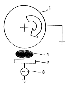
Figure 1 is a schematic view showing the construction
of a sputtering appratus including a rotating holder, as
used in Examples in accordance with the present invention;
Figure- 2 is a perspective view showing a rechargeable
lithium battery constructed in Examples in accordance with
the present invention;
Figure 3 is a schematic sectional view showing a
rechargeable lithium battery constructed in Examples in
accordance with the present invention;
Figure 4 is a graph showing a concentration distibution
of a copper element along a depth of the electrode of
Example 1;
Figure 5 is a graph showing a concentration distibution
of a copper element along a depth of the electrode of
Example 2;
Figure 6 is a graph showing a concentration distibution
of a copper element along a depth of the electrode of
Example 3;
-12-
CA 02388016 2006-07-27
i j
Figure 7 is a graph showing a concentration distibution
of a copper element along a depth of the electrode of
Comparative Example 1; and
Figure 8 is a graph showing a concentration distibution
of a copper element along a depth of the electrode of
Comparative Example 2.
BEST MODE FOR CARRYING OUT THE INVENTION
The present invention is below described in more detail
by way of examples. It should be understood that the
present invention is by no means limited by the folloiwng
examples, and suitable changes and modifications can be
effected without departing from the scope of the present
invention.
EXPERIMENT 1
Fabrication of Necsative Electrode:
A rolled copper foil (about 26 ~un thick) was roughend
at its surface via copper deposition by an electrolytic
process to provide a current collector. A silicon thin film
was formed on the current collector using a parallel-plate.
RF sputtering apparatus. An Ar gas alone was used as a
sputtering gas. 99.999 % pure, single crystal silicon was
used as a target. The negative electrodes of Examples 1 - 7
and Comparative Examples 1- 3 were fabricated under the
thin-film forming conditions as specified in Tables 1 and 2,
-13-
CA 02388016 2006-07-27
while adjusting a flow rate of the Ar gas or an opening
degree of an exhaust valve. The silicon thin film was
formed to a thickness of about 6pn.
In Examples 1 - 3 and Comparative Examples 1 - 2; the
substrate temperature was varied to form silicon thin films
(thin films of active material) at different thin-film
forming temperatures (maximum attainable temperatures). In
Example 4 and Comparative Example 3, the deposited thin
films were further subjected to a heat treatment under the
conditions specified in Table .2. In Examples 5 - 7, the
power density applied to the target was varied to form thin
films.
The crystallinities of the resulting silicon thin films
were identified by Ramanspectroscopy. The silicon thin
film was identified as being "amorphous" when the substantial
presence of a peak around 480 cm1 and the substantial
absence of a peak around 520 cnil were observed and as being
"polycrystalline" when the substantial absence of a peak
around 480 cml and the substantial presence of a single peak
around 520 cml were observed.
Each silicon thin film was deposited on a limited, 2.5
cm x 2.5 cm surface region of the copper foil by using a
mask. After deposition of the silicon thin film, a negative
electrode tab was attached onto a surface portion of the
copper foil that was left uncoated with the silicon thin
-14-
CA 02388016 2006-07-27
film to complete a negative electrode.
Fabrication of Positive Electrode:
90 parts by weight of LiCoO2 powder and 5 parts by
weight of artificial graphite powder as conductive material
were mixed in a 5 wt.% N-methylpyrrolidone aqueous solution
containing 5 parts by weight of polytetrafluoroethylene as a
binder to provide a mix slurry for positive electrode. This
slurry was coated by a doctor blade method onto a 2.5 cm x
2.5 cm surface region of an aluminum foil (about 18 ~un
thick) serving as a positive current collector and then
dried to provide a layer of positive active material. A
positive electrode tab was attached onto a surface region of
the aluminum foil that was left uncoated with the layer of
positive active material to complete a positive electrode.
Preparation of Electrolyte Solution:
1 mole/liter of LiPF6 was dissolved in a mixed solvent
containing equi-volumes of ethylene carbonate and dimethyl
carbonate to prepare an electrolyte solution for use in the
following battery construction.
Construction of Battery:
Figure 2 is a perspective view of such constructed
rechargeable lithium battery. Figure 3 is a schematic
sectional view of the constructed rechargeable lithium
battery. As shown in Figure 3, the positive electrode and
the negative electrode are inserted into an interior of a
-15-
CA 02388016 2006-07-27
casing 10. A layer of negative active material in the form
of a silicon thin film 12 is provided on a negative current
collector 11. A layer 14 of positive active material is
provided on a positive current collector 13. A separator 15
is interposed between the silicon thin film 12 and the layer
14 of positive active material. The electrolyte solution is
introduced into the casing 10. The casing 10 is welded at
its ends to define a sealed portion 10a. The negative
electrode tab 17 attached to the negative current collector
11 extends thourgh the sealed portion l0a to an outside.
Although not shown in Figure 3, the positive electrode tab
18 attached to the positive current collector 13 also
extends thourgh the sealed portion l0a to an outside.
Charge-Discharge Cycle Test:
The rechargeable lithium batteries constructed in_the
manner as described above were subjected to a charge-
discharge cycle test. Each battery was charged at a current
of 9 mA to a charge end capacity of 9 mAh and then
discharged at a current of 9 mA to a discharge end voltage
of 2.75 V. This unit charge-discharge cycle was repeated to
measure lst-cycle, 5th-cycle and 20th-cycle discharge
capacities and charge-discharge efficiencies. The results
are shown in Tables 1 and 2. In the following Tables, the
unit of flow rate, sccm, indicates' a volumetric flow rate
per minute (cm3/minute) of a fluid at 0 C at 1 atmospheric
-16-
CA 02388016 2002-04-18
pressure (101.33 kPa) and is an abbreviation of standard
cubic centimeters per minute.
Table 1
Ex.l Ex.2 Ex.3 Comp. Comp.
Ex.l Ex.2
Ar Flow Rate 50sccm 50sccm 50sccm 50sccm 50sccm
Sputtering 0.1Pa 0.1Pa 0.1Pa 0.1Pa 0.1Pa
Atmosphere
Thin Sputtering Power 300W 300W 300W 300W 300W
Film (Power Density (3.70) (3.70) (3.70) (3.70) (3.70)
Forming W/cm}
Condi- Substrate Ambient
tions Temperature (Not 2000C 250 C 3000C 400 C
(Initial) Heated)
Maximum About About About About About
Attainable 2900C 290 C 290 C 320 C 400 C
Temperature
Heat Temperature,
Treat- Time Absent Absent Absent Absent Absent
ment
Crystallininity Amor- Amor- Amor- Amor- Amor-
phous phous phous phous phous
Discharge 2144 2085 2546 524 707
lst Capacity(mAh/g)
Cycle Charge-Discharge 78 75 97 49 59
Efficiency($)
Discharge 2042 1963 2538 152 334
5th Capacity(mAh/g)
Cycle Charge-Discharge 100 100 99 78 86
Efficiency(g)
Discharge 1924 1827 2456
20th Capacity(mAh/g)
Cycle Charge-Discharge 99 99 99
Efficiency(%)
-17-
CA 02388016 2002-04-18
Table 2
Ex.4 ECom x.p3 Ex.5 Ex.6 Ex.7
Ar Flow Rate 50sccm 50sccm 100sccm 1o0sccmioosccm
S uttering 0.1Pa 0.1Pa 0.1Pa 0.1Pa 0.1Pa
A~mosphere
Thin Sputtering Power 300W 300W 50W 100W 400W
Film (Power Density (3.70) (3.70) (0.62) (1.23) (4.94)
Forming W/cm)
Condi- Substrate Ambient Ambient ~ztbient ~mbient ~mbient
tions Temperature (Not (Not (Not (Not (Not
( Initial ) eated) Heated) eated) eated) eated)
Maximum About Abo t About About About
Attainable 290 C 290 70 C 150 C 270 C
Temperature
Heat Temperature, 400 C, 650 C
Treat- Time lh lh ~Absent Absent Absent
ment
rystallinity Amor- pstal- ~or- Amor- Amor-
phous ~ine phous phous phous
Discharge 2016 1976 2.145 2419 2505
lst Capacity(mAh/g)
Cycle Charge-Discharge 91 81 88 91 92
Efficiency(~}
Discharge
5th Capacity (mAh/g) 1913 729 1827 2296 2399
Cycle Charge-Discharge 99 73 96 99 99
Efficiency ($)
Discharge
20th Capacity(mAh/g) 1816 348 1510 2182 2323
Cycle Charge-Discharge 99 57 99 99 99
Efficiency(%)
As clear from the results given in Table 1 for Examples
1 3 and Comparative Examples 1 - 2, high discharge
capacities and satisfactory charge-discharge efficiencies
are obtained when the thin-film forming temperature (maximum
attainable temperature) is below 300 C.
-18-
CA 02388016 2002-04-18
As clear from the results given in Table 1 for Example
1 and the results given in Table 2 for Example 4 and
Comparative Example 3, the silicon thin film is rendered
into a polycrystalline form and the discharge capacity and
charge-discharge efficiency drop when the deposition of the
thin film was followed by heat treatment at a temperature of
650 C. This demonstrates that a temperature for the heat
treatment is preferably below 650 C, more preferably 400 C
or lower.
As clear from the results given in Table 1 for Example
1 and the results given in Table 2 for Example 5 - 7, high
discharge capacities and satisfactory charge-discharge
efficiencies are obtained when the power.density applied to
a target during thin-film formation is 4.94 W/cm2 or lower.
The negative electrodes fabricated in Examples 1 - 3
and Comparative Examples 1 - 2 by varying the substrate
temperature so as to vary the thin-film forming temperature
(maximum attainable temperature) were measured for a
concentration distribution of a copper element in a depth
direction by SIMS (secondary ion mass spectrometry). Each
negative electrode before subjected to a charge-discharge
test was measured for a concentration distribution of a
copper element (63Cu+) using 02+ as a sputtering source.
Figures 4 - 8 illustrate concentration distributions of
copper along depths of the negative electrodes fabricated in
-19-
CA 02388016 2002-04-18
Examples 1 -3 and Comparative Examples 1 - 2. Each abscissa
indicates a depth (pm) and each ordinate indicates an atomic
density (atoms/cc : atoms/cm3). Figure 4 corrsponds to
Example 1, Figure 5 to Example 2, Figure 6 to Example 3,
Figure 7 to Comparative Example 1, and Figure 8 to
Comparative Example 2.
In any of Figures 4 - 8, the thin film has a thickness
region, in the vicinity of its top surface, where the copper
concentration shows no substantial change and is relatively
low. The thin film also has a thickness region where the
copper concentration increases from the top surface of the
thin film toward an interface between the thin film and the
current collector. The presence of such a thickness region
with an increaseing copper concentration clearly indicates
the existence of a mixed layer consisting of the active
material and the copper element in the thin film adjacent
the interface between the thin film and the current
collector. The existence of such a mixed region (mixed
layer) is believed to result in a marked improvement in
adhesion between the current collector and the thin film.
In Examples 1 - 3 (Figures 4 - 6) where thin films of
active material were deposited under the relatively low,
substrate temperature conditions, the copper concentration
near the top surface of each thin film is 1020 atoms/cc
(atoms/cm3) (about 1%). On the other hand, in Comparative
-20-
CA 02388016 2006-07-27
Examples 1 - 2 (Figures 7 - 8) where thin films of active
material were deposited under the relatively high, substrate
temperature conditions, the copper concentration near the
top surface of each thin film is 1021 atoms/cc (atoms/cm')
(about 10 %) or more. It is believed from these results
that if the thin film of active material is formed at higher
substrate temperatures, copper is diffused into an entire
region of the thin film and a concentration of the active
material relatively decreases to result in the reduced
discharge capacity. It is also believed that existence of
copper at a higher concentration in the thin film causes the
poorer cycle characteristics. This is probably due to the
production of an intermetallic compound in the thin film.
EXPERIMENT 2
Fabrication of Negative Electrode:
An RF sputtering apparatus with a rotating holder, as
shown in Figure 1, was utilized to form a silicon thin film.
The silicon thin film was deposited onto a current collector
similar in type to that used in Experiment 1. The current
collector was placed on an outer periphery of the rotating
holder 1 shown in Figure 1. While the rotating holder 1 was
rotated, a radio-frequency (RF) power from an RF power
supply 3 was supplied to the target 2 to generate an Ar
plasma 4, so that the silicon thin film was deposited on the
current collector. The rotating holder 1 was rotated at a
-21-
CA 02388016 2006-07-27
speed of about 10 rpm. Other thin-film forming conditions
are specified in Table 3. An Ar gas alone was used for the
sputtering gas. The target used was similar in type to that
specified in Experiment 1. The silicon thin film was
deposited to a thickness of about 6 ~un.
Construction of Battery and Charge-Discharge Cycle
Using a positive electrode similar in type to that
fabricated in Experiment 1, a rechargeable lithium batt-ery
was constructed in the same manner as in Experiment 1. The
battery was subsequently subjected to the charge-dis-charge
cycle test specified in Experiment 1. The results are shown
in Table 3.
Table 3
Ex.8-
Ar Flow Rate 50sccm
Sputtering Atmosphere 0.1Pa
Thin Film Sputtering Power Z 350W
Forming (Power Density W/cm) (4.32)
Conditions Substrate Temperature (Initial) Ambient
(Not Heated)
Speed of Holder Rotation 10 rpm
Maximum Attainable Temperature About 210
Heat Temperature, Time Absent
Treatment
Crystallinity Amorphous
1st Cycle Discharge apaci y g
Charge-DischargeEfficiency(%) 95
5th Cycle Discharge Capacity(mAh/g) 3172
Charge-Discharge Efficiency(%) 100
20th Cycle Discharge Capacity(mAh/g) 3016
Charge-Discharge Efficiency(%) 100
-22-
CA 02388016 2006-07-27
As apparent from the results shown in Table 3, the
deposition temperature (maximum attainable temperature) in
Example 8 is lower than in Example 1, although the power
density applied to the target in Example 8 is slightly
higher than in Example 1 and the remaining forming
conditions are identical. In Example 8, the current
collector is placed on a rotating holder and the active
material is deposited. thereon while the rotating holder is
rotated so that the deposition of silicon on the current
collector is achieved in an intermittent manner. This is
believed to successfully'hold the maximum attainable
temperature down at a lower level. It is also appreciated
that slightly better discharge capacity and charge-discharge
efficiency are obtained in Example 8 than in Example 1.
EXPERIMENT 3
The same parallel-plate sputtering apparatus as in
Experiment 1 was used. The procedure of Example 1 of
Experiment 1 was followed, except that a DC or pulse power,
instead of the radio-frequency (RF) power, was applied to
the target at the power density specified in Table 4, to
deposit a silicon thin film on a current collector and
fabricate a negative electrode.
Construction of Battery and Charge-Discharge Cycle:
Te2t;
Using a positive electrode similar in type to that
-23-
CA 02388016 2002-04-18
fabricated in Experiment 1, a rechargeable lithium battery
was constructed in the same manner as in Experiment 1. The
battery was subsequently subjected to the charge-discharge
cycle test specified in Experiment 1. The results are shown
in Table 4.
TABLE 4
Ex.9 Ex.10
Ar Flow Rate 85sccm 85sccm
Sputtering Atmosphere 0.4Pa 0.4Pa
Power Source DC Pulse
(100kHz)
Thin Film Sputtering Power 210W 420W
Conditions (Power Density W/cm2) (2.58) (5.17)
Substrate Temp erature Ambient Ambient
(Initial Heated) Heated)
Maximum Attainable Temperatur Abouot Abouot
200 C 100 C
Heat Temperature, Time Absent Absent
Treatment
Crystallinity Amorphous Amorphous
Discharge Capacity(mAh/g) 2340 2706
lst Cycle
Charge-Discharge Efficiency(%) 97 96
Discharge Capacity(mAh/g) 2349 2743
5th Cycle Charge-Discharge Efficiency(%) 100 100
Discharge Capacity(mAh/g) 2361 2739
20th Cycle
Charge-Discharge Efficiency(%) 99 99
As can be clearly seen from the results shown in Table
4, the use of a DC or pulse power source results in the
deposition temperature (maximum attainable temperature) that
is lower than that in Example 1. Also, the rechargeable
-24-
CA 02388016 2002-04-18
lithium batteries give satisfactory discharge capacity and
charge-discharge efficiency results which are almost
comparable to those of Example 1..
Although the.thin films of active material are formed
by a sputtering technique in the preceding Examples, the
present invention is not limited thereto. The CVD or other
thin-film forming processes can also be used.
UTILITY IN INDUSTRY
In accordance with the present invention, an electrode
for a rechargeable lithium battery can be stably fabricated
which exhibits a high charge-discharge capacity and superior
charge-discharge cycle characteristics.
-25-