Note: Descriptions are shown in the official language in which they were submitted.
, ;63 ,ll a ~,..
CA 02388213 2002-05-30
BALLAST WITH EFFICIENT FILAMENT PREHEATING
AND LAMP FAULT PROTECTION
00-1-217
Field of the Invention
The present invention relates to the general subject of circuits for
powering discharge lamps. More particularly, the present invention relates to
ballast that efficiently preheats the lamp filaments and that inherently
provides
lamp fault protection.
Background of the Invention
Electronic ballasts for gas discharge lamps are often classified into two
groups according to how the lamps are ignited - preheat and instant start. In
preheat ballasts, the lamp filaments are preheated at a relatively high level
(e.g.,
7 volts peak) for a limited period of time (e.g., one second or less) before a
moderately high voltage (e.g., 500 volts peak) is applied across the lamp in
order to ignite the lamp. In instant start ballasts, the lamp filaments are
not
preheated, so a higher starting voltage (e.g., 1000 volts peak) is required in
order
to ignite the lamp. It is generally acknowledged that instant start operation
offers certain advantages, such as the ability to ignite the lamp at a lower
ambient temperatures and greater energy efficiency (i.e., light output per
watt)
due to no expenditure of power on filament heating during normal operation of
the lamp. On the other hand, instant start operation usually results in
considerably lower lamp life than preheat operation.
Because a substantial amount of power is unnecessarily expended on
heating the lamp filaments during normal operation of the lamp, it is
desirable to
have preheat ballasts in which filament power is minimized or eliminated once
the lamp has ignited. Currently, there are at least three main approaches for
achieving this goal. A first approach, which may be called the "passive"
method, heats the filaments via windings on a transformer that also provides
the
high voltage for igniting the lamp. An acknowledged drawback of this approach
is a limit on the degree to which filament heating power may be reduced once
the lamp ignites and begins to operate; a detailed discussion of the
difficulties
CA 02388213 2012-08-16
2
with this approach is provided in the "Background of the Invention" section of
U.S. Patent
5,998,930.
A second approach, which is common in so-called "programmed start" products,
employs an inverter that is operated at one frequency in order to preheat the
lamp
filaments, then "swept" to another frequency in order to ignite and operate
the lamp.
Because this approach is difficult and/or costly to implement in ballasts
having self-
oscillating type inverters, it is usually employed only in ballasts having
driven type
inverters. This approach has the further disadvantage of producing a
significant amount of
"glow current" through the lamp immediately prior to ignition. Glow current is
generally
considered to negatively impact the useful life of the lamp.
A third approach employs switching circuitry that disconnects the source of
filament power from each of the filaments after the lamp ignites. This
approach tends to
be rather costly to implement, especially in ballasts that power multiple
lamps because
multiple switching circuits are required (i.e., one for each filament or each
pair of parallel-
connected filaments).
All of the aforementioned approaches are largely limited in function to
filament
heating and do not provide any separate benefits, such as automatic relamping
capability or
prevention of the high voltages, currents, and power dissipation that
generally occurs
following lamp removal or failure. Because ballasts that implement these
approaches
generally require separate, dedicated circuitry in order to accommodate
relamping and
protect the ballast from damage due to lamp removal or failure, the resulting
ballasts tend
to be functionally and structurally complex.
What is needed, therefore, is a ballast in which: (i) the filaments are
properly
preheated prior to lamp ignition; (ii) little or no power is expended on
filament heating
during normal operation of the lamp; and (iii) little or no pre-ignition glow
current occurs.
A need also exists for a filament heating reduction approach that is readily
implemented in
ballasts having either driven or self-oscillating inverters. A further need
exists for a
filament heating reduction approach that accommodates relamping and that
provides lamp
fault protection without requiring extensive additional circuitry. A ballast
with these
attributes would represent a significant advance over the prior art.
Summary of the Invention
According to an aspect of the present invention there is provided a ballast
for
powering at least one gas discharge lamp having heatable filaments,
comprising: an
inverter having a pair of inputs and an output; and operable to receive a
substantially direct
CA 02388213 2012-08-16
3
current (DC) voltage and to provide an alternating voltage at the inverter
output; first,
second, third, and fourth output connections adapted for connection to the
lamp, wherein
the first and second output connections are coupled to a first filament of the
lamp, and the
third and fourth output connections are coupled to a second filament of the
lamp; a
resonant inductor coupled between the inverter output and the first output
connection; a
resonant capacitor coupled between the first output connection and a first
node; a direct
current (DC) blocking capacitor coupled between the fourth output connection
and circuit
ground; a filament heating and protection circuit coupled to the first node
and the first,
second, third, and fourth output connections and circuit ground, and operable
to provide:
(i) a filament preheating mode wherein a voltage across each filament is
maintained at a
preheat level, and a voltage between the first and fourth output connections
is maintained
at a pre-ignition level, in order to preheat the filaments prior to attempting
to ignite the
lamp; (ii) an ignition mode wherein the voltage between the first and fourth
output
connections is increased to an ignition level that is greater than the pre-
ignition level; (iii) a
normal operating mode wherein the voltage across each filament is maintained
at an
operating level that is substantially less than the preheat level; and (iv) a
fault mode
wherein the filament preheating mode and the ignition mode are repeated in
response to a
lamp fault condition, wherein the filament heating protection circuit
comprises: a
transformer, comprising: a primary winding coupled between the first node and
circuit
ground; a first auxiliary winding coupled to the first and second output
connections; and a
second auxiliary winding coupled to the third and fourth output connections; a
switching
circuit coupled between the first node and circuit ground and operable to turn
on and
provide a low impedance AC path between the first node and circuit ground
during the
ignition mode and during the normal operating mode; a turn-on circuit coupled
to the
switching circuit and operable to turn the switching circuit on during the
ignition mode
following completion of the filament preheating mode; and a lamp-out detection
circuit
coupled to the fourth output connection and the switching circuit and operable
to keep the
switching circuit on during the normal operating mode, and to turn the
switching circuit off
in response to the lamp fault condition.
Brief Description of the Drawings
Fig. 1 is a partial block-diagram schematic of a ballast that includes a
filament
heating and protection circuit, in accordance with the present invention.
CA 02388213 2012-08-16
3a
Fig. 2 describes a preferred arrangement for the filament heating and
protection
circuit referred to in FIG. 1, in accordance with a preferred embodiment of
the present
invention.
Fig. 3 describes a preferred arrangement for the control circuit referred to
in FIG. 2,
in accordance with a preferred embodiment of the present invention.
FIG. 4 describes preferred arrangements for the switching circuit, turn-on
circuit,
and lamp-out detection circuit referred to in FIG. 3, in accordance with a
preferred
embodiment of the present invention.
FIG. 5 includes several approximate waveforms that describe the detailed
operation
of the filament heating and protection circuit, in accordance with a preferred
embodiment
of the present invention.
CA 02388213 2002-05-30
4
Detailed Description of the Preferred Embodiments
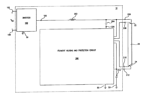
FIG. 1 describes a ballast 10 for powering at least one gas discharge
lamp 20 having heatable filaments 22,24. Ballast 10 includes an inverter 100,
output connections 206,208,210,212, a resonant inductor 202, a resonant
capacitor 204, a direct current (DC) blocking capacitor 214, and a filament
heating and protection circuit 300.
Inverter 100 has a pair of inputs 102,104 and an output 106. During
operation, inverter 100 receives a substantially direct current (DC) voltage,
VDC,
and provides an alternating voltage at inverter output 106. Preferably, VDC is
a
substantially direct current (DC) voltage that may be provided, for example,
via
a rectifier and boost converter arrangement that receives conventional AC
voltage (e.g., 120 Vrms at 60 Hz) and provides a desired DC voltage (e.g., 350
volts). The alternating voltage at inverter output 106 has a high frequency
(e.g.,
20,000 hertz or greater) that is at or near to the natural resonant frequency
of
inductor 202 and capacitor 204. Output connections 206,208,210,212 are
adapted for connection lamp 20, wherein first and second output connections
206,208 are coupled to a first filament 22 of lamp 20, and third and fourth
output connections 210,212 are coupled to a second filament 24 of lamp 20.
Resonant inductor 202 is coupled between inverter output 106 and first output
connection 206. Resonant capacitor 204 is coupled between first output
connection 206 and a first node 220. DC blocking capacitor 214 is coupled
between fourth output connection 212 and circuit ground 50.
Filament heating and protection circuit 300 is coupled to first node 220
and output connections 206,208,210,212. Filament heating and protection
circuit 300 provides a number of different modes of operation, including a
filament preheating mode, an ignition mode, a normal operating mode, and a
fault mode. During the filament preheating mode, the voltage (VFR,) across
each
filament 22,24 is maintained at a preheat level (e.g., 7 volts peak) and the
voltage (Amp) applied to the lamp (e.g., the voltage between the first and
fourth output connections 206, 212) is maintained at a pre-ignition level
(e.g.,
175 volts peak) in order to preheat the filaments prior to attempting to
ignite the
G: :II
CA 02388213 2002-05-30
lamp. During the ignition mode, Vjp is increased to an ignition level (e.g.,
1000 volts peak) that is greater than the pre-ignition level (e.g., 175 volts
peak)
in order to ignite the lamp. During the normal operating mode, VFa, is
maintained at an operating level (e.g., 0.5 volts peak) that is substantially
less
5 than the preheat level (e.g., 7 volts peak) in order to conserve power
expended
on heating the filaments. During the fault mode, the filament preheating mode
and the ignition mode are repeated in response to a lamp fault condition.
Preferably, a lamp fault condition is deemed to have occurred when the lamp is
disconnected and/or when the lamp fails to conduct current following
completion of the ignition mode.
Turning now to FIG. 2, filament heating and protection circuit 300
preferably includes a transformer 400 and a control circuit 500.
Transformer 400 includes a primary winding 402, a first auxiliary
winding 404, and a second auxiliary winding 406. Primary winding 402 is
coupled between first node 220 and circuit ground 50. First auxiliary winding
404 is coupled to first and second output connections 206,208. Second
auxiliary
winding 406 is coupled to third and fourth output connections 210,212.
Control circuit 500 is coupled to first node 220, fourth output connection
212, and circuit ground 50. During operation, control circuit 500 selectively
provides a low impedance alternating current (AC) path between first node 220
and circuit ground 50. More specifically, the low impedance AC path is
provided during the ignition and normal operating modes, but not during the
filament preheating mode. The low impedance AC path provided by control
circuit 500 has an impedance that, for the high frequency current that flows
through resonant inductor 202 and resonant capacitor 204, is substantially
less
than the impedance of primary winding 402. Thus, control circuit 500
effectively shunts the current that normally flows through primary winding 402
to circuit ground 50 during the ignition and normal operating modes, so that a
high voltage is developed for igniting the lamp (by virtue of resonant
capacitor
204 having a low impedance path to circuit ground 50) and filament power is
substantially eliminated during normal operation of the lamp.
CA 02388213 2002-05-30
6
As described in FIG. 3, in a preferred embodiment, control circuit 500
includes a switching circuit 600, a turn-on circuit 700, and a lamp-out
detection
circuit 800. Switching circuit 600 is coupled between first node 220 and
circuit
ground 50. Switching circuit 600 is functional to selectively turn on and
provide a low impedance AC path between first node 220 and circuit ground 50.
Turn-on circuit 700 is coupled to switching circuit 600, and is operable to
turn
switching circuit 600 on during the ignition mode following completion of the
preheating mode. Lamp-out detection circuit 800 is coupled to switching
circuit
600 and fourth output connection 212. Lamp-out detection circuit 800 keeps
switching circuit 600 on during the normal operating mode, and turns switching
circuit 600 off in the event of a lamp fault condition.
Switching circuit 600, turn-on circuit 700, and lamp-out detection circuit
800 are preferably realized as described in FIG. 4. Switching circuit 600
includes a switch 610 having a control terminal 612, a first conduction
terminal
614, and a second conduction terminal 616. First conduction terminal 614 is
indirectly coupled to first node 220, and second conduction terminal 616 is
coupled to circuit ground 50. As described in FIG. 4, switch 610 is preferably
implemented as a field-effect transistor (FET) having a drain terminal
(corresponding to first conduction terminal 614), a source terminal
(corresponding to second conduction terminal 616), and a gate terminal
(corresponding to control terminal 612). Switching circuit further includes a
capacitor 620 having a first end 622 coupled to first node 220 and a second
end
624 coupled to drain terminal 614 of FET 610. Capacitor 620 serves two
functions that are relevant when switch 610 is implemented using a FET. First,
during periods when switch 610 is on, capacitor 620 functions as a low
impedance AC coupling capacitor for coupling first node 220 to circuit ground.
Second, during periods when switch 610 is off (i.e., during filament
preheating),
capacitor 620 functions as a DC blocking capacitor which ensures symmetry
(i.e., no significant DC component) in the voltage across primary winding 402.
Switching circuit 600 and transformer 400 provide two main functional
benefits. First, they function as a filament "cut-out" circuit that preheats
the
lamp filaments at a relatively high level for a limited period of time, and
then
CA 02388213 2002-05-30
7
dramatically reduces the filament power in order to operate the lamp in an
energy-efficient manner. Second, switching circuit 600 and transformer 400
serve as part of a lamp fault protection circuit that prevents sustained high
voltages and currents, and minimizes power dissipation, following removal or
failure of the lamp.
Switching circuit preferably further includes a clamp diode 630 having
an anode 632 coupled to drain terminal 614 of FET 610, and a cathode 634
coupled to a first input 102 of inverter 100. Clamp diode 630 prevents the
voltage at drain terminal 614 from exceeding the inverter input voltage, VDC
(e.g., 350 volts), thereby allowing FET 610 to be realized by a device with a
reasonable drain-to-source voltage rating (e.g., 400 volts). In the absence of
clamp diode 630, the voltage rating of FET 610 would have to be considerably
greater and, consequently, FET 610 would be more costly.
Lamp-out detection circuit 800 preferably includes a first capacitor 802,
a first diode 810, a second diode 820, a second capacitor 830, and a resistor
832.
First capacitor 802 is coupled between fourth output connection 212 and a
second node 804. First diode 810 has an anode coupled to circuit ground 50 and
a cathode 814 coupled to second node 804. Second diode 820 has an anode 822
coupled to second node 804 and a cathode 824 coupled to gate terminal 612 of
FET 610. Second capacitor 830 and resistor 832 are each coupled between gate
terminal 612 of FET 610 and circuit ground 50. With an appropriate choice of
component values, lamp-out detection circuit 800 is capable of turning
switching circuit 600 off within less than one millisecond after occurrence of
a
lamp fault condition. This response time is significantly faster than prior
art
approaches, and is attributable to the fact that lamp-out detection circuit
800 is
capacitively coupled to output connection 212, which allows lamp-out detection
circuit 800 to monitor lamp current rather than the DC voltage across DC
blocking capacitor 214. In order to ensure a fast response, it is preferred
that the
capacitance of capacitor 802 be at least an order of magnitude smaller than
that
of DC blocking capacitor 214.
The operation and advantages of lamp-out detection circuit 800 is
described in greater detail in the present inventor's copending U.S. patent
CA 02388213 2002-05-30
8
application entitled "Ballast with Fast-Responding Lamp-Out Detection Circuit"
(filed on the same day and assigned to the same assignee as the present
application).
Turn-on circuit 700 preferably includes a first resistor 702, a capacitor
706, a voltage-triggered device 708, a second resistor 710, and a diode 720.
First resistor 702 is coupled between inverter output 106 and a third node
704.
Capacitor 706 is coupled between third node 704 and circuit ground 50.
Voltage-triggered device 708, preferably implemented as a diac, is coupled
between third node 704 and gate terminal 612 of FET 610. Second resistor 710
is interposed between diac 708 and gate terminal 612 of FET 610. Diode 720
has an anode 722 coupled to third node 704 and a cathode 724 coupled to gate
terminal 612 of FET 610.
When inverter 100 begins to operate after power is applied to ballast 10,
a substantially squarewave voltage that varies between zero and VDC is present
at inverter output 106. Capacitor 706 begins to charge up via resistor 702.
Approximately one second after inverter 100 begins to operate, the voltage
across capacitor 706 reaches a predetermined trigger voltage (i.e., the
"breakover" voltage of diac 708; e.g., 32 volts) and diac 708 turns on and
couples third node 704 to gate terminal 612 of FET 610 via resistor 710.
Consequently, FET 610 turns on. Once FET 610 turns on, third node 704 is
coupled to circuit ground via diode 720, so the voltage at third node 704
drops
to near zero. Diac 708 turns off and remains off for at least as long as FET
610
remains on. If FET 610 is subsequently turned off, the preceding turn-on cycle
will repeat itself, and FET 610 will be turned on again after about one
second.
Turn-on circuit 700 may be implemented using any other type of circuit
that periodically provides a pulse of limited duration for turning on switch
610
for a limited period of time. For example, although not shown or described in
detail herein, turn-on circuit 700 may be implemented using an appropriate
timer circuit that delays providing a pulse for a fixed period of time after
inverter 100 begins to operate (i.e., so that proper filament preheating is
provided) and after occurrence of a fault condition (i.e., so that automatic
relamping capability is provided).
1"'a~I l
CA 02388213 2002-05-30
9
As a consequence of using the diac-based turn-on circuit 700 shown in
FIG. 4, it is preferred that switching circuit 600 further include a first
diode 640
and a second diode 650. First diode 640 has an anode 642 coupled to the second
end 624 of capacitor 620 and a cathode 644 coupled to the drain terminal 614
of
FET 610. Second diode 650 has an anode 652 coupled to circuit ground 50 and
a cathode 654 coupled to the second end 624 of capacitor 620. The function of
second diode 650 is, when FET 610 is on, to provide a circuit path for the
negative half-cycles of the high frequency current that flows through resonant
capacitor 204. Note that second diode 650 is only required because of the
presence of first diode 640 (which, in turn, is only required because of diode
720
in turn-on circuit 700). If a different type of turn-on circuit is used, diode
640
may not be required and second end 624 of capacitor 620 may be connected
directly to the drain terminal 614 of FET 610, in which case the built-in
drain-
to-source diode (not shown) of FET 610 would serve the same function as diode
650.
A prototype ballast configured substantially as depicted in FIG. 4 was
built and tested. VDc was set to 350 volts, the inverter operating frequency
was
set at approximately 48 kilohertz, and the following component values and part
numbers were used:
Inductor 202: 2.8 millihenries
Capacitor 204: 3.9 nanofarads, 1.4 kilovolt
Capacitor 214: 0.1 microfarads, 400 volts
Transformer 400:
Primary winding 402: 150 turns (inductance = 25 millihenries)
Auxiliary windings 404,406: 5 turns each
Switching circuit 600:
FET 610: 4N60
Capacitor 620: 0.1 microfarads, 400 volts
Diode 630: RGP l OJ
Diode 640: RGP 10J
Diode 650: RGP10J
Zener diode 660: 1N4740A (zener voltage = 10 volts)
CA 02388213 2002-05-30
Turn-on circuit 700:
Resistor 702: 440 kilohms (two - 220 kilohm, 1/4 watt resistors in series)
Capacitor 706: 1 microfarad, 50 volts
5 Diac 708: breakover voltage = 32 volts
Resistor 710: 30 ohms,'/4 watt
Diode 720: 1N4007
Lamp-out detection circuit 800:
10 Capacitor 802: 0.0047 microfarads, 400 volts
Diode 810: 1N4148
Diode 820: 1N4148
Capacitor 830: 0.047 microfarad, 50 volts
Resistor 832: 20 kilohms, 1/4 watt
The detailed operation of ballast 10 is now explained with reference to
FIGs. 4 and 5 as follows. In FIG. 5, VFIL represents the voltage across each
filament 22,24 of lamp 20; that is, VFIL represents both the voltage between
output connection 206 and output connection 208, and the voltage between
output connection 210 and output connection 212. VLAmp is the voltage that is
applied between opposing ends of lamp 20; for example, VLAMIP may be thought
of as the voltage between output connection 206 and output connection 212.
ILAMp is the actual current that flows in the arc of the lamp when the lamp is
ignited. VGS is the gate-to-source voltage (i.e., the voltage between gate
terminal 612 and source terminal 616) of FET 610. For purposes of clarity and
ease of explanation, the waveforms in FIG. 5 are, in at least some instances,
simplified approximations of the waveforms that would actually be observed on
an oscilloscope during operation of ballast 10. For example, each of VFIL,
VLF, and ILAmp are depicted in terms of the peak values of the actual signal;
in
reality, each of these signals is an alternating current (AC) signal that
symmetrically varies between negative and positive values. Additionally, FIG.
5
depicts several abrupt transitions in value that would not necessarily occur
in so
orderly a manner in the actual ballast, where a certain degree of transient
behavior is typical. Finally, the time-scale of the waveforms in FIG. 5 is
compressed in a number of instances (i.e., as denoted by "= = ... ) in order
to better
CA 02388213 2002-05-30
11
illustrate what occurs within each ignition cycle (i.e., t2 to t3, t4 to t5,
t6 to t7, and
so forth).
At time to, power is applied to the ballast. Because the inverter has not
yet started to operate, VFIL, VIP, Iip, and VGS are all initially at zero.
At time t1, which typically occurs within less than 0.5 seconds after time
to, inverter 100 begins to operate and provide a substantially squarewave
output
voltage having a frequency at or near the natural resonant frequency (e.g., 48
kilohertz) of resonant inductor 202 and resonant capacitor 204. Within turn-on
circuit 700, capacitor 706 begins to charge up though resistor 702. Because
FET 610 is still off at this point, almost all of the current flowing through
resonant capacitor 204 also flows through primary winding 402; although diode
650 and capacitor 620 initially provide a path for negative-going current,
that
path quickly becomes insignificant once capacitor 620 peak charges to V0c/2 in
the negative direction (i.e., + sign at 624, - sign at 622). The inductance
of.
primary winding 402 is significant enough relative to that of resonant
inductor
202 to prevent inductor 202 and capacitor 204 from developing the high
voltages that otherwise appear across each when first node 220 is AC coupled
to
circuit ground 50.
During the period between tt and t2, VFIL is at a relatively high level (e.g,
7 volts). In contrast, VLip is at a relatively low level (e.g, 175 volts) that
is not
only insufficient to ignite the lamp, but that is also low enough so that
little
glow current flows through the lamp. Imp is still at zero because the lamp has
not yet ignited. Finally, VGS is at zero because diac 708 in turn-on circuit
700
has not yet turned on.
At time t2, the voltage across capacitor 706 reaches the breakover
voltage (e.g., 32 volts) of diac 704. Consequently, diac 720 turns on and
current
flows out of capacitor 706 and into resistor 832 and capacitor 830 via
resistor
710. Because of this current, the voltage at gate terminal 612 rapidly reaches
a
value that exceeds the minimum turn-on voltage (e.g., 4 volts) of FET 610, so
FET 610 turns on. Zener diode 660 limits the voltage at gate terminal 612 to a
safe value (e.g., 10 volts) in order to prevent damage to FET 610. With FET
610 now on, diode 720 becomes forward-biased and capacitor 706 rapidly
Fr I I
CA 02388213 2002-05-30
12
discharges to circuit ground via FET 610. Diac 708 thus turns off because the
voltage across capacitor 706 has fallen below the sustaining voltage (e.g., 28
volts) of the diac. With FET 610 on, node 220 is AC coupled to circuit ground
50 via capacitor 620, diode 640, and FET 610. Because capacitor 620 has a
capacitance that is at least an order of magnitude larger than that of
resonant
capacitor 204, and an impedance that is substantially smaller than the
impedance
of primary winding 402, almost all of the high frequency current that flows
through resonant capacitor 204 bypasses primary winding 402 and flows to
ground via capacitor 620 and: (i) diode 640 and FET 610 (for the positive half
cycles); or (ii) diode 650 (for the negative half cycles). As a result, the
voltage
across primary winding 402 is greatly reduced and, correspondingly, VFIL is
greatly reduced (e.g., from 7 volts down to 1 volt or less). At the same time,
VLwp increases dramatically (e.g., from 175 volts to 1000 volts) because the
effective AC short across primary winding 402 allows resonant inductor 202
and resonant capacitor 204 to behave substantially as a conventional series
resonant circuit that is excited at or near its resonant frequency. In this
way,
ballast 10 initially provides a high filament voltage for preheating the lamp
filaments, then reduces the filament preheating voltage and provides a high
voltage for attempting to ignite the lamp.
Between t2 and t3, with diac 708 off and capacitor 706 discharged, FET
612 remains on because the voltage across capacitor 830 exceeds the minimum
turn-on voltage of the FET. Although FET 610 requires little current to remain
on, VGs nonetheless decreases because capacitor 830 discharges into resistor
832.
At time t3, lamp 20 ignites and thus begins to conduct current. VL"p
rapidly falls to about 200 volts (the typical peak voltage across an F32T8
lamp
operated at rated current) because the ignited lamp presents a substantial
load to
the resonant circuit. With lamp 20 now operating, a small amount of AC
current flows into lamp-out detection circuit 800 and through capacitor 802.
Diode 820 allows only positive-going current to pass through to capacitor 830.
Diode 810 allows negative-going current to flow up from circuit ground 50 and
back through capacitor 802, thereby preventing capacitor 802 from peak-
[.,, ilk I
CA 02388213 2002-05-30
13
charging so that it can continue to provide AC coupling. The component values
for capacitors 803,830 and resistor 832 are selected such that the
substantially
DC voltage across capacitor 830 will be an appropriate value (e.g., 8 volts)
for
safely keeping FET 610 turned on. The function of resistor 832 is to discharge
capacitor 830, and thus turn FET 610 off, within a limited period of time
(i.e.,
less than one millisecond) in the event of a lamp fault. The resistance of
resistor
832 should be large enough relative to the capacitance of capacitor 830 to
ensure that FET 610 will remain on for at least long enough a time to achieve
ignition of an operable lamp; once the lamp ignites, capacitor 830 will be
replenished by a small portion of the lamp current via capacitor 802 and diode
820. On the other hand, to ensure fast response to a lamp fault, resistor 832
should have a resistance that is small enough relative to the capacitance of
capacitor 830 in order to cause VGS to fall to less than the minimum turn-on
voltage (e.g., 4 volts) of the FET within less than one millisecond after
capacitor
830 ceases to be replenished via capacitor 802 and diode 820.
Between t3 and t4, lamp 20 operates normally and VGS remains at a level
(e.g, 8 volts) that keeps FET 610 on. During this time, VFU, remains at a low
level (e.g., 0.5 volts or less), so very little power is expended on heating
the
lamp filaments. In applications where the lamp is operated with a lower value
of IMP, it might be desirable to actually increase the operating value of VFIL
during this period in order to ensure proper filament temperature. Such an
increase can be accomplished, within limits, merely by selecting a smaller
capacitance for capacitor 620. However, the capacitance of capacitor 620
should not be decreased to the point of becoming comparable to (e.g., less
than
ten times) that of resonant capacitor 204, as that would likely affect the
resonant
circuit and possibly reduce the ignition voltage.
It is assumed that, at time t4, the lamp is either removed or the lamp
suddenly fails to conduct current. As a result of removal of the lamp load,
VIP increases to its ignition level. Because IMP is now zero, no current
flows into capacitor 802 in order to maintain the voltage across capacitor 830
at
its operating level of about 8 ,volts. Capacitor 830 discharges through
resistor
832 and VGS begins to decrease.
CA 02388213 2002-05-30
14
At time t5, VGS finally falls below the level (e.g., 4 volts) necessary to
keep FET 610 on, so FET 610 turns off. With FET 610 off, the approximate
AC short across primary winding 402 is removed and primary winding 402 is
again effectively in series with resonant capacitor 204. This causes Vp to
fall to a relatively low level (e.g., 175 volts), and VFIL to return to its
preheat
level (e.g., 7 volts) because the voltage across primary winding 402 is now
much greater than it was when FET 610 was on.
Beginning at time t5, once FET 610 is turned off, diode 720 becomes
reverse-biased and allows capacitor 706 to begin charging up through resistor
702. After time t5, VGS continues to decrease and asymptotically approaches
zero as capacitor 830 continues to discharge through resistor 832
At time t6, which is approximately one second after time t5, the voltage
across capacitor 706 reaches the breakover voltage (e.g., 32 volts) of diac
708.
Diac 708 turns on and causes FET 610 to turn on, in the same manner as
previously described. With FET 610 on, primary winding 402 is effectively
shunted, resonant inductor 202 and resonant capacitor 204 achieve resonant
operation, V11p increases to its ignition level, and VFIL decreases from its
preheat level to its operating level.
. Between t6 and t7, which is a period of less than one millisecond, VGS
continuously decreases from its initial value of 10 volts. Because the removed
or failed lamp has yet to be replaced with a "good" lamp, lamp ignition cannot
occur. Absent an operating lamp, no sustaining current is provided to lamp-out
detection circuit 800, and VGS thus continues to decrease.
At time t7, which occurs within one millisecond after time t6, VGS falls
below 4 volts and FET 610 turns off. Vp returns its lower level and VFa.
returns to its preheat level, where both remain until the next ignition cycle
commences about one second later at time t8.
Assuming that the lamp fault is not cured, the ignition cycle that occurs
between tg and t9 will proceed in exactly the same way as previously described
for the cycle between t6 and t7. The ballast will continue to provide periodic
ignition cycles until at least such time as the lamp fault is cured or ballast
power
is removed. Advantageously, because each ignition cycle has a duration of less
CA 02388213 2012-08-16
than one millisecond, and the time between successive ignition cycles is about
one second,
the average power dissipated in the ballast will be very low during a lamp
fault condition.
If the lamp is replaced at some time between t9 and t10, the replaced lamp
will be
successfully ignited during the ignition cycle that occurs between t10 and
t11, in the same
5 manner as previously described with regard to the ignition cycle that occurs
between t2 and
t3. In this way, ballast 10 provides for automatic ignition upon replacement
of a failed or
removed lamp.
Ballast 10 offers a number of significant advantages over prior approaches.
Ballast
10 employs a filament heating and protection circuit that requires only a
modest amount of
10 electrical circuitry, but that provides a number of functional benefits.
First, ballast 10 offers
a substantial savings in energy consumption by minimizing unnecessary heating
of lamp
filaments during normal operation of the lamp(s). Second, ballast 10 provides
an abrupt
ignition voltage at a high level that quickly produces full arc current, thus
enhancing the
useful life of the lamp while also providing superior "cold starting"
capability.
15 Additionally, ballast 10 includes inherent protection that prevents
excessive voltages,
currents, and power dissipation in the event of lamp removal or failure.
Ballast 10 also
accommodates relamping, as it provides for automatic ignition of a replaced
lamp. Further,
ballast 10 is easily modified (i.e., by reducing the capacitance of capacitor
620; see FIG. 4)
so as to provide at least some level of filament heating, if desired. The
result is a reliable,
cost-effective ballast that operates lamps in an energy-efficient and life-
preserving manner.
Although the present invention has been described with reference to certain
preferred embodiments, numerous modifications and variations can be made by
those
skilled in the art. For example, although the drawings refer to a ballast with
a single gas
discharge lamp, it should be understood that the present invention is equally
applicable to
ballasts that power multiple lamps. Moreover, although it is believed that use
of a FET in
the switching circuit constitutes a best mode of practicing the present
invention, the use of
other controllable switching devices, such as a bipolar junction transistor or
an
electromechanical relay, has also been contemplated.