Note: Descriptions are shown in the official language in which they were submitted.
CA 02388350 2002-04-16
REVISED PAGES
PCT/EP00/11618 OlTK 0487WOP
[2345/174]
OPTICAL SPECTROSCOPY DEVICE AND METHOD FOR ITS MANUFACTURE
The present invention is directed to a device for use in
optical spectroscopy and to a method for its manufacture.
Numerous optical spectroscopy devices are known which can be
used for various spectroscopic methods. In these devices
essentially made up of optical spectrometers, the optical
radiation to be analyzed can be excited by various physical
processes of the substances to be analyzed. Such excitation
processes can be of the thermal, electrical, and/or optical
type. The devices necessary for this, such as those of a light
source, can be contained both in the spectrometers themselves,
but also provided externally thereto.
Depending on the substances to be analyzed, specific
conditions must be able to be fulfilled, for instance with
respect to the spectral region to be analyzed or the
excitation energy to be applied.
Thus, for example, in the pharmaceutical industry, optical
spectroscopy is increasingly being used for chemical
reactions, to verify when new active substances are produced.
In this context, essentially fluorescence radiation is
analyzed.
Because of the multiplicity of possible reaction products
produced by chemically reacting new as well as known
substances with each other, efficient analysis devices and/or.
NY01 466733 v 1 REVISED PAGES
CA 02388350 2002-04-16
methods are sought. Moreover, due to this multiplicity, an
ever smaller quantity is selected to be available for an
analysis. Thus, it is already known to fill reaction vessels
positioned in a row-type or planar array, in the form of
saucers having a volumetric capacity of about 1x10⁻⁶ 1, with
reagents. In this context, the up to a few thousand saucers of
a test row are filled with the reagents using automated
micropipettes. The reagents are used, in part, in small
quantities, for instance in the range of 10-12 1.
These saucers are then observed using optical measuring
methods and measured with respect to a specific reaction
product. The existence of a reaction is ascertained in the
process by observing fluorescing molecules that were attached
to the reagents. One determines whether the reaction took
place by measuring the reaction rate of the molecules of the
reaction product. In this context, the measured displacement
can be ascertained, for instance, by subjecting the reaction
vessel to a defined luminous exposure. The time duration of
the emission of such a fluorescence radiation is measured, for
example, by taking a time measurement of the fluorescent light
obtained following spectrometric decomposition. From this,
inferences are made regarding the reaction that took place and
the reaction products obtained. The measurement is performed
in a computer-controlled operation and, in this context, the
measuring system is moved from reaction volume to reaction
volume, i.e., the array of reaction vessels is moved along
under a microscope.
As measuring systems, one uses macroscopic fluorescence
microscopes having illumination lasers, classic illumination
and in-line imaging optics, including beam splatters and
subsequent spectrometers. However, due to their massive
design, measuring systems of this kind, as described by G.
Gradi et al. in Bio Methods, vol. 10, pp. 331-351, Birkhauser
Publishers Basel and by S. Sterrer in J. of Receptor and
Signal Transduction Research, vol. 17, 1997, pp. 511-520,
NY01 466733 v t 2 REVISED PAGES
.,
CA 02388350 2002-04-16
limit the application to an only very limited reaction space.
From EP-A 2-0709659, one can infer a miniaturized, integrated
spectrometer, where the objective is to accommodate all
components, including the radiation source, of the detector
and the control electronics on one single substrate.
In addition, from LVO 99/53350, one can infer a monolithic
infrared spectrometer, which includes a waveguide produced
from silicon, which is designed to include the necessary
components for performing an analysis, such as the reflector
fmirrorl and a grating. However, it is not used for the
analysis of visible light, since silicon is non-transparent in
the visible re iq on.
The object of the present invention is, therefore, to provide
an optical spectroscopy device, in particular a fluorescence
spectrometer, whose dimensions will be adaptable to the
increasingly smaller reaction volumes to be analyzed, and
which, because of its design, will enable a higher throughput
rate to be attained during the analysis. It is a further
object of the present invention to provide a device which is
able to be produced simply, quickly and cost-effectively in
industrial manufacturing, and operated in reliable fashion.
The achievement of these objectives is embodied in the
features of Claims 1 and 15, respectively.
Due to its dimensional design, the device advantageously
renders possible a short-focal-length focusing and exposure
optics, thereby facilitating a high numerical aperture.
Moreover, the time constants of the detectors may be clearly
reduced, i.e., their upper critical frequencies increased,
accompanied simultaneously by a high sensitivity. In addition,
in the context of the device according to the present
invention, both the detector-induced dead times, as well as
experimental retrofitting of the spectrometers are reduced.
NYO~ ass733 v i 3 REVISED PAGES
CA 02388350 2002-04-16
Further advantageous features of the present invention are
derived from the dependent claims.
The optical spectroscopy device according to the present
invention includes at least one light source and at least one
spectrometer produced as an integrated spectrometer, the
optical components of the at least one spectrometer being
optical microcomponents which are applied integratively to the
top and/or bottom side of a substrate board. For the present
invention, it is unimportant whether the light source and the
spectrometer are regarded as separate units, or whether the
light source is regarded as a component of the spectrometer.
In the method according to the present invention for
manufacturing an optical spectroscopy device, at least one
light source is mounted on a substrate board and at least one
spectrometer is produced in a three-dimensional integration on
the substrate board. In this context, the at least one
spectrometer is assembled from optical microcomponents. In
addition, the at least one spectrometer may be produced using
additive lithography.
In one preferred specific embodiment of the present invention,
the optical microcomponents are applied monolithically to the
substrate board. The optical microcomponents may also be
applied using additive lithography.
In another preferred embodiment of the present invention, the
substrate board has a plurality of light-transmitting regions.
In addition, the at least one spectrometer includes a focusing
lens mounted on the bottom side of the substrate board for
focusing a first light beam radiated by the light source. Also
provided on the bottom side of the substrate board is a
collective lens for converging a second light beam onto a
dispersive element mounted on the top side of the substrate
board and onto a detector assigned to the substrate board. By
combining focusing and collective lenses, the need for a
NY01 466733 v t 4 REVISED PAGES
CA 02388350 2002-04-16
beam-sorting diaphragm is advantageously eliminated.
It is particularly beneficial that the at least one
spectrometer is able to have a first deflecting element,
mounted on the top side of the substrate board, for deflecting
the first light beam coming from the light source to a
focusing lens mounted on the bottom side of the substrate
board. The collective lens mounted on the bottom side of the
substrate board is used to converge the second light beam onto
a second deflecting element, which is mounted on the top side
of the substrate board and which deflects the second light
beam onto the dispersive element mounted on the top side of
the substrate board, and onto a detector that is able to be
fabricated lithographically and is mounted on the top side of
the substrate board. The first and the second deflecting
elements are preferably designed in this case as reflecting
prisms. The first and second light beams are deflected between
a plane disposed in parallel to the substrate board and
directions running nearly orthogonally thereto. Due to the
small number of refractive surfaces and the folding of the
beam out of the horizontal into the direction close to the
vertical as a result of total reflection at the reflecting
prism, the light loss due to scattering and reflection is kept
low.
The dispersive element may be a diffraction grating.
Especially preferred is a diffraction grating designed as a
phase or echelette grating.
It is also provided in accordance with the present invention
to equip at least one spectrometer with a detector array made
up of a plurality of detectors.
In one preferred specific embodiment of the present invention,
the light source is designed as a miniaturized laser diode
that is able to be permanently attached to the substrate
board.
NYO~ ass733 v ~ 5 REVISED PAGES
~ ,,
CA 02388350 2002-04-16
It is also especially preferred to mount a plurality of
spectrometers integratively side-by-side and/or one behind the
other on the substrate board. In this context, the light beam
emitted by the light source may be supplied via beam
splatters, which are mounted on the top side of the substrate
board. However, a plurality of spectrometers, which include a
light source, may also be mounted integratively, in rows or in
a matrix-type configuration, on the substrate board.
In addition to the above described optical components, one
preferred specific embodiment of the present invention may
additionally include an array of reaction vessels positioned
opposite the bottom side of the substrate board. In this
context, the at least one spectrometer and the array of
reaction vessels may be positioned essentially in parallel to
one another and movably in relation to one another. Also, in
this specific embodiment, the spectrometers may be positioned
in various geometric configurations, such as in rows.
It is also possible to automate the movement of the
spectrometer row and the array of reaction vessels. The device
according to the present invention having spectrometers that
function in parallel may be manufactured in large quantities
using integrative technology and computer-controlled design.
In another specific embodiment, the relative movement of the
spectrometer or spectrometer array or spectrometer row is
accomplished by a drive having an air bearing system and/or by
a sliding table and/or by a piezo-drive.
The present invention is elucidated in the following on the
basis of the enclosed drawing of a plurality of exemplary
embodiments, whose figures show:
Figure 1 a sectional view of a measuring device having a
fluorescence spectrometer according to the present
invention;
NYOi ass733 v ~ 6 REVISED PAGES
CA 02388350 2002-04-16
Figure 2 a plan view of the fluorescence spectrometer
according Figure l;
Figure 3 a plan view of an alternative measuring device
according to Figure l, four integrated fluorescence
spectrometers being provided.
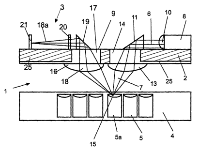
Figure 1 depicts a measuring device 1 (not shown to scale)
having a fluorescence spectrometer 3 that is mounted
integratively on a substrate board 2, an array 4 of, for
example, six reaction vessels 5 positioned one behind the
other, and the corresponding paths of rays 6,7. At this point,
it is mentioned that both a plurality of spectrometers 3, as
well as a plurality of reaction vessels 5 may be positioned
one behind the other, side-by-side, or in a matrix-type
configuration. Spectrometer 3 has a light source 8, which is
mounted as a miniaturized laser diode 8 on top side 9 of
substrate board 2. A beam-shaping aperture optics 10 may be
mounted on laser diode 8.
Provided, in addition, on top side 9 of substrate board 2 is a
beam-reflecting prism 11 and an illuminating optics 13 mounted
at an appropriate position on bottom side 12 of substrate
board 2. Illuminating optics 13 is preferably designed as an
elliptical focusing lens 13 and includes an aberration
correction.
Above focusing lens 13, substrate board 2 has a
light-transmitting region 14, preferably a passage 14.
In this context, focusing region 15 (Figures l, 2) of focusing
lens 13 used for focusing illuminating beam 10 has a diameter
of about 1 ,um. In accordance with the present invention, in
integrated spectrometer 3, a collective lens 16 is mounted on
bottom side 12 of substrate board 2 in such a way that it
borders on focusing lens 13: Above collective lens 16,
substrate board 2 has a passage 17 for leading through a
fluorescence light beam 18 radiated from reaction vessel 5a.
NY01 466733 v 1 7 REVISED PAGES
CA 02388350 2002-04-16
Through this pick-up lens 16 mounted next to focusing lens 13,
fluorescent light 18, which is excited by illuminating beam 7,
is picked up at a different angle having a high numerical
aperture.
An illuminating beam 7 emanating from laser diode 8 of
spectrometer 3 is directed via beam-reflecting prism through
passage 14 of substrate board 2. Illuminating beam 7 is
focused at a reaction vessel 5a, which, for instance, has only
a volume of approximately 10-6 1 and which is positioned in
reaction vessel array 4 facing bottom side 12 of substrate
board 2.
Since the two paths of rays 7, 18 only have region of focus 15
in common, the reaction space is defined by the intersection
volume of illuminating light beam 7 and of fluorescence light
beam 18 inclined thereto, and is definitively set by the
design. In the specific embodiment according to Figures 1 and
2, the received fluorescence light 18 is directed by
collective lens 16, via a prism 19 working with total
reflection, to a dispersive element 20, preferably a
diffraction grating.
A plurality of such reaction vessels 5 is preferably combined
in a series-type array 4. A chemical reaction in reaction
vessel 5a is verified on the basis of a fluorescent emission
of one or more attached molecules.
Focusing lens 13 and collective lens 16 are microlenses having
surfaces which are capable of being transilluminated and have
axes of about 10 - 100 ,um.
In one especially preferred specific embodiment of the present
invention, dispersive element 20 is implemented as a phase
grating 20 having a free-standing design.
Fluorescent light 18 is diffracted by phase grating 20 in
NYOi ass~33 v ~ 8 REVISED PAGES
w,
CA 02388350 2002-04-16
dependence upon the wavelengths, in various directions at a
detector array 21. It is advantageous to select the spacing
between individual detectors 22 of detector array 21 in
coordination with diffraction grating 20, such that a detector
22 is impinged on, at any one time, in focused fashion by one
single, well defined wavelength of fluorescent light 18a.
Detectors 22 are preferably designed as free-standing
structures and are constructed in an electron beam-induced
deposition, where they are placed with a precision of a few nm
on a prepared electrical connecting structure in the form of
printed conductors 23. In this context, detectors 22 are
preferably designed as photoresistors, having a length of
about 2 ,um and a diameter of about 100 - 200 nm. The
photoresistors are preferably fabricated from nonocrystalline
material of, for instance, Au or Pt, in a dielectric carbon
matrix.
By positioning the resistors to the exact location and
producing the grating constant of phase grating 18, within the
scope of the present invention, the detectable wavelengths are
definitively set, as they are known from tracer molecules that
are excitable to emit fluorescence.
Through the use of phase grating 18, all intensity is directed
in one order of diffraction, preferably in the first order of
diffraction. In one especially preferred use of an echelette
phase grating having a selected design, all diffracted light
is directed in only one of two orders of the same order
number, so that the maximum fluorescence light signal is
obtained. For this, the first order is advantageously
selected.
Two spectrometers 3 may also be preferably positioned
side-by-side, i.e., in parallel. By adding a beam splitter 24,
from light source 8, preferably designed as a laser diode, is
split into two beam components to supply parallel spectrometer
NY01 466733 v ~ 9 REVISED PAGES
CA 02388350 2002-04-16
3.
In an especially preferred exemplary embodiment according to
Figure 3, two pairs of spectrometers 3 are each supplied with
radiation via a beam sp utter 24. In this context, also in the
case of the illustrated multiple pair-wise array of such
spectrometer pairs, the particular path of rays is produced
with the aid of beam splatters from the light beam emanating
merely from one light source.
It should also be mentioned that the device according to
Figures 2 and 3 is equivalent to that in Figure 1 and,
therefore, identical or equivalent parts are provided with the
same reference numerals By using integrative technology and
computer-controlled design, it is possible to manufacture the
device having parallel-functioning spectrometers 3 in large
quantities. This is advantageously accomplished by a multiple
beam splitting. For this, beams 6', 6" emanating from a
central beam splatter 24 are directed into two spectrometer
branches 25, 26. Provided, in turn, in each of the two
spectrometer branches 25, 26, in accordance with the present
invention, is a beam splatter 24' and 24", respectively. Beam
splatters 24' and 24", respectively, each supply two
spectrometers of the type shown in Figures 1 and 2.
Within the framework of the present invention, optical
components, such as lenses, prisms and/or gratings, are
constructed in a computer-controlled process, using a dry
resist technique and/or an electron beam-induced deposition.
In accordance with the present invention, the positioning of
the optical components is adjustable to an accuracy of within
a few nm.
The device according to the present invention, i.e., the
spectroscopy device manufactured in accordance with the method
of the present invention, may essentially be used as follows.
NY01 466733 v 1 10 REVISED PAGES
CA 02388350 2002-04-16
A chemical reaction is verified by the motion, essentially the
Brownian motion of the fluorescing molecules attached to at
least one of the participating reagents. In the process, the
molecular velocity in the reaction product is measured. In
accordance with the present invention, this is accomplished by
adjusting the measured displacement via an illuminating path
predefined by the optics. The time duration of the
fluorescence radiation corresponds to the time for which
detectors supply a signal induced by monochromatic fluorescent
light 18a. In this context, fluorescent light 18a is
decomposed by dispersive element 20 according to the
wavelength.
From the thus ascertained velocity, the existence of a
specific chemical reaction, i.e., the level of already
converted reagents may be determined.
Spectrometer 3 or an array of spectrometers may also be
assigned to an array of reaction vessels 4. In an array 4 of
up to a few hundred reaction vessels 5, 5a, for instance,
every second one may have a spectrometer 3 facing opposite it,
so that every second reaction vessel 5a may be read out
simultaneously. The two arrays may also be moved in relation
to one another, and, in this manner, reaction vessels 5 that
are not yet measured may be positioned in front of the
corresponding spectrometers 3 for measuring purposes.
It is then possible to query the desired reaction via a
detector read-out. The detector read-out may also be
preferably performed as a computer-controlled operation. In
one preferred specific embodiment of the present invention,
the detectors used, in which an optically sensitive material
is a 0-dimensional electron gas, yield a high upper critical
frequency. In these materials, only hopping, as a mechanism of
electrical conduction, determines the signal transfer. In a
0-dimensional electron gas of this kind, the energy levels are
separated at room temperature to a greater degree than the
NYO1 466733 v 1 11 REVISED PAGES
CA 02388350 2002-04-16
thermal energy kBT, kg being the Boltsmann constant. Thus, at
room temperature (>27 meV), the photoresistors preferably used
are especially low-noise.
The fluorescence radiation is verified by reading out the
photocurrent at detector 22 designed as a photoresistor. By
introducing an absorber layer 25 to bottom side 12 of
substrate board 2, it is beneficially achieved that only the
intensity striking into the lens aperture attains detector
array 21 of spectrometer 3. It is likewise achieved that
adjacent detectors 22 are not influenced. Due to the small
size of detectors 22, a plurality of detectors 22, preferably
up to a few hundred, may be implemented in one array 21.
The present invention is not limited to the described
exemplary embodiments, which may be modified in a multiplicity
of ways.
The multiple illumination and spectrometry systems may also
each be equipped with only one detector 22 for the light of
the wavelength of a specific fluorescing substance subsequent
to diffraction grating 20. Thus, all reactions, which are able
to be marked by only one specific fluorescent molecule, may be
analyzed using this system. The result is a considerable
simplification of the evaluation electronics, since only one
photoresistor is set up and employed at a specific location.
In this type of detector array 21, a limited resolution of
spectrometer 3 suffices, which lowers the quality required of
focusing 15 and of diffraction grating 20.
In accordance with the present invention, the light supply and
the array of dispersive elements 20 may be positioned such
that they are inclined from above toward substrate board 2, or
inclined away from this board. This means that laser diode 8
is secured to a separate holder over the board, but
beam-reflecting prism 11 for deflecting beam 6 is eliminated
and is only replaced by a reflection-reducing layer for entry
NY01 466733 v ~ 12 REVISED PAGES
CA 02388350 2002-04-16
of the light into substrate board 2. In this context,
diffraction grating 20 is mounted such that it lies directly
on board surface 9 and likewise on a reflection-reducing layer
to improve passage of fluorescent light 18. Array 21 of
photodetectors 22 is then likewise mounted on a separate board
above substrate board 2, requiring a special, precise
adjustment of laser diode 8 and of detectors 22.
To achieve an especially high spectral resolution in the
fluorescent light, it is also possible to use a combination of
prisms and gratings, or also other spectrometers made, for
example, of photonic crystals.
Laser diode 8 emitting the exciting light may be provided as
an individual diode in the spectrometer or in the device. In
this context, it is also conceivable to integrate laser diode
8 monolithically with substrate board 2. The laser diodes may
be battery-operated.
Also implicit in the present invention is that, in a parallel
configuration of a plurality of spectrometers 3 or devices,
substrate boards 2 are kept separately from one another, or
also connected to one another. In addition, the present
invention also includes the implementation of a plurality of
spectrometers 3, which are able to be positioned in a series-
or matrix-type array on a shared substrate board. ,
It is also provided for a laser diode 8 to be mounted as a
power diode having beam-splitting multiple couplers in
multimode waveguide technology, on central substrate board 2
supporting the prisms and lenses. In addition, it is provided
to distribute the light with equal intensity into individual
reaction vessels 5, 5a. Using this technique, it is possible
to simultaneously supply 1, 2, 4, 8, 16, etc. parallel devices
NYO1 466733 v 1 13 REVISED PAGES
CA 02388350 2002-04-16
or spectrometers with light of the same intensity, thereby
multiplying the rate at which the reactions to be analyzed are
able to be assessed.
The detector read-out may also take place, for example, via an
infrared signal output. To improve the signal-to-noise ratio,
a preferably miniaturized chopper may be provided in the
illuminating beam, in order to operate, for example, a lock-in
amplifier mounted on the detector side.
Combining, replacing, or supplementing the described specific
embodiments with other additional, generally customary optical
components, such as excitation light sources or detectors and
the like, is to be considered, moreover, as included within
the scope of the present.
Finally, it is understood that the individual features of the
present invention may also be used in combinations other than
those described or presented.
NYO~ as6~33 v ~ 14 REVISED PAGES