Note: Descriptions are shown in the official language in which they were submitted.
CA 02388654 2002-04-19
WO 01/47098 PCT/US00/41494
-1-
Description
ENERGY CONSERVING MOTOR CONTROLLER
Technical Field
This invention is generally related to control of AC electric machines, and in
particular to power factor controllers for single phase and three phase
induction motors.
Background Art
It is well known that operation of an AC induction motor at substantially less
than its full rated load becomes more and more inefficient in the use of
electrical energy as the
power factor of the load, which varies inversely with the load, increases.
Conventional
methods and controllers for reducing energy consumption of AC induction motors
have been
developed or proposed. One class of such devices and methods uses a measure of
the power
factor of the AC machine, e.g., an AC induction motor, to generate a control
signal used for
adjusting the AC power delivered to the motor. In order to maintain sufficient
rotor "slip" for
operation with a relatively low power factor and best efficiency, the control
signal is adjusted
to reduce the average power applied to the motor during light loading.
Other conventional systems and methods include: ( 1 ) controllers and methods
which, instead of relying on an accurate time base, use counters based on
imprecise time bases
or are subject to drift with temperature, voltage or load or, which are in
turn subject to
2 0 interruption by external signals or interference, typically resulting in
inefficient or
inappropriate control actions; (2) systems that are susceptible to severe back-
EMF effects or
other electromagnetic interference generated in the motor or in the controller
itself which may
substantially interfere with accurate power factor sensing and control or an
inability to process
sensor parameters or generate unambiguous control signals because of the high
interference
levels that are present; (3) systems and methods that only work well when the
motors
connected to the controller are in good condition, are correctly wired to the
power source
and/or the controller or do not have significant phase winding irregularities
imbalances or
mechanically unbalanced loads which typically results in an inability to
properly compensate
CA 02388654 2002-04-19
WO 01/47098 PCT/US00/41494
-2-
or adjust the power factor or, in some cases, motor failure; (4) systems that
must be manually
adjusted to accommodate individual application conditions which are labor
intensive and
costly, and may fail to provide optimum adjustment because the range of
adjustment is
limited; (5) setting desired power factor parameters by hand or setting
average power factors
that once set, are fixed, and at best only approximate the potential
efficiency improvement that
is desired from the system; and (6) systems or methods which required complex
control
circuitry or modification to the motors in order to provide efficient control
which also tends
to increase the cost of manufacturing, installing the systems or of using
them.
Disclosure of the Invention
The energy conserving controller of the present invention dynamically matches
energy use by an AC induction motor to the load on the motor. First and second
SCRs are
provided, each having a respective gate and connected in parallel with each
other in opposing
polarities between a first node and a second node, for each phase of the
applied AC voltage.
The first node is connected to a source of the applied voltage, the second
node is connected
to at least one winding of the motor. A trigger generator is coupled to the
respective gates of
the SCRs, to the applied voltage and to the motor winding for controlling each
of the first and
second SCRs responsive to the respective timing of sensed zero crossing events
of the AC
voltage and the AC current in the motor winding corresponding to the applied
AC voltage.
Further, the first and second SCRs are alternately triggered into a conductive
state during each
2 0 alternation of the applied AC voltage and are alternately inhibited from
the conductive state
for an interval in time proportional to a measured difference in time between
the time the AC
voltage across the motor winding passes through a first zero-crossing and the
time the
corresponding AC current in the motor winding passes through a second zero-
crossing,
wherein the measured difference is determined as the time difference between
successive first
2 5 and second interrupts are coupled to the trigger generator and compared
with a continuously
running time base.
According to another aspect of the present invention, the gate drive for the
SCRs coupled between the first and second nodes is selectively opened and
closed by the
control signal provided by the trigger generator.
CA 02388654 2002-04-19
WO 01/47098 PCT/US00/41494
-3-
In another aspect of the present invention, the trigger generator comprises a
first input for sensing the AC voltage applied to the motor winding; a second
input for sensing
the AC current in the motor winding corresponding to the AC voltage applied to
the motor
winding; an output for providing a trigger control signal for controlling each
of the first and
second SCRs; and a control device including a continuously running time base
that is
responsive to the first and second interrupts corresponding respectively to
the first and second
inputs for generating the trigger control signal.
In yet another aspect of the present invention, the control device comprises a
measurement system for measuring the elapsed time between the first and second
interrupts
occurring in a select phase of the applied AC voltage and for calculating the
product of the
elapsed time and a predetermined factor. The control device includes the
capability for
generating a trigger control signal, within a first time interval following
the zero- crossing of
the current in the motor during the select phase of the AC voltage, wherein
the trigger control
signal has a duration substantially equal to the product of the elapsed time
and the
predetermined factor; and wherein further the first and second gate drive
circuits are disabled
for the duration of the trigger control signal.
Brief Description of the Drawing
For a more complete understanding of the present invention and its advantages,
reference is now made to the following description taken in conjunction with
the
2 0 accompanying drawing figures in which:
FIGURE 1 illustrates a block diagram of an embodiment of a three phase power
factor controller according to the present invention;
FIGURE 2 illustrates a simplified schematic of a power factor controller for
a representative phase according to the present invention;
FIGURE 3A illustrates the voltage and current waveforms of a representative
phase of the electrical power connected to the motor winding;
FIGURE 3B illustrates interrupt waveforms corresponding to the voltage sense
zero-crossing signals in the representative phase of the applied voltage;
FIGURE 3 C illustrates interrupt waveforms corresponding to the current sense
3 0 zero-crossing signals in a representative phase of the applied voltage;
CA 02388654 2002-04-19
WO 01/47098 PCT/US00/41494
-4-
FIGURE 3D illustrates a waveform of the trigger control signal derived from
the zero-crossing signals applied to an SCR gate drive circuit;
FIGURE 4A illustrates each phase of the voltage and current waveforms
coupled to a three-phase motor wherein one of the phases of the voltage and
current
waveforms are shown with the clipped region of the waveforms providing the
reduced power
delivered to the motor;
FIGURE 4B illustrates waveforms corresponding to the current sense zero-
crossing signals of the particular phase of the voltage and current
illustrated in FIGURE 4A;
FIGURE 4C illustrates a trigger control signal that results from the detection
of the zero-crossing events illustrated in FIGURE 4B that is applied to the
gate drive circuit
of the first and second SCRs;
FIGURE 5 illustrates a flowchart of the main routine of the program for
operating the CPU of the trigger generator of the present disclosure; and
FIGURE 6 illustrates a flowchart for the interrupt routine in which the zero-
crossing information is utilized to generate a trigger control signal to
control the power
delivered to the motor by the power factor controller of the present
invention.
Best Mode for Carrying Out the Invention
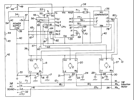
Referring now to FIGURE 1, there is shown a block diagram of one
embodiment of a three phase power factor controller 10 according to the
present invention.
2 0 Each phase control section in FIGURE 1 is identified with a respective
phase by the
designation ~,, ~z, and ~3. The individual phase control sections are coupled
to and
controlled by the combination of a CPU and a composite comparator also shown
in FIGURE
1 along with a DC power supply to provide the operating voltages for the CPU
and the
composite comparator. Also shown in FIGURE 1 are incoming connections from the
three
phase AC power source operating at either 50 or 60 Hz as well as the outgoing
connections
to a three phase induction motor that is controlled by the power factor
controller according to
the present disclosure.
In the power factor controller 10 shown in FIGURE l, the incoming phases of
the three phase AC voltage are coupled respectively along lines L~, L~ and L;.
Each phase
3 0 control section includes terminals labeled L,, M~, I,, T and V~~. Line L,.
identified by
CA 02388654 2002-04-19
WO 01/47098 PCT/US00/41494
-5-
reference number 11, is coupled to a node 14 and the L, terminal of the phase
control section
~~. Phase control section ~~ is identified by reference number 13. Similarly
L,, identified as
line 18, is coupled to node 21 and to the L~ terminal of phase control section
20 (i.e., ~2).
Similarly line L3, identified as line 25, is coupled to a node 28 and to
terminal L3 of phase
control section 27 (i.e., ~3). In a similar fashion an AC voltage line is
coupled from terminal
M, on phase control section 13 to a node 16 and there along line 12 to
terminal M, for
connection to the three phase induction motor. Line 19 is coupled from
terminal M2 of phase
control section 20 to node 23 and there along line 19 to terminal M2 of the
motor. Line 26
couples the M3 terminal of phase control section 27 to node 30 and along line
26 to terminal
M3 of the three phase induction motor. There is also shown in FIGURE 1 a
connection from
the incoming AC voltage source to an earth ground terminal identified by the
conductive path
32 to the symbol identifying earth ground.
Continuing with FIGURE 1, in the three phase system of the present disclosure
wherein typically each of the three phases is balanced with respect to earth
ground, one of the
phase voltages is selected as the ground reference for the control circuitry
of the power factor
controller system shown in FIGURE 1. In FIGURE 1 the designated control
circuit ground
reference is connected to line L, at node 14. This control circuit ground is
shown by the
ground symbol connected to node 33 which is connected to node 14 in FIGURE 1.
It will be
appreciated that this control circuit ground coupled to node 33 is a floating
ground with
2 0 respect to earth ground in that it assumes the potential that exists on
line L, at any given
moment in time. This occurs because all of the control circuitry that operates
at a low voltage
is referenced to this particular control circuit ground at node 33 and each of
the control or
sensing signals are coupled to the phase control sections through isolation
circulation. The
isolation circuitry, besides isolating the high voltage AC from the Iow
voltage control sections
2 5 also removes any DC component from the signals that are coupled between
the control section
and the individual phase control sections.
Each of the phase control sections comprises a pair of SCRs for switching the
AC voltages to the motor windings. Also included are the gate drive circuitry
for controlling
the switching of the SCRs, zero-crossing sense circuitry for obtaining timing
information
3 0 related to the zero-crossing event of the respective AC voltage and
current phases, and the
aforementioned high voltage / low voltage isolation present in the control and
sense signal
CA 02388654 2002-04-19
WO 01/47098 PCT/US00/41494
-6-
lines. Thus, for example, phase control section 13 includes terminals for
connections to AC
voltage line L,, to the motor voltage line M,, also to a DC voltage V~~ to
part of the isolation
circuitry, to terminal T for trigger control signals and from terminal I, for
sensing the zero-
crossing of the current signal. Similarly phase control section 20 has
terminals for connections
to line Lz, to line MZ to the motor, from the DC voltage supply V~~, to
terminal T for the
trigger control signal and from terminal I, for the current sense zero-
crossing signal. Finally,
phase control section 27 similarly includes terminal L3 connected to AC
voltage line L3,
terminal M3 connecting the phase control section to the motor winding terminal
M3, as well
as terminals for V~~, the trigger control signal T and terminal I3 for the
current sense zero
crossing signal for ~3.
It will also be observed that connected to nodes 14, 21 and 28 are harmonic
suppression capacitors connected between the identified node and earth ground,
respectively
capacitor 15, capacitor 22 and capacitor 29. In similar fashion, nodes 16, 23
and 30 are also
coupled to earth ground through harmonic suppression capacitors identified as
capacitor 17,
capacitor 24 and capacitor 31. Each of these harmonic suppression capacitors
absorbs
transient energy in the form of line voltage spikes, turn-off transients or
other high frequency
noise that may exist on the respective AC voltage lines L~, L, and L3 or on
the leads to the
motor windings M,, M, and M3.
Continuing with FIGURE 1, there is shown a DC power supply 34 which
2 0 obtains AC voltage coupled from line L; at node 41 through line 42,
capacitor 43, resistor 44
and node 49 to node 50 which is tied to terminal VS of the.control section CPU
35. Capacitor
43 serves as a high pass filter along with resistor 44. Also coupled to node
49 is resistor 48
connected to control section ground which, in conjunction with resistor 44,
provides a voltage
divider for stepping down the amplitude of the incoming AC voltage on line L3
to nodes 49
and 50. Terminal VS is provided to sense the zero-crossing of the AC voltage
applied to the
motor. Also coupled to node 50 is a two-pole, single-throw switch S,
identified by wiper
terminal 51 and terminals 52 and 53.
Terminal 53 is coupled to the AC input of power supply 34. Power supply 34
includes a rectifier circuit for converting the incoming AC voltage to an
unregulated DC
3 0 voltage. The unregulated DC voltage is applied to a voltage regulator
circuit within power
supply 34 and provides +5 volts DC at output terminal 37 which is connected to
line 38 to
CA 02388654 2002-04-19
WO 01/47098 PCT/US00/41494
_7_
distribute the +5 volts to the various V~~ terminals of the operating portions
of the control
circuitry. Power supply 34 is connected from its common terminal 39 along line
40 to node
33 coupled to the control circuit ground. Line 40 is further coupled to
various other portions
of the control circuitry to provide the ground connection to the VSS terminals
of the control
sections as well as to individual portions of the circuitry related to the
control section.
Switch S,, described previously, couples the stepped down AC voltage to either
terminal 53 to the power supply 34 or to a terminal 52 which provides a keep-
alive bias
current to the isolating circuits for the trigger control signal. This keep-
alive current is
necessary to maintain the gate control circuitry affecting the SCRs in an
active condition.
When power is supplied to the circuit, the gate drive current required for
turning on each of
the SCRs in their respective alternations of the incoming AC voltage is
provided to enable
them to turn on when the anode becomes positive with respect to the cathode.
Thus terminal
52 of switch S, is coupled through resistor 55 to node 56 and thence along
line 57 to the
trigger terminal T of the phase control section 13.
Similarly, terminal 52 of switch S, is coupled through resistor 58 to node 59
and thence along line 60 to terminal T of the phase control section 20. And,
terminal 52 of
switch S, is coupled through resistor 61 to node 62 and thence along line 63
to terminal T of
phase control section 27. CPU 35 further includes one triggering terminal for
each of the
phase control sections described previously. The Trig 1 trigger control signal
from the CPU
2 0 is provided to node 56. The Trig2 terminal of CPU 35, which is the trigger
control signal for
...... _ the phase control section 20, is applied to node 59. Similarly the
Trig3 trigger control signal _
is supplied from the Trig3 terminal of CPU 35 to node 62.
Continuing with FIGURE 1, there are also shown in CPU 35 three input
terminals corresponding to each of the three current sense zero-crossing
signals. These signal
2 5 terminal inputs are identified respectively as interrupt # 1 (Int 1 ),
interrupt #2 (Int2) and
interrupt #3 (Int3). Signals representing the zero-crossing event of the
respective AC currents
in each of the phase windings are obtained from the respective phase control
sections.
Beginning with phase control section 13, an output terminal at I~ provides for
sensing the zero-
crossing of the motor winding current and applying that signal to terminal I,
of comparator 36.
3 0 Comparator 36 represents a composite of the individual comparator sections
for each of the
phase windings. Each comparator section includes a separate input filter and
separate
CA 02388654 2002-04-19
WO 01/47098 PCT/US00/41494
_g_
comparator section for its respective current sense line. Each of the
comparators is referenced
to a common voltage reference circuit. The comparator and filter circuits will
be described
herein below in conjunction with FIGURE 2.
To summarize the operation, a current sense signal line is coupled from
terminal I, of phase control section 13 to terminal I, of comparator 36, a
current sense line is
coupled from terminal IZ of phase control section 20 to terminal I, of
comparator 36 and a
current sense line is coupled from terminal I3 of phase control section 27 to
terminal I3 of
comparator 36. Correspondingly, the signal paths following the processing
performed by the
comparator section 36 are coupled along similarly identified lines to the CPU
35. Thus,
Terminal I, of comparator 36 couples the current sense signal for phase
control section 13
along line 75 to Intl of CPU 35. Similarly, current sense line I, from
comparator 36 is applied
respectively along line 76 to Int2 of CPU 35 and from terminal I3 of
comparator 36 along line
77 to Int3 of CPU 35. Composite comparator 36 receives DC voltage from power
supply 34
along line 38 and also is tied to the control circuit ground at node 33.
Continuing further with FIGURE 1, there are several other features providing
additional functions of the power factor controller according to the present
disclosure. CPU
35 includes an internal oscillator that is controlled by a crystal 68 coupled
to terminals X1 and
X2 of CPU 35. This crystal controlled oscillator serves as the continuous time
base for
operating the CPU 35 as well as providing a reference for making accurate time
interval
2 0 measurements. Terminal B7 of CPU 35 is coupled to the control circuit
ground through a
resistor 69 and a light emitting diode (LEDI 70 to provide an indication of
the operating status
of the power factor controller according to the present disclosure. The LED 70
has three
states: steady OFF indicates CPU 35 is off; steady ON indicates CPU 35 has
been reset and
is executing a start-up delay; and a flashing LED 70 indicates the circuit 13
is fully functioning
2 5 to control the energy applied to the motor.
Several address lines of CPU 35 are also shown in FIGURE 1. Terminal RAO
is shown connected through resistor 71 and a jumper block 72 which in turn is
coupled to
control circuit ground at line 40. The jumper block 72 provides for connecting
the resistor 71
to ground to change the turn-on delay for the CPU 35 from approximately 30
seconds to
3 0 approximately 45 to 60 seconds in this illustrative example. Address line
RA2 is coupled
through node 64 and resistor 65 to DC voltage line 38. Node 64 is coupled
through variable
CA 02388654 2002-04-19
WO 01/47098 PCT/US00/41494
-9-
resistor 81 to the control circuit ground at line 40. Address line RA3 is
coupled through node
66 and resistor 67 to DC voltage line 38. Node 66 is coupled through variable
resistor 82 to
the control circuit ground at line 40. These variable resistors allow for
adjusting the duration
of the trigger control signal, i.e., the clip region, as described herein
below during the
description of FIGURE 6.
In operation, each of the phase control sections 13, 20 and 27 of FIGURE 1
provides for controlling the flow of AC current along a respective AC voltage
line through the
SCR switches contained in the phase control section. For example, the AC
voltage applied
to terminal L, along line 1 ~ and to terminal L, of phase control section 13
is coupled through
the internal SCRs when they are in a conducting condition and therealong from
the terminal
M~ along line 12 to one terminal M, of the three phase induction motor. As
will be described
herein below, the control of the SCRs within the phase control section enables
adjustment of
the voltage applied to the motor in accordance with the power factor for that
particular phase
winding of the motor that is developed by the action of the CPU 35 in the
control section. The
control section develops a trigger control signal for controlling the
respective gate drive circuit
for each of the SCR pairs within each phase control section as a function of
the time interval
that occurs between the moment of the zero-crossing of the AC voltage applied
to the motor
and the AC current flowing in the motor winding for that particular phase of
the applied
voltage. The zero-crossing of the AC voltage is sensed at a respective
terminal VS of CPU 35
2 0 as described previously.
In the illustrative embodiment described herein it is usually not necessary to
provide the same filtering and comparator circuits for the voltage sense zero-
crossing signal
because it is derived from an incoming phase of the AC voltage and is less
likely to include
a large noise component or be subject to phase shift variations as is the
current sense zero-
2 5 crossing signal. It is possible in certain applications, however, that
some signal processing
circuit to ensure a clean, noise-free voltage sense signal may be required.
Continuing with the operation of FIGURE l, the zero-crossing of the AC
current for the phase control section 13 is sensed along the line 75 coupled
to Intl terminal of
CPU 35 after being processed by the comparator 36 to provide a clean,
accurately timed and
3 0 full logic level sense signal. Each of the respective phase control
sections is controlled by its
own trigger control signal developed from measuring its own power factor by
determining the
CA 02388654 2002-04-19
WO 01/47098 PCT/US00/41494
-10-
time elapsed between the respective zero-crossing events for each of the motor
winding
phases. The effect of a trigger control signal upon the SCRs is to disable the
gate drive circuit
for a period of time related to the particular power factor of the load
measured during the
alternation of the AC voltage previous to the phase of the voltage being
controlled. This is
described in detail herein with reference to FIGURES 4A, 4B and 4C.
Referring now to FIGURE 2, there is shown a simplified schematic of a power
factor controller for one phase of the applied AC voltage according to the
present disclosure.
The figure shows the basic internal structure of a phase control section along
with the control
circuit or trigger generator that is responsive to and supplies control
signals for the phase
control section. Coupled between a first node 101 and a second node 102 are a
first SCR 113
and a second SCR 114. The anode of an SCR 113 is connected to the first node
101 and the
cathode of SCR 113 is connected to the second node 102. Similarly, the anode
of an SCR 114
is connected to second node 102 and the cathode of SCR 114 is connected to
first node 101.
The gate terminal of SCR 113 is connected to a node 105 and the gate terminal
of SCR 114
is connected to a node 106. Also connected between first node 101 and second
node 102 is
the series combination of a resistor 115 and a capacitor 116. First node 101
is connected to
a node 103 and the second node 102 is connected to a node 104.
A gate drive circuit comprising the parallel combination of a resistor 117 and
a steering diode 119 is connected between node 103 and node 105. Similarly, a
gate drive
2 0 circuit comprising the parallel combination of a resistor 118 and a
steering diode 120 is
connected between.node 104 and node 106. The cathode of steering diode 119 is
connected
to node 105 and in turn to the gate terminal of SCR 113. Similarly, the
cathode of steering
diode 120 is connected to node 106 and in turn to the gate terminal of SCR
114. Node 105
is connected along a line 111 through a resistor 139 to one terminal of an
optocoupler 136 at
one side of an optically sensitive triac 138 within optocoupler 136.
Similarly, node 106 is connected along a path 112 to the opposite side of
optically sensitive triac 138 within optocoupler 136. Optocoupler 136 is
located within a
trigger generator 130 to be described herein below. The applied AC voltage is
applied to
terminal L~ which is coupled to node 161 and coupled therefrom along a line
107 to node 103.
3 0 Node 103 is further coupled along a line 109 to node 141 within trigger
generator 130. Node
161 is further coupled to earth ground through a harmonic suppression
capacitor 121. The AC
CA 02388654 2002-04-19
WO 01/47098 PCT/US00/41494
-11-
voltage terminal for supplying AC current to the motor winding controlled by
the phase
control section shown in FIGURE 2 is supplied from node 104 along line 108
through a node
162 to terminal M, of the motor winding coupled to the phase controller shown
in FIGURE
2. Node 162 is coupled through a harmonic suppression capacitor 122 to earth
ground.
In operation, the representative phase control section illustrated in FIGURE 2
provides for controlling the switching of applied AC voltage to the respective
motor winding
connected to the phase control section. SCR 113 and SCR 114 are each connected
in series
with the applied AC voltage such that the applied voltage supplies the
necessary anode-to-
cathode voltage for the respective SCR to be triggered into conduction at the
onset of either
alternation of the applied AC voltage. Then an appropriate current is supplied
to the
respective gate which is enabled to conduct by the polarity of the AC voltage
that appears
between first node 101 and second node 102. Thus, SCR 113 is enabled to
conduct when the
first node 1 O l is at a positive potential with respect to second node 102
and gate drive current
arrives via the gate drive circuit coupled between nodes 103 and 104.
Similarly SCR 114 is enabled to conduct in the presence of a suitable gate
drive current when the polarity of the applied voltage of first node 1 O 1 is
negative with respect
to second node 102. The respective gate drive current for SCR 113 is supplied
through the
first gate drive circuit (comprising resistor R17 and steering diode 119)
during the time when
the first node 101 is positive with respect to second node 102. Similarly, the
gate drive
2 0 necessary for causing SCR 114 to go into conduction is supplied through
second gate drive
circuit (comprising resistor 118 and steering diode 120) via node.l 06 to the
gate of SCR 114
and second node 102 and node 104 have a positive potential with respect to
first node 1 O1 and
node 103.
As will be described in detail herein below, the optically sensitive triac 138
2 5 within optocoupler 136 is always in a conducting state except when caused
to turn off by the
trigger control signal from CPU 35 and impressed across LED 137 within
optocoupler 136.
The effect of the triac 138 and the series resistor 139 is to maintain both
nodes 105 and 106
and therefore the first and second gated drive terminals G, and G, at a
common, balanced
potential with respect to first node 101 and second node 102. This assures
that each gate
3 0 terminal will be biased to be driven into conduction when the respective
SCR is forward
biased by the applied AC voltage. When triac 138 is conducting, resistor 139
and the
CA 02388654 2002-04-19
WO 01/47098 PCT/tJS00/41494
-12-
conducting triac provide a path for the gate voltage of each respective SCR to
be biased with
respect to the polarity of the applied voltage opposite that of the respective
SCRs anode
terminal. Without the conductive paths through resistor 139 and a conducting
triac 138, this
reference path is absent and the respective gate is allowed to float;
therefore it cannot then
obtain a potential that is positive with respect to the cathode voltage of the
respective SCR.
Thus, when the triac 138 is caused to go into a non-conducting state, the
balancing path
through resistor 139 is opened. This action allows the gates to float and
inhibits the gate drive
to the respective SCR, thus interrupting the application of the applied AC
current to the motor
winding. The series combination of resistor 115 and capacitor 116 connected
between first
node 1 Ol and second node 102 provides a snubbing action to limit the turn off
transients of
each SCR as it enters a non-conducting state.
Continuing with FIGURE 2, the circuitry within the trigger generator 130 will
now be described. There is shown an optocoupler 133 which contains a
bidirectional light
emitting diode pair 134 on its input side and a photo transistor 135 on its
output side. The
emitter of the photo transistor 135 is coupled to the control circuit ground.
The collector of
photo transistor 135 within optocoupler 133 is coupled to a node 142. A
resistor 143 is
coupled from the node 142 to the DC supply voltage through a node 151 to the
supply voltage
line 38 (not shown in FIGURE 2). A resistor 144 is coupled between node 142
and control
circuit ground. Node 142 is further coupled to a node 146 through a resistor
145, and node
2 0 146 is coupled to the positive input of a comparator 148. Node 146 is
coupled to control
circuit ground through a capacitor 147, thus forming a.low pass filter for
filtering any noise
present on the signal appearing at node 142.
The negative input terminal of comparator 148 is coupled to a voltage
reference
source at a terminal 149. In the illustrative embodiment shown herein, the
reference voltage
2 5 provided at terminal 149 may be on the order of +2.5 volts DC. The output
of comparator 148
is coupled to a node 150 which in turn is coupled to the current sensing input
of the CPU 132
in the trigger generator 130. CPU 132 in FIGURE 2 is functionally the same as
CPU 35 in
FIGURE 1 in the illustrative embodiment. Node 150 is also coupled through a
resistor 152
as a pull-up resistor connected through a node 151 to the supply voltage at
line 38.
3 0 Returning now to optocoupler 133 in FIGURE 2, it will be seen that the
bidirectional light emitting diode 134 is coupled on one side to line 110 to
node 104 in the
CA 02388654 2002-04-19
WO 01/47098 PCT/US00/41494
-13-
phase control circuit. The opposite side of bidirectional light emitting diode
134 is coupled
through resistor 140 to node 141 which is connected to the source of AC
voltage applied to
the circuit. In operation, when the voltage applied to both sides of the
bidirectional light
emitting diode 134 is at the same potential, neither of the bidirectional LEDs
will be able to
conduct and therefore they are both off and no light is being emitted that can
be picked up by
the photo transistor 135. This condition arises whenever there is no current
flowing between
the L, terminal and the M, terminal because both SCRs are in a non-conducting
state, which
condition arises when the current between first node 101 and second node 102
is in a zero-
crossing condition. At this instant the bidirectional LEDs 134 turn off and
remove the drive
signal from the base of phototransistor 135 causing its collector to rise to
the applied DC
voltage. As this voltage rises past the level of the voltage reference value
present at terminal
149, the comparator 148 changes state and provides a full swing logic signal
to the current
sense input of the CPU 132.
Continuing now with the trigger generator 130 illustrated in FIGURE 2, it will
be seen that the light emitting diode I 37 within optocoupler 136 receives its
operating current
from the DC voltage supply through a resistor 154 and a node 153 to the anode
of LED 137.
The cathode of LED 137 is connected to control circuit ground. Node 153 is
further coupled
to the trigger output of CPU 132. In operation, as previously explained, a
trigger control
signal supplied by CPU 132 causes node 153 to fall to logic low which turns
off LED 137
causing the output circuit comprising triac 138 and resistor 139 to become an
open circuit.
,. Also shown in trigger generator 130 is a voltage sense circuit wherein the
voltage sense
terminal of the CPU 132 is coupled through node 155 and resistor 160 to a
terminal 157 of a
wiper of a single-pole double-throw switch. The other side of the wiper is
shown connected
to a terminal 158 which is also coupled to node 141 and in turn coupled to the
applied AC
voltage at terminal L,. Terminal 158 of the switch is shown labeled as single
phase and a
terminal 159 is shown labeled as three phase with an arrow indicating that it
is to be used
when the switch is set for three phase operation.
In the three phase operation condition, the voltage sense line is connected to
line L3 to obtain an AC voltage zero-crossing signal. In either case the AC
voltage zero-
3 0 crossing signal is coupled from terminal 15? through a resistor 160 and a
node 155 to the
voltage sense terminal of CPU 132. Node 15~ is coupled to ground through a
resistor 156.
CA 02388654 2002-04-19
WO 01/47098 PCT/US00/41494
-14-
Resistor 156 and a resistor 160 form a voltage divider to step down the
relatively high value
of the applied AC voltage to a level that can be tolerated by the input port
of CPU 132. Due
to the step down divider action of resistors 156 and 160, and the fact that
the line voltage
applied to the VS terminal is very small - typically less than +5 volts peak-
to-peak - as well as
being AC coupled (via C3) no other isolation is required in the VS sense line.
In operation, the
CPU 132 calculates the time difference between the arrival of a zero-crossing
signal at the
voltage sense terminal and the zero-crossing signal arriving at the current
sense terminal to
determine a measure of the power factor of the load coupled to the motor. CPU
132 uses this
time measurement to calculate the duration of the trigger control signal that
is supplied at the
trigger terminal of CPU 132. The relationship of the zero-crossing signals
supplied to the
voltage and current sense terminals and the development of the trigger control
signal will be
described herein below with respect to FIGURES 3 and 4.
Referring now to FIGURE 3A, there are illustrated the voltage and current
waveforms of a representative phase of the electrical power connected to the
motor winding.
The current waveform 202 is shown lagging the voltage waveform 201, as is
typical in the
winding of an induction motor. One cycle of the voltage waveform 201 and of
the
corresponding current waveform 202 beginning with the zero-crossings occurring
at times 204
(voltage) and 205 (current) respectively is shown in FIGURE 3A. These
waveforms show the
effect of the control circuit described previously in conjunction with FIGURE
2 with respect
2 0 to the reduction of the applied voltage to the motor. The voltage to the
motor is, in effect.
turned off for a brief portion of each positive and negative alternation of
the applied ar'
voltage.
The amount of time the applied AC voltage is turned off during each
alternation
is proportional to the power factor that is calculated from the time interval
that occurs between
2 5 two successive interrupts corresponding to the zero-crossing of the
respective applied voltage
and applied current through the motor winding. Thus, in FIGURE 3A the OFF
portion of the
applied voltage appears as interval 203 corresponding to the pulse width of
the trigger control
signal (to be described) which is generated based on the elapsed time between
the voltage
zero-crossing at time 204 and the current zero-crossing at time 205. The
trigger control signal
3 0 ends at time 206. At the end of the trigger control signal the voltage
rises to its nominal peak
value and returns to its sinusoidal waveform.
CA 02388654 2002-04-19
WO 01/47098 PCT/US00/41494
-1 S-
The same effect is seen in the negative alternation wherein following the
voltage zero-crossing interrupt at a time 207 and the current zero-crossing
interrupt at time 208
the trigger control signal is once again applied to the SCR gate drive circuit
and causes the
voltage waveform 201 to be turned off for a portion of a time before being
restored to the
sinusoidal waveform shown in FIGURE 3A. In this way, by turning off the
applied voltage
for brief controlled periods during each alternation of each cycle, the
average voltage applied
to the motor winding is reduced to compensate for the large power factor that
develops when
the motor is lightly loaded. This reduction in the average power delivered to
the load tends
to bring the power factor back into an efficient range.
During each alternation of the applied voltage, the lagging current
corresponding to the applied voltage is also reduced to zero during the OFF
interval of the
applied voltage beginning, as with the voltage. at the time that the current
passes through zero.
It will also be noted in FIGURE 3A, that when the current begins to flow in
the motor winding
after the end of the OFF period, the current does not instantaneously rise to
the value that it
would have been without the applied AC voltage being switched off by the
trigger generator;
rather it rises in approximately sinusoidal fashion and once again crosses
zero at a time 208
corresponding to the amount by which the current waveform lags the voltage
waveform. The
reason for this is that the current in an inductance is not able to change
instantaneously but
rather requires some amount of time to charge the inductance of the winding.
The same effect.
2 0 of course, is repeated in each successive alternation of the current in
the windings
corresponding to the applied AC voltage.
Referring now to FIGURE 3B. there is illustrated a series of interrupt pulses
corresponding to the voltage sense zero-crossing signals in the representative
phase of the
applied voltage. In FIGURE 3B a very brief negative transition occurs at every
point in time
2 5 that the applied AC voltage waveform passes through zero. This negative
transition is shown
in the form of a brief negative going pulse which returns to the high logic
level almost
immediately following the zero-crossing event. Thus, the waveform 211 includes
for each
zero-crossing event a negative transition 213 to a logic low level and returns
via a positive
transition 214 to the high logic level of waveform 211 until the next zero-
crossing event of the
3 0 applied AC voltage. Thus is developed a negative pulse train that has a
repetition rate of 120
cycles per second for 60 cycle AC power or in the case of 50 cycle AC power,
the repetition
CA 02388654 2002-04-19
WO 01/47098 PCT/US00/41494
-16-
rate would be 100 Hz. These interrupts are developed within the CPU 35 in
response to the
voltage VS that appears at the voltage sense terminal of CPU 35.
Referring now to FIGURE 3C, there is illustrated a series of interrupt pulses
corresponding to the current sense zero-crossing signals in a representative
phase of the
applied voltage. The wave shapes in FIGURE 3C appear very much as the
interrupt wave
shapes of FIGURE 3B with the exception that the trailing edge of the pulse
corresponding to
a trigger event is delayed during the period that the current is zero because
both SCRs are off
until the end of the gate control and the applied voltage is once again
applied to the motor.
Thus the interrupt signal corresponding to the current zero-crossings normally
has a logic high
level until a zero-crossing event occurs whereupon the signal undergoes a very
rapid negative
transition to a low logic level and, unless there is a trigger control signal
present will almost
immediately return along a very rapid positive transition to the nominal high
level logic signal.
If, however, a trigger control signal is applied, then the zero-crossing
signal that
is sensed at the motor winding terminal remains at a low logic level until the
end of the trigger
control signal. In FIGURE 3C, there is shown a succession of three trigger
control periods,
one for each of three successive alternations of the applied AC voltage
corresponding to the
waveform illustrated in FIGURE 3A. In FIGURE 3C, a high logic level 215
becomes a
negative transition 217 at the instant of a zero-crossing event of the current
in the motor
winding and falls to a low logic level 216 until it is restored along a
positive transition 218 to
2 0 the nominal high le~~el 215. The low logic level corresponding to the
period that a trigger
control signal is active is shown as low logic level 219 in FIGURE 3C.
FIGURE 3D illustrates the trigger control signal which, during the period that
it is active, closely resembles the interrupt waveform corresponding to the
zero-crossing events
of the applied voltage and current during the period the trigger control
signal is active. Again,
2 5 a high logic level 220 is followed by a negative transition 222 to a low
logic level 221 where
the signal remains until the end of the trigger control signal is followed by
a rising transition
223 to the nominal high logic level 220. It will be observed by comparing
FIGURE 3B and
FIGURE 3C that the negative transition of the sense signals provide the
interrupts and the
information needed to approximate the power factor of the motor. The elapsed
time between
3 0 the zero-crossing events is obtained by subtracting the earlier time of a
voltage zero-crossing
CA 02388654 2002-04-19
WO 01/47098 PCT/US00/41494
_17_
event from the later time of the current zero-crossing event and using this
interval of time to
calculate the duration of the trigger control signal that is needed to reduce
the average applied
AC voltage to the amount necessary to bring the power factor for a light load
back within a
reasonable and efficient range. As previously described, the trigger control
waveform shown
in FIGURE 3D controls the opening of the SCR gate circuit comprised of 8139
and the triac
138 within optocoupler 136 shown in FIGURE 2. When the SCR gate circuit is
opened, the
SCR enters a non-conducting or blocking state.
Referring now to FIGURE 4A, there are illustrated both a voltage waveform
250 and a current waveform 251 for a three phase system wherein one cycle of
the phase three
1 o voltage waveform 250 shows the effect of the power factor controller upon
the voltage and
current waveforms for that particular cycle. The zero-crossing events for the
applied voltage
occur at times 254 and 256 in FIGURE 4A; similarly the times for the
occurrence of the zero-
crossing events of the current waveform occur respectively at times 255 and
257. The
difference in time occurring between the respective voltage and current zero-
crossing
interrupts is used to calculate the duration of the control period for each
alternation of the
applied voltage waveform. This control period, sometimes also called a clip
region 252, in
the positive and clip region 253 in the negative of the phase three voltage
waveform 250,
represents the time during which the AC voltage is interrupted or removed from
the motor
windings to which that phase three is connected.
2 0 Once again it is seen in FIGURE 4A that the resulting current waveform 251
in phase. three takes on a sinusoidal characteristic between..the end of the
trigger control or
clip region 252 and the subsequent zero-crossing event at a time 257 that
follows the applied
AC voltage zero-crossing according to the particular amount of phase lag
between the current
and voltage for that winding of the motor. FIGURE 4B in this illustrative
example shows the
2 5 zero-crossing sense signals for both the voltage and current in the
particular phase three
illustrated in FIGURE 4A. A voltage sense signal 258 for phase three is
followed in time by
a current sense signal 259 for phase three. Similarly, in the succeeding
alternation in the
negative direction a voltage sense signal 260 for phase three is shown
followed by a current
sense signal 261 for phase three.
3 0 Referring now to FIGURE 4C, there is shown the trigger control signal for
phase three corresponding to the zero-crossing sense signals illustrated in
FIGURE 4B. It can
CA 02388654 2002-04-19
WO 01/47098 PCT/US00/41494
-18-
be readily seen that the timing of the trigger control signal begins at the
onset of the current
zero-crossing signal and continues for the clip region 252 until the trigger
control signal once
again returns to the high logic level at a transition 263 for the positive
going alternation of
phase three of the applied voltage waveform 250 shown in FIGURE 4A. Similarly
the trigger
control signal for the negative alternation of phase three is shown also in
FIGURE 4C with a
negative transition 264 followed after the clip region interval at a
transition 265 back to the
logic high nominal level.
A simple relationship may be pointed out as shown in FIGURE 4C wherein the
time between the voltage and current zero-crossing events - and the
corresponding interrupts -
is identified as 4T3 and the duration of the clip region which follows the
current zero-crossing
interrupt is identified as 0~3. OT3 corresponds to the power factor of the
load on the motor
winding and 4~3 corresponds to the duration of the clip region, i.e., the
control period of the
same alternation for which the power factor measurement has been made. These
two variables
will be seen to be related by a simple factor depending upon the kind of motor
being
controlled.
Referring now to FIGURE 5 there is illustrated a simplified flowchart
illustrating the main program routine for the power factor controller of the
present disclosure.
The flow begins at a block 302 where the program starts when power is applied
to the system
or when the system has been reset. The flow proceeds to a block 304 where the
CPU runs
2 0 through the routine for setting up all of the registers in the CPU, for
firing all of the SCRs of
the phase control sections so that power may applied to the motor, and for
setting the preset
timer values. Thereupon the flow proceeds to a block 306 where the routine
reads the startup
delay input to the system and causes the status LED to become illuminated
continuously. The
startup delay referred to in block 306, as described herein above, is the
delay set by the jumper
2 5 72 which connects resistor 71 to the control circuit ground. This delay,
with the jumper
removed, is on the order of 30 seconds; with the jumper in place the delay is
lengthened to the
range of 45 to 60 seconds. In a block 308, the routine checks to be sure the
delay has been
fully executed and proceeds to a block 310 where the routine sets the
interrupts and sets the
status LED to a flashing condition indicating that the CPU is controlling the
operation of the
3 0 power factor controller.
CA 02388654 2002-04-19
WO 01/47098 PCT/US00/41494
-19-
Following block 310, the main program routine proceeds to a block 312 and
the principle operations of the CPU are performed in a loop that begins with
clearing the
watchdog timer in a block 312 followed by a flow of the routine to a block 314
to check the
analog to digital converters for clip adjustments that have been calculated
and if clip
adjustments are found then the CPU stores the clip adjustments for later use
during the
appropriate interrupts to be discussed herein below. Clip adjustments are
changes to be made
to the duration of the trigger control signal. Following execution of the
principle program
steps, the main program routine proceeds from a block 314 to a decision block
316 wherein
it checks for whether or not the power has been turned off to the system; if
the result is
affirmative then the flow proceeds to a block 318 where the routine ends and
the system is off.
If, however, the power is still on, then the flow returns to the step
illustrated
in a block 312 to clear the watchdog timer and the main program routine
proceeds through its
principal functional activities. As was previously stated, an interrupt may
occur at any time
during the operation of the main program routine. The CPU for the power factor
controller
of the present disclosure has been programmed to service these interrupts as
they occur during
the principle program loop represented by blocks 312 and 314. The interrupts
that are serviced
by the main program routine are described in the flowchart illustrated in
FIGURE 6 to be
described herein below.
Refernng now to FIGURE 6 there is illustrated the routine for processing the
2 0 interrupts that may occur in the power factor controller of the present
disclosure. The routine
..._ . is entered at a block 320 when an interrupt ~~ccurs. followed by a
block 322 wherein the
routine saves the program counter and the accumulator to the stack for use
when the
interrupts) have been serviced and the flow returns to the main program. The
interrupt
routine of FIGURE 6 provides for servicing three kinds of interrupts essential
to the operation
2 5 of the power factor controller. These three kinds of interrupts are
represented by decision
blocks 324, 326 and 328. Decision block 324 represents the occurrence of an
interrupt for a
signal representing a voltage zero-crossing event which, in the illustrative
embodiment, occurs
when the AC voltage of line 3 crosses through the zero point as sensed by an
interrupt pin.
If the interrupt was not of this type then the flow proceeds to decision block
326 where the
3 0 routine determines whether the interrupt that is present is a timer
interrupt, that is, a timer
which operates at 128 times the power line frequency in the illustrative
example.
CA 02388654 2002-04-19
WO 01/47098 PCT/US00/41494
-20-
This timer provides for dividing the power line frequency period into 128
equal slices to provide a time base for the operation of the power factor
controller to determine
the timing associated with measuring the zero-crossing interval, OT, and
calculating the
duration 0~ of the trigger control signal (e.g., 266 in FIGURE 4C) generated
by the CPU 132
in the trigger generator 130 as shown in FIGURE 2. If the interrupt being
serviced in block
326 is not a timer interrupt, then the flow proceeds to a block 328 where the
routine
determines whether the interrupt corresponds to the occurrence of a zero-
crossing event of the
current in the motor. If the result of this determination is negative, then
the flow proceeds to
a block 330 where the interrupt routine restores control to the program
counter and the
accumulator and, in a block 332. returns to the main program.
Returning now to decision block 324, if the interrupt that is present
represents
the zero-crossing of the AC voltage at line 3, then the flow proceeds along
the path labeled
"yes" to a block 334 where the internal counter begins counting from zero
toward the time
when an interrupt representing the zero-crossing of the current occurs in
order to measure the
interval 0T between the voltage zero-crossing event and the current zero-
crossing event for
line 3 of the applied AC voltage. When the current zero-crossing event occurs,
the flow
proceeds back to the entry of decision block 324 which is also identified as
point A in the
interrupt routine and a decision is made in decision block 324 as to whether
the interrupt that
just occurred is a voltage zero-crossing event in line 3. In this particular
case, the flow will
2 0 proceed from decision block 324 to decision block 326 because the
interrupt that just occurred
was not a voltage zero-crossing event in line 3.
In decision block 326 the routine checks for whether the interrupt that just
occurred was caused by the internal timer and in this case the result is
negative so the flow
proceeds to a block 328 where a determination is made as to whether the
interrupt that just
occurred is a current zero-crossing event. In this case, the result is
affirmative and the flow
proceeds along the path labeled ''yes" to a second level of decision blocks
352, 362 and 368.
In decision block 352, the routine determines whether the interrupt
representing a zero-
crossing event of the current occurred in line 3. If the determination is
affirmative, then the
flow proceeds along the path labeled "yes'' to a block 354 where the routine
calculates the
3 0 duration of the clip region which. as previously described, is the same as
the duration of the
trigger control signal (e.g., 266 in FIGURE 4C) to be generated by CPU 132.
CA 02388654 2002-04-19
WO 01/47098 PCT/US00/41494
-21-
The duration 4~ of the trigger control signal(e.g., 266 in FIGURE 4C)
determines the duration of the clip region in a one-to-one relationship. The
trigger control
signal, by causing the disabling of the gate drive circuits for the SCRs in
each phase control
section causes the SCR in the respective alternation to enter a non-conductive
state during the
period of the clip region. Thus the clip region represents the period when the
AC voltage to
the motor winding is interrupted. The duration of this clipped region of the
AC voltage is a
function of the amount of phase lag of the current in the motor winding
relative to the voltage
zero-crossing event for the associated phase of the AC voltage applied to the
motor winding.
In the illustrative embodiment, the relationship of the trigger control signal
duration in general
is some predetermined multiple of the duration OT of the time elapsed between
the voltage
zero-crossing event and the current zero-crossing event for that particular
phase.
For example, in motors operating on 240 volts AC, three phase, the duration
of the trigger pulse bears a one-to-one relationship with the duration of the
zero-crossing
interval 0T. Thus, in this example, the length of time the voltage waveform
will be
interrupted is equal to the elapsed time occurring between the zero-crossing
events for the
particular phase being controlled by the trigger control signal. This one-to-
one relationship
may be modified by a clip adjustment which is added to the clip duration or
the pulse width
of the trigger control signal pulse 0~ to advance or retard the trailing edge
of the trigger
control signal. The clip adjustment will be described herein below. Similarly,
in another
2 0 example for three phase motors operating on 480 volts AC, the duration of
the clip region is
determined by dividing .the zero-crossing interval AT by two and adding a
clip.acliustment to
advance or retard the trailing edge of the trigger control signal for that
particular type of motor.
The clip adjustment made to the duration ofthe clip region, i.e., the pulse
width
of the trigger control signal 0~ is determined from the setting of
potentiometers in the trigger
generator connected to designated pins of CPU 35 shown in FIGURE 1. The
designated pins
of CPU 35 for these potentiometer connections are RA2 and RA3. The
potentiometers form
the lower half of a voltage divider connected between the +5 volt V~~ line 38
and the control
circuit ground at line 40. RA2 at CPU 35 is connected to node 64 which is the
junction
between resistor 65 and potentiometer 81. Potentiometer 81 provides for
setting the clip
3 0 adjustment for 240 VAC motors in this illustrative example. Similarly in
RA3 of CPU 35 is
connected to node 66 which forms the junction of resistor 67 and potentiometer
82.
CA 02388654 2002-04-19
WO 01/47098 PCT/US00/41494
-22-
Potentiometer 82 provides for setting the clip adjustment for 480 VAC motors.
When potentiometer 82 is set to its maximum resistance, no additional time is
added to the
duration of the zero-crossing interval 4T to set the pulse width of the
trigger control signal
(266). As the resistance of potentiometer 82 is reduced, the voltage at pin
RA3 at CPU 35 is
also reduced which has the effect of advancing the occurrence of the trailing
edge of the
trigger control signal, that is, to shorten the pulse width of the trigger
control signal. When
potentiometer 81 is set to its minimum resistance, the voltage at pin RA2 is
set to its minimum
value. As the resistance of potentiometer 81 is increased, the effect is to
retard the timing of
the trailing edge of the trigger control signal; that is to lengthen the pulse
width of the trigger
control signal.
Continuing with the two examples for 240 volt AC three phase motors and 480
volt AC three phase motors described above, the predetermined settings for
determining the
clip adjustment to the pulse width for the respective trigger control signals
for these two types
of motors was described. It will be appreciated that these two examples are
illustrative of just
two of numerous possible arrangements in the control of the pulse width for
controlling the
power delivered to each phase of a three phase machine or even to a single
phase machine may
be determined. Thus, whether the adjustment is called a clip adjustment or by
some other
term, these examples are illustrative of the variety of ways in which the
pulse width of the
trigger control signal may be determined for any particular application.
2 0 Returning now to FIGURE 6 at a block 356, the routine sets the clip region
duration and adjusts it according to the setting of the potentiometers R1 and
82 external to
CPU 35 as shown in FIGURE 1. The flow then proceeds to a block 358 where the
routine sets
the pulse width of the trigger control signal for phase three to the clip
duration as adjusted in
the block 356. The flow then proceeds to a block 360 which represents the
application of the
trigger control signal to the SCR gate drive circuit within the phase three
control section (27
in FIGURE 1 ) to cause the phase control section 27 to clip line 3, that is,
to inhibit the gate
drive circuitry within the phase control section 27 so as to cause the SCR
corresponding to the
particular alternation of the applied AC voltage to turn off following the
zero-crossing event
until the gate drive is restored by the trailing edge of the trigger control
signal. From block
3 0 360, the flow then proceeds along the line to the point A which, as
previously described,
returns the routine to the input to decision block 324.
CA 02388654 2002-04-19
WO 01/47098 PCT/US00/41494
-23-
Referring now to block 352 of FIGURE 6, in the event that the current zero-
crossing event did not occur with AC line 3, then the flow proceeds along the
path identified
as "no" to decision block 362 where a determination is made whether the
particular phase to
which the current zero-crossing event is associated is phase two. If the
result of the
determination in block 362 is affirmative then the flow proceeds to a block
364 where the clip
duration for phase two is set equal to the clip duration plus adjustment as
determined in block
356. It is important to note that the clip duration adjustment that occurs in
block 356 is
utilized to determine the clip duration for each of the phases of the motor
winding. Thus, once
it is determined for phase three in block 356, then the same value is used for
succeeding
phases until the value is updated or recalculated in block 356 when the
interrupt routine is
servicing the time interval between the voltage zero-crossing and the current
zero-crossing for
phase three.
Returning now to block 364, after the clip duration for phase two is set equal
to the clip duration calculated in block 356, then the flow proceeds to a
block 366 whereupon
the trigger generator outputs a trigger control signal for phase two and
causes the inhibition
of the gate drive circuitry for the corresponding SCR in the phase control
section for phase two
as previously explained for block 360. After generating the trigger control
for phase two, then
the flow proceeds again to point A where it returns to the input decision
block 324. Returning
now to decision block 362, if it was determined that the current zero-crossing
event did not
2 0 occur with phase line two, then the flow proceeds along the path
identified as "no" to a
decision block 368 which makes a determination as to whether the current zero-
crossing event
occurred in phase one.
If the result is negative, the flow proceeds along a path identified as "no"
to
point A where it returns to the input of decision block 324. If, however, the
result of the
determination in block 368 is affirmative, then the flow proceeds to a block
370 where the
routine sets the clip duration for phase one equal to the clip duration
determined in block 356
and then proceeds to a block 372 where the trigger control signal for phase
one is generated
having the duration determined in block 370, causing the SCR corresponding to
the particular
alternation of the applied AC voltage to become non-conductive, thus blocking
the application
3 0 of the AC voltage to the respective motor winding for the duration of the
pulse width of the
CA 02388654 2002-04-19
WO 01/47098 PCT/US00/41494
-24-
trigger control signal. Thereupon, the flow proceeds to point A and back to
the input of
decision block 324 to again evaluate the next interrupt.
Returning now to decision block 326 which determines whether the interrupt
received was caused by the internal timer and the case where the resulting
determination was
affirmative, the flow proceeds to block 336 whereupon the counter which counts
the
increments of time that make up the duration of the clip region, that is, the
pulse width of the
trigger control signal, is reloaded with the reload value corresponding to the
clip duration plus
any adjustment that was provided. After the timer is reloaded, the flow
proceeds to block 338
where the routine increments or decrements the counters as needed toward the
end of the clip
region. While counting, the interrupt routine checks to determine which clip
region is being
counted and whether that particular count for that clip region has reached
zero corresponding
to the end of the clip region. Thus, beginning with decision block 340, the
routine determines
whether the counter for clip region three has reached zero and if the result
is "yes" in block
342, the counting is halted marking the end of the clip region which is
equivalent to the
trailing edge of the trigger control signal pulse. The trigger generator then
outputs a positive
transition to end the clip region for that alternation.
The flow then proceeds to point A where the routine returns back to the input
to block 324. Returning now to block 340 where the decision to determine
whether the
counter for clip 3 region three has reached zero and the answer is negative
then the flow
2 0 proceeds to decision block 344 which seeks to determine whether the clip
region being
.. ~. processed is for phase two and if so, whether the. counter has reached
zero. If the answer is
affirmative, then the flow proceeds to block 346 where the clip region count
is halted at zero
and the trigger generator is signaled to end the clip region by outputting a
positive transition
trailing edge to the trigger control signal pulse for phase two. Again, the
flow then proceeds
2 5 to point A and back to the decision block 324.
Returning to decision block 344, if the clip region being processed is not
phase
two or the count has not reached zero then the flow proceeds to decision block
348. In block
348 the determination is made as to whether the phase being processed is phase
one and the
counter for this phase has reached zero; if the result is "no," then the flow
proceeds to point
3 0 A and back to the input of block 324 to continue processing the interrupt
routine. If however,
the determination is made in decision block 348 that the present clip region
is determined to
CA 02388654 2002-04-19
WO 01/47098 PCT/US00/41494
-25-
be phase one and it has reached zero then the processing flows along the "yes"
path to block
350 where the counter for counting down the time value for clip region one is
halted and the
trigger generator outputs a positive going trailing edge and the clip region
for phase one
whereupon the flow continues back to point A and returns to the input of
decision block 324
to continue processing subsequent interrupts.
Industrial Applicability
The energy conserving power factor controller 10 of the present invention is
intended for controlling electrical power delivered to AC motors that are
operated under
varying mechanical load conditions, for example single phase and three phase
AC induction
motors that drive pumping units which extract oil from underground deposits.
Such pumping
units are alternately loaded by pumping rods and opposing counterweights twice
each
pumping cycle. Moreover, twice each cycle the two opposing loads balance and
the pump
drive motor is thus unloaded twice each cycle. The power factor controller 10
continuously
adjusts the power delivered to the pump drive motor to maintain optimum
efficiency and
economy between peak minimum and maximum values presented by the constantly
changing
load.
Although the preferred embodiment has been described in detail, it should be
understood that various changes, substitutions and alterations can be made
therein without
departing from the spirit and scope of the invention as defined by the
appended claims.