Note: Descriptions are shown in the official language in which they were submitted.
CA 02388662 2002-04-15
WO 01/37427 PCT/US00/41227
Description
DIGITAL FREQUENCY MONITORING
TECHNICAL FIELD
This invention relates to pulse monitoring
systems and in particular to systems for detecting the
pulse width of received signals.
BACKGROUND ART
Transmitted digital signals need their pulse
widths to remain within a prescribed tolerance in order
for the receiving circuitry to be able to ascertain the
data content of the transmitted signals. A transmitted
digital signal may become distorted by frequency response
effects of the transmitting medium, by loss of energy
over distance, electromagnetic interference, etc.
With reference to Fig. 1, two sample pulse
sequences are shown. Both begin with a logic low and
transition to a logic high. In the case of a logic low,
TLmin denotes the minimum allowed pulse length of a logic
low pulse and TLmax denotes the maximum allowed pulse
length for a logic low pulse. In order for a receiving
circuit to accept a logic low to high transition, the
incoming pulse low signal should transition within a
window of time defined by the difference of TLmax and
TLmin. This window of time is defined as logic low
transition window, W0, in Fig. 1. Similarly, a logic
high pulse also needs to have a pulse length defined by a
minimum logic high pulse length, THmin, and a maximum
logic high pulse length, THmax. In order for a logic
high to low transition to be accepted, the transition
should occur within a window of time defined by the
difference of THmax and THmin. This window of time is
defined as a logic high transition window, W1. As shown
with the two sample pulse sequences of Fig. 1, the time
CA 02388662 2002-04-15
WO 01/37427 PCT/US00/41227
-2-
windows WO and W1 need not be the same for different
applications, although they typically should remain
constant within a single application.
The receiving circuit includes a pulse
detecting sub-circuit to observe the pulse length of
received pulse signals. Prior art pulse detecting
circuit typically observe only one of the logic high or
logic low pulse of a received signal, but not both. This
means that the pulse detecting circuit cannot determine
the signal period of the received pulse signal, and thus
cannot observe shifts in the signal's frequency.
Frequency shifts in a received pulse signal can therefore
lead to undetected errors.
Prior art pulse detecting circuits typically
use two one-shot circuits to determine if a received
signal is valid for a predetermined transition window.
Both one-shot circuits are typically triggered on the
leading edge of an received pulse signal. A first one-
shot circuit issues a first pulse having a length equal
to the minimum pulse length requirement, and the second
one-shot circuit issues a second pulse having a length
equal to the maximum pulse length requirement. At the
end of the second pulse, the received signal is compared
with the first and second pulse. If the length of the
received pulse does not lie within the first and second
pulse, then no detection signal is issued and the
received pulse signal is ignored. One shot-circuits,
however, are difficult to control or adjust in integrated
circuitry. Additionally, they do not provide for a
simple way of adjusting the required transition window
for different applications.
This prior art approach can also slow down a
system since the pulse detecting circuit waits for the
lapse of the maximum pulse length before verifying the
received pulse signal. In effect, it waits the maximum
amount of delay time for each received pulse signal even
06-10-2001 ~ U S004122 i
CA 02388662 2002-04-15
- 3-
if the received pulse signal transition earlier and do
not require any additional wait time. U.S. Pat.
3,735,271 to Leibowitz shows a pulse width detecting
circuit that does not wait for the maximum allowable
pulse length before testing for a valid received pulse
signal. The '271 circuit, however, requires three one-
shot circuits and adds a delay to each received pulse
signal. This added delay may actually cause additional
errors. Assuming the circuit receives a pulse signal
having a pulse length slightly shorter than the minimum
require pulse length, the added pulse delay introduced by
'271 may actually cause the circuit to think that the
received signal did meet the minimum pulse length
requirement.
' Additionally, other prior art pulse detecting
circuits include Japanese Patent Abstract JP 01175409A
which discloses a signal discriminating device for pulse
signals and Japanese Patent Abstract JP 59005737A which
discloses a pulse width detecting circuit.
It is an object of the present invention to
provide a pulse detecting circuit that observes both a
received pulse signal's pulse length and its frequency.
It is another object of the present invention
to provide a pulse detecting circuit that observes both
logic high and logic low pulse of a received pulse
signal.
It is yet another object of the present
invention to provide a pulse detecting circuit that lends
itself to simple integration onto an IC circuit and that
permits its allowable pulse transition windows WO and W1
to be independently, or jointly, adjusted from inside and
from outside the IC circuit.
SUMMARY OF THE INVENTION
The above objects are met in a pulse detection
circuit that uses a pair of linear voltage ramp
AMENDED SHEET
06-10-2001 U S0041227
CA 02388662 2002-04-15
-3A-
generators and a reference voltage source for
establishing a preferred pulse length window for a
received pulse signal. The present pulse detection
circuit monitors both the positive duty cycle and the
S negative duty cycle of a received pulse signal.
AMENDED SHEET
CA 02388662 2002-04-15
WO 01/37427 PCT/US00/41227
-4-
Therefore, it can detect frequency shifts in the received
pulse signals. If a positive or negative duty cycle is
found to be either too short or too long, it is
categorized a "bad" duty cycle and an error signal is
issued that disables the internal circuitry of a chip.
If the duty cycle lies within a predetermined time
window, i.e. a preferred pulse transition window, it is
categorized as a "good" duty cycle. If an error signal
is issued due to encountering a bad duty cycle, the
internal circuitry of the chip remains disabled until two
consecutive good duty cycles are observed. When the
present pulse detection circuit receives two consecutive
good pulses, i.e. good high pulse following a good low
pulse, or a good low pulse following a good high pulse,
it issues an enable signal to re-enable the internal
circuitry of the chip.
The present duty cycle monitoring circuit
includes two monitoring sub-circuits. A first sub-
circuit monitors the positive duty cycle of an incoming
pulse signal, and a second sub-circuit monitors the
negative duty cycle of the incoming pulse signal. Since
the positive and negative duty cycles are monitored by
separate sub-circuits, the present pulse detection
circuit can support different preferred pulse transition
windows for positive duty cycles and for negative duty
cycles. For the sake of brevity, only the first sub-
circuit for monitoring a positive duty cycle described
here. The circuit structure for the second sub-circuit
is similar to the first sub-circuit and is discussed in
detail in the best mode description below.
A preferred pulse transition window, W1, for a
"good" positive duty cycle is first defined. This pulse
transition window is established by means of a slower
linear voltage ramp and a faster linear voltage ramp
working in unison. As time passes, the voltage
difference between the slower and faster linear voltage
CA 02388662 2002-04-15
WO 01/37427 PCT/US00/41227
-5-
ramps increases, and this voltage difference becomes a
measure of the a duty cycle duration. A desired duration
window is established by noting the voltage value of the
slower linear voltage ramp when the voltage difference
between the slower and faster linear voltage ramps
becomes representative of the desired pulse transition
window. This noted voltage value becomes a reference
voltage to which an incoming clock is compared. In other
words, the length of a pulse transition window can be
adjusted or shifted in time by changing the reference
voltage or by adjusting the slope of the linear voltage
ramp generators. The reference voltage may be generated
from within the circuit or may be supplied from a source
external to the circuit.
As logic state of an incoming clock changes
from low to high, the slower and faster voltage ramps are
reset and re-triggered. A first comparator is used to
compare the rising voltage value of the faster voltage
ramp with the reference voltage. The first comparator
signals when the faster voltage ramp rises above the
reference voltage. A second comparator is used to
compare the rising voltage value of the slower voltage
ramp with the same reference voltage. The second
comparator signals when the slower ramp rises above the
reference voltage. The received pulse signal is within
the desired pulse length while only while the faster
voltage ramp is above the reference voltage and the
slower voltage ramp is below the reference voltage. If
either comparator indicates that these conditions are not
true, then the duty cycle of the incoming clock is
outside the desired window and it is categorized as a
"bad" duty cycle.
Upon the trailing edge of the received pulse,
the output of the comparators is analyzed and the result
stored in a first register. A second register stores the
result of the previous received pulse. The state, good
CA 02388662 2002-04-15
WO 01/37427 PCT/US00/41227
-6-
or bad, of the current pulse is compared with the state,
good or bad, of the previous pulse. If the state the
current pulse is bad, then a disable signal is issued.
If the state of the current pulse is good, but the state
of the previous pulse is bad, then the disable signal
remains issued. If the state of the current pulse and
the previous pulse are both good, then an enable signal
is issued.
Additionally, included is an initiation circuit
that maintains a constant disable signal during the first
few received pulse signals at start-up. This gives the
internal circuitry time to achieve a known state before
being enabled by the pulse detecting circuit.
BRIEF DESCRIPTION OF THE DRAWINGS
Fig. 1 illustrates the variation in pulse width
of a digital signal.
Figs. 2 & 3 show the relationship of between
two linear voltage ramps.
Fig. 4 is a functional block diagram of the
present invention.
Fig. 5 shows exemplary voltage versus time
plots illustrating how the present invention identifies
when a pulse signal transistions within a preferred
transition window.
Fig. 6 is a more detailed functional diagram of
a pulse monitoring circuit in accord with the present
invention.
Fig. 7 is a circuit implementation of the
present invention.
BEST MODE FOR CARRYING OUT THE INVENTION
The present pulse monitoring circuit uses two
pulse detecting sub-circuit to monitor both the positive
duty cycle an the negative duty cycle of incoming pulse
signals. By monitoring both the positive duty cycle and
CA 02388662 2002-04-15
WO 01/37427 PCT/US00/41227
the negative duty cycle, the present pulse monitoring
circuit can determine if the overall signal period of a
received pulse signal is within predetermined minimum and
maximum period time lengths. By noting shifts in the
period of received pulse signals, the present pulse
monitoring circuit can likewise make note of shifts in
the frequency of received pulse signals.
With reference to Fig. 2, each of the two pulse
detecting sub-circuits uses a pair of linear voltage
ramps to measure the pulse duration of a received logic
pulse signal. Plots VoTLf and VoTLs show exemplary
outputs of two linear voltage ramp generators used for
observing a received logic low pulse. The logic low
pulse detecting sub-circuit includes a slower linear
voltage ramp generator producing output VoTLs and a
faster linear voltage ramp generator producing output
VoTLf. Both the faster and slower linear voltage ramps
are reset upon receipt of a logic low pulse and begin to
ramp up at a predetermined voltage/second rate. This
rate may be adjusted by adjusting the strength, i.e.
current sourcing capability, of the individual linear
voltage ramp generators. A reference signal Vref sets
the maximum allowable time TLmax for a logic low pulse
and also sets the minimum allowable time TLmin for a
logic low pulse. The TLmin time limit is set at the
intersection of Vref with VoTLf, and the TLmax time limit
is set at the intersection of Vref with VoTLs. As shown,
the minimum time duration TLmin for a logic low pulse is
determined by the faster linear voltage ramp VoTLf, and
the maximum time duration TLmax for a logic low pulse is
determined by the slower linear voltage ramp VoTLs. The
difference between TLmax and TLmin defines the time
boundaries for a desired logic low transition window W0.
The with of WO may be adjusted by raising or lower Vref,
or by changing the slope of one or both of VoTLf and
VoTLs. If a received logic low pulse transitions to a
CA 02388662 2002-04-15
WO 01/37427 PCT/US00/41227
_g_
logic high within the transition window defined by W0, it
is categorized as a "good" received pulse, but if it
transitions outside W0, then it is categorized as a "bad"
received pulse.
With reference to Fig. 3, exemplary plots of
linear voltage ramps VoTHs and VoTHf used for monitoring
the logic high pulse length of a received pulse signal is
shown. Signals VoTHs and VoTHf begin to ramp up upon
receipt of a logic high pulse. As before, the
intersection of the faster voltage ramp VoTHf and
reference voltage Vref establishes the minimum time
duration TLmin for a pulse width, in this case a positive
pulse width. Similarly, the intersection of Vref and the
slower linear voltage ramp VoTHs establishes the maximum
duration of a positive pulse with. The difference of the
maximum allowable pulse duration TLmax and the minimum
pulse duration TLmin establish the boundaries for a
desired logic high to logic low transition window W1. In
the present preferred embodiment, preferred transition
window Wl is shorter than W0, but this is not crucial to
the invention. In many cases, it may be desirable for W1
and WO to define a similar time window. It should be
noted, however, that both WO of Fig. 2 and W1 of Fig. 3
are a function of the same reference voltage Vref.
Although it is not critical to the invention that both WO
and W1 be responsive to the same reference signal Vref,
this is preferred since it simplifies simultaneous
control of both WO and W1. The width of Wl may also be
adjusted by adjusting one or both of VoTHf and VoTHs.
Thus the present pulse detecting circuit can
detect time deviations in both logic high and logic low
cycles, of a received pulse sequence. This permits it
detect not only when a logic pulse is outside its
preferred transition window, but also when its period,
and therefore its frequency, shifts beyond acceptable
limits.
CA 02388662 2002-04-15
WO 01/37427 PCT/US00/41227
_g_
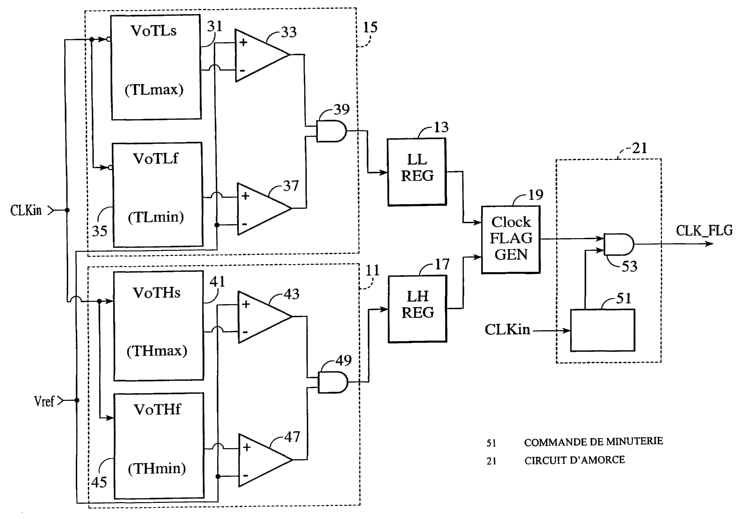
With reference to Fig. 4, a block diagram of a
circuit suitable for implementing the present invention
is shown. A logic low monitor block 15 monitors received
logic low pulses and a logic high monitor block 11
monitors received logic high pulses. Both logic low and
logic high monitor blocks 15 and 11 preferably receive
the same reference signal Vref, and both receive a pulse
signal, exemplified by received clock signal CLKin.
Each of logic high and logic low monitor blocks
11 and 15 include within themselves a pair of linear
voltage ramps and a means for comparing their respective
linear voltage ramps with reference signal Vref. For
example, logic low monitor block 15 includes a first
slower linear voltage ramp generator producing an output
VoTLs similar to that shown in Fig. 2, and include a
second faster voltage ramp generator producing an output
VoTLf also similar to that of Fig. 2. Its first and
second linear voltage ramp generators are reset and begin
ramping up upon receiving a logic low pulse. Their
respective outputs VoTLs and VoTLf continue to ramp up
while the received pulse is at a logic low. When the
received signal CLKin transitions to a logic high, the
values of VoTLf and VoTLs are compared with reference
signal Vref. If at the time that CLKin transitioned to a
logic high, VoTLf was at a higher potential than Vref and
VoTLs was at a lower potential than Vref, then CLKin
transitioned within the desired transition window W0.
Logic low monitor block 15 will therefore send a "good
pulse cycle" signal to a logic low register 13. If, on
the other hand, signal VoTLf was not higher than Vref or
signal VoTLs not lower than Vref at the time that CLKin
transitioned to a logic high, then the logic pulse was
ether too short or too long and a "bad pulse cycle"
signal would have been sent to logic low register 13.
Logic low register 13 stores the result from logic low
CA 02388662 2002-04-15
WO 01/37427 PCT/US00/41227
-10-
monitor block 15 until the next logic low pulse cycle and
provide the result to a flag generator 19.
Similarly, logic high monitor block 11 includes
within itself a third slower linear voltage ramp
producing an output VoTHs similar to that shown in Fig. 3
and a fourth faster linear voltage ramp producing an
output VoTHf similar to that of Fig. 3. Logic high
monitor block 11 also includes a means for comparing
VoTHs and VoTHf with reference voltage Vref. When input
signal CLKin produces a logic high pulse, third and
fourth linear voltage ramps are reset and begin producing
respective outputs VoTHs and VoTHf while signal CLKin
remains at a logic high. When input CLKin transistions
back to a logic low, the values of VoTHf and VoTHs are
compared with reference voltage Vref. If at the time
that CLKin transitioned to a logic low, VoTHf was at a
higher potential than Vref and VoTHs was at a lower
potential than Vref, then CLKin transitioned within W1
and a "good pulse cycle" signal is sent to logic high
register 17. By contrast, if VoTHf was not higher than
Vref or VoTHs was not lower than Vref at the time that
CLKin transitioned to a logic low, then the transition
was either too long or too short and did not take place
within W1. In this case, a "bad pulse cycle" signal
would be issued to logic high register 17. Logic high
register 17 stores the result of logic high monitor 11
until the next logic high pulse cycle and provides the
stored results to flag generator 13.
A clock flag generator 19 compares the result
of the most current pulse cycle with that of the previous
pulse cycle. If both the current pulse cycle and the
previous pulse cycle received a "good pulse cycle"
single, then flag generator 19 produces an enable signal.
If the current pulse cycle received a "bad pulse cycle"
signal, then flag generator 19 will issue a disable
signal irrespective of the condition of the previous
CA 02388662 2002-04-15
WO 01/37427 PCT/US00/41227
-11-
clock cycle. If the current pulse cycle received a "good
pulse cycle" signal, but the previous pulse cycle
received a "bad pulse cycle" signal, then a flag
generator 19 will produce a disable signal. The enable
and disable signals produced by flag generator 19 may be
directly applied to other circuits responsive to the
present pulse monitoring circuit, or it may be gated by
an initiation circuit 21.
Initiation circuit 21 includes a timing means
and can selectively transfer the output of flag generator
19 to output signal CLK FLG for application to other
circuits responsive to the present pulse monitoring
circuit, or apply a disable signal to output signal
CLK FLG.
Initiation circuit 21 is preferably reserved
for start-up conditions. During start-up, the present
pulse monitoring circuit and the other circuits
responsive to the present pulse monitoring circuit may
require a setup period to achieve stable start-up
conditions. Initiation circuit 21 therefore provides a
wait period at startup to give other circuitry time to
reach their stable start-up conditions. During start-up,
initiation circuit 21 initiate a wait period by
transferring a disable signal onto output lead CLK-FLG
for a predetermined amount of time or a predetermined
amount of CLKin cycles. At the end of the wait period,
initiation circuit 21 then permits the output of flag
generator 19 to be freely transferred onto output lead
CLK FLG.
With reference to Fig. 5, a graphical example
of the interaction of logic high monitor block 11, logic
low monitor block 15, reference signal Vref, output of
clock flag generator 19, and input pulse signal CLKin is
shown. Input signal CLKin is shown to consist of seven
logic high and logic low pulses of differing pulse
lengths. The interaction of reference signal Vref along
CA 02388662 2002-04-15
WO 01/37427 PCT/US00/41227
-12-
with monitor blocks 11 and 15 determine if the pulse
lengths of CLKin fall within the predetermined transition
windows WO and W1. Preferred transitions windows WO and
W1 are shown as shaded areas, and numerical values 0 and
1 symbolically denote the result of the means included
within each of monitor blocks 11 and 15 for comparing
their respective linear voltage ramps with reference
voltage Vref.
In Fig. 5, logic high monitor block 11 is shown
to use a faster linear voltage ramp 35 and a slower
linear voltage ramp 31 to observe logic high pulses P1,
P3, P5, and P7 of signal CLKin. As shown, respective
linear voltage ramps 31 and 35 begin ramping up upon
reception of a logic high pulse of CLKin. The values of
linear voltage ramps 31 and 35 are shown continuously
compared with reference signal Vref, but it is not
critical that linear voltage ramps 31 and 35 be
continuously compared with reference signal Vref. It is
sufficient that at least the values of linear voltage
ramps 31 and 35 at the time that a CLKin logic high pulse
ends be compared with reference signal Vref. In the
present example, the numbers 0 and 1 above linear voltage
ramp 35 correspond to the comparison results of faster
linear voltage ramp 35 with reference voltage Vref. A
value of 0 indicates that linear voltage ramp 35 is below
Vref and a value of 1 indicates that linear voltage ramp
is above Vref. Also in the present example, numbers 0
and 1 below slower linear voltage ramp 31 indicate the
result of the comparison results of slower linear voltage
30 ramp 31 with reference voltage Vref. A value of 1
indicates that linear voltage ramp 31 is below Vref and a
value of 0 indicates that it is above Vref.
Similarly, logic low monitor block 15 is shown
to use a faster linear voltage ramp 45 and a slower
35 linear voltage ramp 41 to observe logic low pulses P2,
P4, and P6 of signal CLKin. Respective linear voltage
CA 02388662 2002-04-15
WO 01/37427 PCT/US00/41227
-13-
ramps 41 and 45 begin ramping up upon reception of a
logic low pulse of CLKin. In the present example, linear
voltage ramps 41 and 45 are continuously compared with
reference signal Vref, but if desired they can be
compared with Vref only at the end of a logic low pulse.
Like in the previous case, numbers 0 and 1 above linear
voltage ramp 45 correspond to the comparison results of
faster linear voltage ramp 45 with reference voltage
Vref, and numbers 0 and 1 below linear voltage ramp 41
indicate the result of the comparison results of slower
linear voltage ramp 41 with reference voltage Vref. As
applied to faster linear voltage ramp 45, a comparison
value of 0 indicates that it is below Vref and a
comparison value of 1 indicates that it is above Vref.
In regards to slower linear voltage ramp 41, however, a
value of 1 indicates that it is below Vref and a value of
0 indicates that it is above Vref.
Voltage ramps 31, 35, 41 and 45 are shown to be
reset at the end of the respective logic high or logic
low CKLin pulse that they are observing, but this is not
critical to the invention. Voltage ramps 31, 35, 41 and
45 may continue ramping pass the end of the respective
logic high or logic low pulse they are observing. They
should, however, be reset by the beginning of a new
respective logic high or logic low pulse.
With reference to pulses P1 to P7, faster
linear voltage ramps 35 and 45 maintain a comparison
value of 0 while ramping up until they reach the lower
boundary of their respective preferred transition window,
indicated by a shaded area. This lower boundary is
marked by their respective crossing over reference signal
Vref. Faster linear voltage ramps 35 and 45 then
maintain a comparison value of 1 once they have achieved
values greater than Vref. By contrast, slower linear
voltage ramps 31 and 41 maintain a comparison value of 1
while ramping up until they reach the upper boundary of
CA 02388662 2002-04-15
WO 01/37427 PCT/US00/41227
-14-
their respective preferred transition window, indicated
by the shaded area. This upper boundary is marked by
their respective crossing over reference signal Vref.
Slower linear voltage ramps 31 and 41 then maintain a
comparison value of 0 once they reach values greater than
Vref. The choice of whether a value of 1 indicated that
a linear voltage ramp is above or below Vref is
arbitrary. In the present example, a comparison value of
1 is used with faster linear voltage ramps 35 and 45 to
indicate that they are above Vref, while a comparison
value of 1 is used with slower linear voltage ramps 31
and 41 to indicate that they are below Vref. This
arbitrary choice was made so that the preferred
transition regions of monitor blocks 11 and 15 would be
denoted by their respective faster and slower linear
voltage blocks both having a comparison value of 1
simultaneously.
With reference to logic high pulse P1, logic
high monitor block 11 shows that Pl ended while both
slower linear voltage ramp 31 and faster linear voltage
ramp 35 had a comparison value of 1. Therefore, P1
transitioned within its preferred transition window and
it receives a pulse status of G, indicated a "good pulse
cycle". Flag generator 19 receives this result and
compares it with the previous cycle. In the present
example, it is assumed that the previous cycle was also a
good pulse cycle and flag generator 19 therefore outputs
an enable signal EN.
Logic low monitor block 15 tracks logic low
pulse P2. Pulse P2 is shown to end while faster linear
voltage ramp 45 and slower linear voltage ramp 41 both
have a comparison value of 1. This indicates that P2
terminated within its preferred transition window and
therefore also receives a status of G, indicating a "good
pulse cycle". Flag generator 19 receives this G status
and compares it with the status of previous pulse P1.
CA 02388662 2002-04-15
WO 01/37427 PCT/US00/41227
-15-
Since both current pulse P2 and previous pulse P1 have a
G status, flag generator again issues an enable signal
EN.
Logic high pulse P3 is shown to end while
slower linear voltage ramp 31 has a comparison value of
1, but faster linear voltage ramp 35 has a comparison
value of 0. P3 therefore terminated before it reached
its preferred transition region. Logic high monitor
block 11 therefore categorizes it as a "bad pulse cycle"
and gives it a status B. Upon receiving the status B
result from monitor block 11, flag generator 19 issues a
disable signal DIS.
Logic low monitor block 15 then observes the
next pulse, P4. By the time pulse P4 ends, slower linear
voltage ramp 41 has already risen above Vref and obtained
a comparison value of 0. Since slower linear voltage 41
and faster linear voltage ramp 45 do not both have a
comparison value of 1 when P4 ends, logic low monitor
block 15 determines that P4 did not terminate within it s
preferred transition window and gives it a B status
indicating a "bad pulse cycle". Upon receiving the status
B result from monitor block 15, flag generator 19 issues
a disable signal DIS.
Logic high pulse P5 is shown to transition
within its preferred transition region, as determined by
linear voltage ramps 35 and 31. Logic high monitor block
11 therefore categorizes its as a "good pulse cycle" and
gives it a good status, G. Flag generator 19 receives
this G status and compares it with the status of the
immediately previous pulse, P4. Since P4 had a bad, B,
status, flag generator 19 issues a disable signal DIS on
its output in spite of the current pulse, P5, being a
good pulse. This is because in the currently preferred
embodiment, flag generator 19 does not issue an enable
signal until it receives two consecutive good CKLin
pulses.
CA 02388662 2002-04-15
WO 01/37427 PCT/US00/41227
-16-
As shown, logic low pulse P6 also receives a
good status, G, by logic low monitor block 15. Again,
this is because P6 transitioned within its preferred
transition region denoted by the shaded area. Flag
generator 19 receives the G status from pulse P6 and
compares it with the status of the immediately previous
pulse, P5. Since both the current P6 pulse and previous
P5 pulse both have a G status, flag generator 19 issues
an enable signal EN on its output. The same is case for
pulse P7, which receives a G status from logic high
monitor block 11 for transition during a time when both
linear voltage ramps 35 and 31 have a comparison value of
1. Flag generator 19 compares pulse P7 with pulse P6,
and since both have a G status, flag generator 19
maintains its enable signal EN on its output.
With reference to Fig. 6, a first circuit
implementation of the block diagram of Fig. 4 is shown.
All elements in Fig. 6 similar to those of Fig. 4 are
identified with similar reference characters and are
described above. It is to be understood that there are
many implementations for the functional block diagram of
Fig. 4, and that the structure shown in Fig. 6 a
currently preferred embodiment and does not limit the
present invention. If desired, for example, the linear
voltage ramps within monitor blocks 11 could be
represented by a digital counter and the functional block
diagram of Fig. 4 implemented in software, in a
programmable logic device, FPGA, or other rendering
method known in the art.
Logic high monitoring block 11 includes a
faster linear voltage ramp generator 35 and a slower
linear voltage ramp generator 31. The output voltage
ramp from slower voltage ramp generator 31 has a lower
slope than the output from faster linear voltage ramp
generator 35. Both linear voltage ramp generators 31 and
35 are preferably active high devices and respond to a
CA 02388662 2002-04-15
WO 01/37427 PCT/US00/41227
-17-
logic high pulse on input signal CLKin by initiating
their respective output voltage ramps. The output from
linear voltage ramp 31 is applied to the inverting input
a first differential amplifier 33. The non-inverting
input of differential amplifier 33 receives input
reference voltage Vref. Differential amplifier 33 will
therefore maintain a logic high output until the output
from slower linear voltage ramp 31 rises above Vref. At
that point the output from differential amplifier 33 will
switch to a logic low. By contrast, the output of faster
linear voltage ramp generator 35 is applied to the non-
inverting input of a second differential amplifier 37,
and Vref is applied to the inverting input of
differential amplifier 37. The output of differential
amplifier 37 will therefore remain at a logic low until
the output from faster linear voltage ramp 35 rises above
Vref. At that point, the output from differential
amplifier 37 will switch to a logic high. As explained
above, the preferred transition region is denoted by the
time period during which the output from slower linear
voltage ramp 31 is below Vref and the output from faster
linear voltage ramp is above Vref. Under these
conditions, the output from first differential amplifier
33 and second differential amplifier 37 both have a logic
high output simultaneously. An AND gate 39 issues a
logic high when both differential amplifiers 33 and 37
have an logic high output, indicating that the observed
pulse is within it preferred transition region.
The structure of logic low monitor block 15 is
similar to that of monitor block 11 with only minor
changes. In case of logic low monitor block 15, a slower
linear voltage ramp generator 41 and a faster linear
voltage ramp generator 45 are active low devices and
respond to a logic low pulse at input CLKin. When CLKin
switches to a logic low pulse, both the faster and slower
linear voltage ramp generators 41 and 45 respond by
CA 02388662 2002-04-15
WO 01/37427 PCT/US00/41227
-18-
producing their respective output voltage ramps. The
output slow of the slower voltage ramp generator 45 is
lower than the slow of the faster linear voltage ramp
generator 41. The output of slower voltage ramp
generator 41 is applied to the inverting input of a third
differential amplifier 43, and input reference voltage
Vref is applied to the non-inverting input of
differential amplifier 43. The differential amplifier 43
will issue a logic high until the output from slower
linear voltage ramp 41 rises above Vref. On the other
hand, the output from faster linear voltage ramp 45 is
applied to the non-inverting input of a fourth
differential amplifier 47 and Vref is applied to its
inverting input. Differential amplifier 47 will
therefore issue a logic low until the output from faster
linear voltage ramp generator 41 rises above Vref. The
preferred transition window is define by the time period
during which both differential amplifiers 43 and 47
simultaneously have a logic high output. A second AND
gate 49 determines when both differential amplifiers 43
and 47 have a logic high output.
The resultant output from AND gates 39 and 49
are preferably sent to respective memory devices 13 and
17, implemented as registers in the presently preferred
embodiment. If it is not necessary that the current
pulse be compared with the previous pulse, however, then
memory devices 13 and 17 are not necessary. Flag
generator 19 receives the output from logic low register
memory 13 and from logic high register memory 17, and
compares the current pulse results with the previous
pulse results. Flag generator 19 preferably issues an
enable signal EN in response to CLKin having two
consecutive pulses that transitioned within their
respective preferred transition region.
The output from flag generator 19 is preferably
applied to an initiation circuit 21, which masks out
CA 02388662 2002-04-15
WO 01/37427 PCT/US00/41227
-19-
output from flag generator 19 during a start-up period
and replaces it with a disable signal DIS. In the
present embodiment, a logic high on output signal CLK-FLG
represents an enable signal EN and logic low on CLK_FLG
represents disable signal DIS. An AND gate 53
selectively masks the output from Flag generator 19 for a
predetermined amount of time or a predetermined number of
pulses on signal CLKin. A time control circuit 51
determines when to mask the output from flag generator
19.
Fig. 7 offers a more detailed circuit level
implementation of the structures of Figs. 4 and 6. All
elements similar to those of Figs. 4 and 6 have similar
reference characters and are described above. Faster and
slower linear voltage ramp generators 31 and 35 may have
a similar implementation. For example, each has a
respective constant current source 61 and 67 that can
selectively charge a respective capacitive means 63 and
68. The output of each linear voltage ramp generator is
taken at respective junctions 66 and 68 joining their
respective constant current sources and capacitive means.
The slop of a an output voltage ramp at either of
junctions 66 or 68 is determined by the strength of their
respective current source 61/67 and the capacitance of
their respective capacitive means 63/68. Assuming that
the capacitance of capacitive means 63 and 69, the ramp
rate of nodes 66 and 68 may be adjusted by altering the
strength of respective constant current sources 61 and
67. In the present example, the strength of constant
current sources 61 and 67 is controlled by respective
control signals C1 and C2. Thus, one can adjust the
difference in ramp rate at nodes 66 and 68, and thereby
adjust W0, by adjusting control lines Cl and C2. This
offers another degree of freedom since one can now adjust
the size of the preferred transition window either by
changing Vref or by changing C1 and C2.
CA 02388662 2002-04-15
WO 01/37427 PCT/US00/41227
-20-
A fist switch 65 can selectively reset the
voltage potential at node 66. Similarly, a second switch
71 can selectively reset the voltage potential at node
68. Since linear voltage ramps 31 and 35 are intended to
respond to a logic low pulse at CLKin, switches 65 and 66
are shown as active low devices responsive to a logic low
input.
Linear voltage ramps 41 and 45 of logic high
monitor block 11 are shown to have substantially the same
structure as linear voltage ramps 31 and 35 of logic low
monitor block 15. The basic differences is that linear
voltage ramps 41 and 45 are shown responsive to a second
pair of respective current control signals C3 and C4, and
switches 85 and 91 are shown as active high devices.
Therefore, switches 85 and 91 would respond to a logic
high at CLKin and permit monitor block 11 to track
positive pulses at CLKin.
Memory registers 13 and 17 are shown
implemented as D flip-flops clocked by CKLin. This
permits them to latch the result of their respective AND
gate input, 36 and 49, at the point when CLKin
transitions. For example, If logic low monitor block 15
is tracking a logic low pulse at CLKin, the output from
AND gate 39 will change with time from a logic low to a
logic high as the length of the logic low CLKin pulse
enters its preferred transition region. If the length of
the logic low CLKin pulse persists pass its preferred
transition region, then AND gate 39 would again changed
from a logic high to a logic low. Having logic low
register 13 clocked on the logic low to logic high pulse
transition of CLKin allows register 13 to latch the
current state of AND gate 39. Similarly, logic high
register 17 is clocked on the logic low transition of
CLKin in order to latch in the state of AND gate 49 when
a monitored logic high CLKin pulse transitions to a logic
low.
CA 02388662 2002-04-15
WO 01/37427 PCT/US00/41227
-21-
Thus, one of memory registers 13 and 17 will
also have the status of a current CLKin pulse and the
other will have the status of the previous CLKin pulse.
Since a good status G is represented by a logic high and
bad status B is represented by a logic low, a current
good CLKin pulse following a previous good CLKin pulse is
represented when both memory registers 13 and 17 have a
logic high at their respective outputs. Flag generator
19 is represented by an AND gate 73 and will issue a
logic high enable signal EN only when both memory
registers 13 and 17 have logic high output, and will
issue a logic low disable signal DIS otherwise.