Note: Descriptions are shown in the official language in which they were submitted.
CA 02388872 2002-04-22
WO 02/23259 PCT/USO1/28549
1
REVERSIBLE ELECTROCHEMICAL MIRROR (REM) STATE MONITORING
BACKGROUND OF THE INVENTION
Field of the Invention
This invention is concerned with devices, such as mirrors and windows, having
controllable reflectivity.
Description of fhe Related Art
Sunlight transmitted through windows in buildings and transportation vehicles
can
generate heat (via the greenhouse effect) that creates an uncomfortable
environment and
increases air conditioning requirements and costs. Current approaches to
providing "smart
windows" with adjustable transmission for use in various sunlight conditions
involve the use of
light absorbing materials. These approaches are only partially effective,
since the window itself
is heated and because these devices, such as electrochromic devices, are
relatively expensive and
exhibit limited durability and cycle life. Certain liquid crystal-based window
systems switch
between transmissive and opaque/scattering states, but these systems require
substantial voltages
to maintain the transparent state. There is an important need for an
inexpensive, durable low
voltage smart window with variable reflectivity. Reflecting the light, rather
than absorbing it,
is the most efficient means for avoiding inside heating. Devices for
effectively controlling
transmission of light are also needed for a variety of other applications,
e.g., energy efficient
dimmers for displays.
Bright light from headlamps on following vehicles reflected in automobile rear
and side
view mirrors is annoying to drivers and creates a safety hazard by impairing
driver vision.
Currently available automatically dimming mirrors rely on electrochromic
reactions to produce
electrolyte species that absorb light that would otherwise be reflected from a
static mirror. Such
devices do not provide close control over the amount of reflected light, and
are expensive to
fabricate since a very constant inter-electrode spacing is required to provide
uniform dimming.
Image sharpness is also reduced for electrochromic mirror devices since the
reflected light must
pass through the electrolyte (twice). There is an important need for an
inexpensive adjustable
mirror device that provides close control of reflected light with minimal
image distortion.
In early attempts to exploit reversible electrodeposition of a metal for light
modulation,
the deposits obtained on transparent substrates presented a rough and black,
gray, or sometimes
colored appearance (typical of finely-divided metals) and exhibited poor
reflectivity and high
CA 02388872 2002-04-22
WO 02/23259 PCT/USO1/28549
2
light absorbance; especially when thick. Such deposits have been investigated
for display
applications involving reflectance from the background, with white pigments
often being added
to improve contrast. Warszawski (U.S. Patent No. S,OS6,899), which is
concerned with displays,
teaches that reversible metal electrodeposition is most appropriate for
display applications, since
S significant disadvantages for transmission devices were given (e.g., the
possibility of metal
deposition at the counter electrode). In general, the prior art literature
teaches that an auxiliary
counter electrode reaction is required for transmission-type devices to avoid
metal
electrodeposition at the counter electrode as metal electrodissolution occurs
at the working
electrode, which would produce no net change in transmission. Such teachings
imply that the
application of reversible metal deposition to smart windows must involve light
absorption by the
finely divided electrodeposited metal, which would result in heating of the
device itself and thus
the space inside. The low reflectance of this type of deposit would not be
appropriate for
adjustable mirror applications.
Electrolytes described in the early prior art literature contain auxiliary
redox species (e.g.,
1 S bromide, iodide, or chloride) that ,are oxidized (e.g., to bromine,
iodine, or chlorine) at the
counter electrode during metal deposition under the high drive voltages used.
This introduces
chemistry-related instabilities during long term operation and leads to
deposit self erasure on
open circuit via chemical dissolution of the metal deposit, e.g., 2Ag°
+ Br, ---> 2AgBr. In most
cases, this auxiliary redox process hinders metal deposition at the' counter
electrode during
erasure, introducing a threshold voltage that is desirable for display
applications. This auxiliary
redox process may represent a significant side reaction even when metal
electrodeposition/dissolution occurs at the counter electrode and a threshold
voltage is not
observed. See, e.g., Warszawski, columns 3-4 (when copper or nickel were
present in the
counter electrode paste) and Duchene et al., Electrolytic Display, IEEE
Transactions on Electron
2S Devices; Volume ED-26, Number 8, Pages 1243-1245 (August 1979); French
Patent No.
2,504,290 (October 22, 1982). High switching voltages of at least 1 V were
used for all the
electrodeposition devices which have been found in.the patent and literature
prior art.
A paper by Ziegler et al. (Electrochem. Soc. Proc. Vol. 93-26, p. 353, 1993)
describes an
investigation for display applications of the reversible electrodeposition of
bismuth in aqueous
solutions containing a large molar concentration ratio of halide anions to the
trivalent bismuth
ion. Halide anion oxidation served as the counter electrode reaction with the
1.S V write voltage
used. The deposits obtained were dark in color and were shown to decrease the
reflectance of
CA 02388872 2002-04-22
WO 02/23259 PCT/USO1/28549
3
the ITO surface. Subsequent reports by these authors (Electrochem. Soc. Proc.
Vol. 94-31
(1994), p. 23; Solar Energy Mater. Solar Cells 39 (1995), p. 317) indicated
that addition of
copper ions to the electrolyte was necessary to attain complete deposit
erasure. These authors also
utilized a counter electrode reaction other than metal
electrodeposition/dissolution, and also
never obtained a mirror deposit. Thus, Ziegler et al. provide no teachings
relevant to the effect
of electrolyte composition on the deposition/dissolution rate and quality of
mirror
electrodeposits.
Warszawski teaches that the use of a grid counter electrode would give a less
uniform
deposit since deposition on the transparent working electrode is highly
localized in the vicinity
of the counter electrode grid lines (a consequence of the very thin film of
gel electrolyte used).
Warszawski also teaches the use of an aqueous gel electrolyte to minimize
sensitivity to
atmospheric contaminants and to avoid the necessity of having a leak tight
seal. Such
electrolytes, however, have much more limited temperature and voltage
operating ranges
compared with organic-based electrolytes with high boiling solvents.
One effort to improve the deposit quality of the electrolytic solution used in
a reversible
electrodeposition process, described in U.S. Patent No. 5,764,401 to Udaka et
al., requires the
addition of organic additives to the solution. Unfortunately, such additives
are typically destroyed
during the electrodeposition process, greatly limiting cycle life.
Furthermore, this approach fails
to produce highly-reflective mirror-Like deposits that are required for
adjustable mirror
applications and provide the superior heat rejection needed for smart windows.
U.S. Patent 5,880,872 to Udaka teaches that the "working" electrode of a
reversible
electrodeposition structure is degraded, and its working life thereby
shortened, by the high
voltage required to dissolve the metal film deposited upon it. Udaka states
that this consequence
can be avoided by adding an alkali metal halide to the device's electrolytic
solution, preferably
in an amount which provides an alkali metal halide to silver halide ratio of
between 0.5 to 5.
However, the described electrolytic formulation fails to provide the inherent
stability, high
quality deposits, good erasure and long cycle life needed for practical
applications. Mirror
deposits were never obtained.
Prior art literature teaches that the memory effect is temporary. This is a
consequence of
the occurrence of a counter electrode reaction other than metal
electrodeposition/dissolution. The
energetic oxidation products generated at the counter electrode can cause
dissolution of the metal
deposit on the working electrode either chemically on open circuit (slow) or
electrochemically
CA 02388872 2002-04-22
WO 02/23259 PCT/USO1/28549
4
during short circuit (fast).
Nishikitani. et a1._ (European Patent No. 0,618,477) teaches that the counter
electrode in. _ _
electrochromic devices for smart window applications can be a metal grid which
is substantially
transparent. Since no metal electrodeposition occurs in electrochromic
devices, however, the
grid in this case is used to provide a transparent electrode, not to maintain
transparency by
localizing metal deposition. In addition, to provide adequate electrical
capacity for
electrochromic devices, Nishikitani's grid would need a very high surface area
(at least 10 m2/g
and preferably 50 to 5,000 m2/g) and a line width of 50 to 5,000 qm;
alternatively, a plurality of
dots on a conducting substrate can be used, but the dots must contain fine
particles having
electrical capacitance of not less than 1 farad/g.
A reversible electrochemical mirror (REM) device permitting efficient and
precise control
over the reflectioutransmission of visible light and other electromagnetic
radiation is described
in U.S. Patents 5,903,32 and 5,923,456 to Tench et al., which are assigned to
the same assignee
as the present application. In this device, an electrolyte containing ions of
an electrodepositable
metal is sandwiched between a mirror electrode and a counter electrode, at
least one of which is
substantially transparent to the radiation. A typical transparent mirror
electrode is indium tin
oxide (ITO) or fluorine doped tin oxide (FTO) deposited on a transparent glass
(or plastic) pane
which serves as the substrate. Application of a voltage causes the
electrodepositable metal, e.g.,
silver, to be deposited as a mirror on the mirror electrode while an equal
amount of the same
metal is dissolved from the counter electrode. When the voltage polarity is
switched, the overall
process is reversed so that the mirror metal is at least partially dissolved
from the mirror
electrode. A thin layer of noble metal, e.g., 15 - 30A platinum, on the
transparent conductor is
usually required to improve nucleation so that a mirror deposit is obtained.
The thickness of
mirror metal layer present on the mirror electrode determines the reflectance
of the device for
radiation, which can be varied over a wide range.
The REM technology can be used to provide control of either light reflectance,
transmission, or both. A transmissive REM device suitable, for smart window
applications
utilizes a noble metal counter electrode that is locally distributed, e.g., in
a grid, on a transparent
substrate, e.g., glass, so that mirror metal deposited thereon does not
appreciably increase light
blockage. In this case, high light transmission is provided by a locally
distributed counter
electrode of relatively small cross-sectional area and the device
reflectance/transmission is
adjusted via the thickness of mirror metal on the mirror electrode. As
described in U.S. Patent
CA 02388872 2002-12-20
WO 02/23259 PCTIUSOI/285.~9
s
to Tench et al., such a transinissive counter electrode is not required for
reflective REM
devices used for adjustable minor applications. An electrolytic solution
providing the inherent
stability, high deposit quality, complete deposit erasure, long cycle life and
fast switching needed
for most practical applications is described in U.S. Patent 6,111,685, issued
August 29, 2000,
which is assigned to the same assignee as the present invention.
A significant problem with adjustable mirrors of the type suitable for
automotive
applications, including both REM and electrochromic mirrors, is that simple
means for
monitoring the reflectance of such devices are not available. Consequently, it
is necessary to
place a light sensor in front of the mirror to provide feedback so that the
reflectance can be
adjusted to the desired level. Such sensors are not only expensive but are
also aesthetically
undesirable, increase the bulkiness of the device, and typically monitor only
a small area while
blocking a portion of the mirror itself. Similar difficulties exist for
variable transmission devices
as well. An inherent means for monitoring the mirmr state of adjustable
reflectance/transmission
devices could provide significant advantages in terms ofcosts, performance,
space utilization and
I S market acceptance.
SUMMARY OF THE IN~JENTION
This invention involves use of a relatively simple electrical measurement to
determine
the state of the mirror electrode in a reversible electrochemical mirror (REM)
device, which is
comprised of an electrolyte containing electrodepositable metal ions, e.g.,
silver ions, in contact
with a mirror electrode and a counter electrode. The electrolyte may be a
solid electrolyte, a
liquid electrolytic solution, or an electrolytic solution rendered viscous,
semi-solid or solid via
a stiffening agent. The mirror electrode is typically comprised of a thin
layer of noble metal (e.g.,
platinum) on a layer of a transparent conducting oxide (e.g., indium tin
oxide) on a glass or
plastic substrate. Generally, the counter electrode is a sheet or layer of the
electrodepositable
mirror metal for devices that are designed to control radiation reflection,
and is a locally
distributed electrode for devices that also transmit radiation. The device
reflectance is determined'
by the thickness of the mirror metal layer on the mirror electrode, which can
be adjusted by
applying a voltage of the appropriate polarity to cause mirror metal
eiectrodeposition or
dissolution, while the reverse process occurs at the counter electrode.
According to the method of the present invention, the thi ckness of mirror
metal deposited
on the minor electrode of a reversible electrochemical mirror (REM) is
determined from its
CA 02388872 2002-04-22
WO 02/23259 PCT/USO1/28549
6
effect on the sheet resistance of the mirror electrode, which provides an
indirect measure of the
reflectance of the device. A thin layer of deposited mirror metal has a large
effect on the sheet
resistance since the resistivity of the transparent oxide conductor typically
used for~the mirror
electrode is relatively high (at least 10 ohmlsquare). Note that the parallel
current path through
the electrolyte has a negligible effect for the relatively resistive
electrolytes and small cell gaps
typically employed. The resistance is measured between two separate contacts
placed on the
REM mirror electrode, which may be the same ones used to apply voltage for
switching the
mirror state of the device. One preferred configuration for a rectangular
mirror electrode is to
place the electrical contacts only along two opposite sides so that the
measured resistance reflects
the average thickness of deposited mirror metal. This configuration also
yields the most uniform
mirror formation and erasure, and consequently the most uniform mirror
reflectance. Direct
contact between the electrical contacts and the electrolyte should be avoided
since plating on the
contacts could affect the uniformity of the mirror deposits obtained. For the
preferred
configuration of rectangular mirrors given above, the mirror uniformity and
measurement
precision can be further improved by minimizing the extent to which the sides
of the mirror
electrode not provided with electrical contacts extend beyond the mirror
border, e.g., into a seal..
Resistance between the two electrical contacts may be determined from the
current
response to a direct (dc) or alternating (ac) voltage applied across the two
separate contacts on
the mirror electrode. An ac voltage is usually advantageous to minimize
voltage losses due to
contact resistances between the contacts and the mirror electrode, which may
vary appreciably
with time and would introduce errors in the measurement. The voltage
perturbation frequency
is preferably chosen to minimize contact resistances as well as the effects of
capacitive and
inductive losses, which introduce a phase shift between the applied ac voltage
and the ac current
response. In some cases, it may be necessary to take this phase shift into
account to calculate an
accurate sheet resistance for the mirror electrode.
By utilizing appropriate circuitry and contact configurations, the sheet
resistance of the
mirror electrode can be determined while mirror metal is being deposited or
erased so as to
permit the thickness of deposited mirror metal, and indirectly the device
reflectance, to be
monitored during mirror state switching. One simple approach is to use the
same contacts for
switching the mirror state and measuring its sheet resistance and to place
equivalent resistors
between each ofthe two mirror electrode contacts and the switching voltage
source. Such parallel
resistors reduce the overall resistance between the contacts but can be chosen
to be sufficiently
CA 02388872 2002-04-22
WO 02/23259 PCT/USO1/28549
7
large that good sensitivity to the thickness of mirror metal is retained. In
this case, an ac rather
than a do resistance measurement is preferred to minimize mutual interference
between the
mirror state switching and measurement processes. For this approach,
additional switching
voltage is required to offset the voltage drops across the isolation
resistors, which are in series
with the switching power source. More sophisticated circuitry could be used to
avoid significant
resistance in the switching circuit and to more effectively isolate it from
the measurement circuit.
A preferred approach is to provide separate contacts for mirror state
switching and the sheet
resistance measurement and utilize the mirror electrode sheet resistance
itself to provide adequate
circuit isolation.
Further features and advantages of the invention will be apparent to those
skilled in the
art from the following detailed description, taken together with the
accompanying drawings.
BRIEF DESCRIPTION OF THE DRAWINGS
Figure 1 is a cross sectional view depicting a representative design of a
reversible
electrochemical mirror (REM) device.
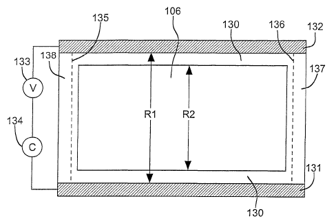
Figure 2 is a schematic representation of a mirror electrode of a reversible
electrochemical mirror (REM) device (as viewed from the electrolyte side)
illustrating a suitable
contact arrangement and measurement system for determining the thickness of
mirror metal
deposited on the mirror electrode.
Figure 3 is a cross sectional view similar to Figure 1, but also showing the
contact-seal
arrangement of Figure 2 and illustrating the use of external resistors to
provide partial electrical
isolation for mirror electrode sheet resistance measurements during mirror
state switching with
the same electrical contacts.
Figure 4 is a schematic representation similar to Figure 2 but illustrating
placement of
separate electrical contacts to provide electrical isolation for mirror
electrode sheet resistance
measurements during mirror state switching.
Figure 5 gives a plot of the resistance measured between buss bars attached
outside the
seal area of a REM device (containing a silver halide electrolyte) as a
function of the silver
thickness on the mirror electrode.
Figure 6 gives a plot of reflectance at 700 nm wavelength as a function of
measured sheet
resistance for the same REM device as for Figure S.
CA 02388872 2002-04-22
WO 02/23259 PCT/USO1/28549
8
DETAILED DESCRIPTION OF THE INVENTION
Figure 1_ is a cross sectio,~al~ view depicting a representative design. of a
reversible
electrochemical mirror (REM) to which the present invention pertains. Some
dimensions,
particularly layer thicknesses, are disproportionate in the drawings in order
to more effectively
illustrate the structure and function of the device. The REM device in this
example, which
provides precise control over the reflection of electromagnetic radiation,
includes a first substrate
102, which is substantially transparent to the portion of the spectrzun of
electromagnetic radiation
which is to be controlled, and a second substrate 104. An electrically
conducting film 106, which
is also substantially transparent, is deposited on the first substrate. The
film 106, with the
optional addition of an electrochemically stable surface modification layer
108, functions as the
mirror electrode. The conducting oxide film 106 is typically indium tin oxide
(ITO) or fluorine
doped tin oxide (FTO). The surface modification layer 108 is typically a noble
metal selected
from the group consisting of platinum, iridium, gold, osmium, palladium,
rhenium, rhodium and
ruthenium. An underlayer of another metal (e.g., aluminum, chromium, hafnium,
molybdenum,
nickel, titanium, tungsten or zirconium) may be used to improve the adhesion
of surface
modification layer 108.
A second electrode 110 is deposited on the second substrate 104 and functions
as the
counter electrode. The counter electrode 110 can alternatively be a bulk
electrode, a metal plate
or sheet for example, with sufficient rigidity that the second substrate 104
would not be needed.
For a device that also transmits radiation, electrode 110 may be a locally
distributed electrode
(not shown in Figure 1), as described in U.S. Patent 5,923,456 to Tench et
al., which is assigned
to the same assignee as the present application. The counter electrode 110 is
electrochemically
stable or is covered with a sufficient thickness of an active metal layer 114
to avoid exposure of
the counter electrode surface to the electrolyte. It may also be protected
from exposure to the
electrolyte by a coating of electrochemically'stable metal. Relatively stable
metals that might be
used as the counter electrode material or as a protective layer or coating on
the counter electrode
include Pt, Ir, Au, Os, Pd, Re, Rh, Ru, Cr, Ni, Ti and stainless steel. The
surface of electrode
110 may be roughened to reduce reflection of radiation from the electrode or
to improve
switching speed by lowering the current density (via increased surface area).
An electrolyte 112 is located between and in electrical contact with the
electrodes 106 and
110, and contains electrodepositable mirror metal cations 116. The REM cell
may be initially
charged with mirror metal prior to assembly by depositing the metallic layer
114 on the electrode
CA 02388872 2002-12-20
WO U2/23259 PCT/USUll28_5.19
9
110, by depositing the layer 120 on the nucleation layer 108 or directly on
electrode 106, or, as
depicted in Figure 1, by depositing partial mirror metal la~ers.on each of the
two electrodes.
Metal ions 116, which contain the same metal atoms as the layexs 114 and 120,
are dissolved
within the electrolyte 1 I2 such that the metal atoms can be reversibly
electrodeposited on and
electrodissolved from the mirror and counter electrodes. The surface
modification layer 108
applied to the mirror electrode 106 facilitates the nucleation on this
electrode of electrodeposited
metal from the ions 116 to form a mirror deposit that highly reflects
electromagnetic radiation.
The electrolyte 112 contains rations of an electrodepositable metal and may
contain a
solvent and complexing anions. Preferred REM electrolytic solutions utilizing
nonaqueous
solvents are described in U.S. Patents 5,903,382; 5,923,456; 6,111,685 (issued
August 29,
2000) and 6,166,847 (issued December 26, 2000) to Tench et al., which are all
assigned to
the same assignee as the present application. The solvent is preferably
selected from the
group consisting of gamma-butyrolactone (GBL), ethylene glycol (EG),
dimethylsulfoxide
(DMSO), dimethylformamide (DMF), and mixtures of these solvents. The
electrodepositable
I 5 metal is preferably selected from the group consisting of silver, bismuth,
copper, tin,
cadmium, mercury, indium, lead, antimony, thallium and zinc, and may be an
alloy. The
complexing anions are preferably selected from the groups consisting of
halides (e.g.,
chloride, bromide and iodide) and pseudohalides (cyanide and thiocyanate), and
are typically
present in molar excess compared to the electrodepositable metal rations.
Excess
halide/pseudohalide anions are added as compounds having a ration that is not
electroactive
in the voltage range over which the REM device is operated. Preferred non-
electroactive
rations include Li+, Na+, H~' and organoammonium (e.g., alkylammonium or
arylammonium)
ions, but rations of magnesium, calcium, potassium, rubidium, cesium,
strontium or barium
might also be used.
In some embodiments of the invention, the electrolyte 112 may be an
elecfirolytic solution
that includes one or more stiffening agents to significantly increase the
electrolyte viscosity
and/or impede electrolyte flow, forming a viscous liquid, semi-solid or solid
electrolyte.
Dispersed inorganic materials, e.g., silica or aiumixta, have minimal effect
on the electrolyte
conductivity, are typically electrochemically inert in the voltage ranges of
interest for REM .
devices, and form thixotropic gels that eau be liquefied by mc~ shearing for
facile
injection in REM cells. Such gels are also relatively stable wide temperature
and adhere well to
R.E:VI electrode materials. Other possible REM electrolyte stiffeners include
organic gelling
CA 02388872 2002-04-22
WO 02/23259 PCT/USO1/28549
agents, e.g., polyacrylonitrile (PAN), polyvinylalcohol (PVA),
polyvinylacetate (PVOAc), and
polymethyhnethacrylate__(PMMA), which dissolve in liquid electrolytes to form
plastic-like gels
at ambient temperatures. The specific organic polymer gelling agent is chosen
based on gel
stability and chemical and electrochemical compatibility with a given
electrolyte and the metal
5 mirror formation/erasure processes. Porous solid polymers that absorb large
quantities of
electrolyte, e.g., ormasils and porous polypropylene, might also be used. In
some cases, the solid
polymer matrix may be formed by in situ polymerization of monomers dissolved
in the
electrolyte. Some solid polymers that might be used as REM electrolytes have
anionic backbones
and are cation conducting so that a solvent or added anions might not be
required.
I 0 Electrolyte I I2 might also contain one or more coloring agents to impart
a desirable color
to the electrolyte, or absorb light strongly over the wavelength region of
interest to avoid
reflection from the counter electrode in reflectance-type devices. For
example, a black color can
be imparted to electrolytic solutions via addition of a small amount of
dispersed carbon black,
which is typically used in conjunction with an electrolyte stiffener to
prevent settling under the
influence of gravity. Different colors can be imparted by addition of one or
more inorganic or
organic materials, especially dye compounds, which must be selected to be
compatible with other
electrolyte components and to be electrochemically unreactive in the REM
voltage operating
range.
The REM device is intended for use in conjunction with a source of electrical
potential
118, which has a reversible polarity and adjustable or pre-set positive and
negative potential
values, connected between the mirror and counter electrodes 106 and 110. When
a negative
electrical potential is applied to the mirror electrode 106 relative to the
counter electrode 110,
metal 114 deposited on the counter electrode 110 is dissolved from the counter
electrode into the
electrolyte 112, while metal ions 116 in the electrolyte are electrodeposited
from the electrolyte
onto the surface modification layer 108 of the mirror electrode 106. When the
polarity of the
applied potential is reversed, such that a positive potential is applied to
the mirror electrode 106
relative to the counter electrode 110, deposited metal is dissolved from the
mirror electrode into
the electrolyte 112 and dissolved metal is electrodeposited from the
electrolyte onto the counter
electrode 110.
The thickness of deposited metal layer 120 present on the mirror electrode
determines the
reflectivity which the mirror exhibits for radiation. The process is
reversible, and the mirror may
be maintained at virtually any point between substantially complete deposition
on and
CA 02388872 2002-04-22
WO 02/23259 PCT/USO1/28549
11
substantially complete erasure from the mirror electrode 106 without
additional current being
required. Thus the REM mirror may be adjusted to any reflective value from
approximately 0%
reflective to approximately 100% reflective. The lower limit of reflectivity
for the REM device
is affected by the reflectivities of the nucleation layer 108, the electrode
106, and the substrate
I02; these reflectivities may be reduced by use of anti-reflection coatings of
the type commonly
employed, or by adjusting the layer thicknesses. Likewise, the maximum
reflectivity of the REM
device is affected by light absorption in the substrate 102, the electrode
106, and the nucleation
Iayer I08.
All of the various layers that affect the overall reflectivity of the REM
device for
I 0 radiation, particularly the layer 120 of deposited mirror metal, must
typically be very uniform in
thickness to provide the highly uniform reflectance over the mirror surface
required for most
applications. Consequently, a given mirror metal thickness corresponds to a
definite amount of
mirror metal with respect to the charge required for its electrodeposition or
dissolution. Note that
these processes generally occur with nearly I00% charge efficiency for REM
electrolytes.
In principle, the reflectance of a REM device could be known at any given time
via the
thickness of the mirror metal deposit by incorporating a charge integration
device 119 (Figure
1 ) and keeping track of the all of the charge passed for metal
electrodeposition and dissolution
as the mirror cycled. Device 119 could be a coulometer for direct measurement
and integration
of charge or an ammeter coupled with a current integration device. However, as
the mirror was
subjected to multiple cycles in which complete erasure of the mirror metal did
not occur,
measurement imprecision and minor efficiency imbalances between the metal
electrodeposition
and dissolution reactions would introduce cumulative errors in the calculated
thickness and
associated reflectance. These errors could be mitigated by periodic full
erasure of mirror metal
layer 120 from mirror electrode 106 to establish a new starting point for the
charge integration,
but this would be impractical at high cycle rates and the necessity of such
periodic erasure would
be unacceptable for many applications. In addition, the equipment required for
accurate
coulometric tracking is relatively expensive.
Figure 2 illustrates a preferred contact arrangement and measurement system
for
determining the thickness of mirror metal deposited on the mirror electrode of
a rectangular REM
device according to the present invention. A seal 130 formed between mirror
electrode 106 and
counter electrode 110 (not shown in Figure 2) forms a compartment that
contains the electrolyte
and delineates its area of contact with electrode ~l 06 (center rectangle in
Figure 2). The mirror
CA 02388872 2002-04-22
WO 02/23259 PCT/USO1/28549
12
electrode (and/or the counter electrode) may be curved to form a cylindrical
section or other
geometric shape. Seal 130 may be formed by a polymer adhesive, o-ring, gasket
or other means,
and a spacer may be used to provide a constant spacing between the two
electrodes. Electrical
contacts 131 and 132 are provided along two opposite sides of electrode 106
outside the seal
area, preferably by attaching strips of a conductive metal, such as copper,
using an electrically
conductive adhesive. A variety of other means could be used to attach contacts
131 and 132,
including the use of pressure provided by a spring mechanism. Contacts 131 and
132 may be
used both to apply voltage for switching the mirror state (i.e.,
electrodeposit or dissolve metal
from the mirror electrode) and to measure the sheet resistance of electrode
106 so as to determine
the thickness of the mirror metal deposit on electrode 106. Separate contacts
can be used and, as
discussed below, can provide the degree of electrical isolation needed to
permit determination
of the thickness of mirror metal layer 120 while the mirror state is being
switched.
Note that direct contact between the electrical contacts and the electrolyte
should be
avoided since plating of mirror metal on the contacts could affect the
uniformity of the mirror
deposits obtained. In addition, contacts exposed to the electrolyte would have
to be sufficiently
corrosion-resistant to avoid degradation under anodic voltages used for mirror
state switching,
which would require more expensive materials or coatings while providing no
advantage.
Sheet resistance is normally defined as the electrical resistance per unit
area of a layer or
sheet of a given material and is measured in such a way that contact
resistances and contributions
from contiguous layers of other materials are negligible or taken into
account. Throughout this
document, unless stated otherwise, 'the term "sheet resistance" is used to
denote the resistance
measured between two separate contacts attached to the mirror electrode of a
REM device and
specifically includes contributions from contiguous and adjacent layers of
other materials.
Contact resistances associated with the interfaces between the electrical
contacts and the mirror
electrode, which are in series with the mirror electrode sheet resistance, are
typically small
enough to be negligible or are relatively constant with time so that their
effect can be taken into
account by periodic calibration. . .
According to the present invention, the thickness of deposited mirror metal is
determined
from its effect on the sheet resistance of the mirror electrode. From Figure
1, it is evident that the
measured sheet resistance will include parallel contributions from mirror
electrode 106,
nucleation layer 10~, and mirror metal layer 120. Note that the electrolyte
resistance is generally
high enough that the currents flowing along electrolyte layer 112 and counter
electrode layers 110
CA 02388872 2002-04-22
WO 02/23259 PCT/USO1/28549
13
and 114 are small. In addition, nucleation layer 108 is typically very thin
(15 - 30A) and has a
minimal effect on the sheet resistance of mirror electrode 106, which is at
least 10 ohm/square
for the indium tin oxide typically used. Consequently, the thickness of mirror
metal layer 120 has
the largest effect on the measured sheet resistance.
In Figure 2, the sheet resistance of mirror electrode 106 is designated as R1
and the
parallel resistance of the mirror metal layer 120 is designated as R2. Since
these resistances are
in parallel, the measured sheet resistance (R) is given by: 1/R = 1/R1 + 1/R2,
subject to the
assumptions stated above. In principle, the sheet resistance can be calculated
as a function of the
thickness of the mirror metal deposit but the calculation is complicated by
geometric
considerations. Note that part of mirror electrode layer 106 extends through
the seal area and
into the areas of contacts 131 and 132, whereas mirror metal deposition does
not occur in these
areas. Consequently, Rl and R2 are determined by layers of different length
(as indicated by the
arrows in Figure 2). Likewise, mirror metal deposition does not occur in the
seal areas on the
non-contact sides of the device. In this case, however, the extra mirror
electrode material
represents an additional current path that can cause non-uniform current
distribution for both the
resistance measurement and mirror state switching. Thus, it is desirable that
mirror electrode
layer 106 on the non-contact sides extend to just within the seal area, as
indicated by dashed lines
135 and 136 (areas 137 and 138 are.bare substrate), but some such extension is
typically required
to avoid exposure of the electrode edges not protected by nucleation layer 108
to the electrolyte.
Other factors that render exact calculation of the sheet resistance of mirror
electrode 106 difficult
include manufacturing and time variations in the layer thicknesses and
materials properties, and
appreciable contributions from contact resistances and layers 112, 114 and 110
in the device.
On the other hand, it is a relatively simple matter to measure the mirror
electrode sheet
resistance as a function of mirror metal thickness to provide a calibration
curve for future
measurements or for other devices of the same type. By utilizing the change in
resistance
produced by the deposited mirror metal and periodically re-measuring the sheet
resistance of the
electrode without a mirror metal deposit, the effects of variations with time
and from device to
device can be minimized. The thickness of the mirror metal deposit can readily
be ascertained
from the charge passed for its electrodeposition, using the bare electrode as
the baseline. By also
measuring the reflectance of the REM device as a function of mirror metal
thickness, the device
reflectance can then be determined by measuring the mirror electrode sheet
resistance. Note that
this calibration approach will also yield accurate measurements of the mirror
metal thiclcness and
CA 02388872 2002-04-22
WO 02/23259 PCT/USO1/28549
14
device reflectance for other electrode geometries and placements of the
electrical contacts. The
method of this invention should be applicable to any REM geometry and contact
arrangement
that provides uniform mirrors. It should also provide an average thickness for
non-uniform
mirror deposits. In addition, separate contacts can be used for the sheet
resistance measurements
and be located so as to measure only a portion of the mirror deposit or to
provide a degree of
electrical isolation with respect to the contacts used to apply the mirror
state switching voltage.
As illustrated in Figure 2, the sheet resistance of electrode 106 may be
measured by
applying a direct (dc) or alternating (ac) voltage perturbation between
contacts 131 and 132 via
voltage source 133 and measuring the current response via current measuring
device 134. An ac
measurement has the advantage of minimizing voltage losses due to contact
resistances, which
may vary appreciably with time and would introduce errors in the measurement.
The voltage
perturbation frequency is preferably chosen to minimize the effects of
capacitive and inductive
losses, as indicated by a near-zero phase shift between the applied ac voltage
and the ac current
response. Frequencies greater than 5 kHz are typically suitable. In some
cases, it may be
necessary to take this phase shift into account to calculate an accurate sheet
resistance for the
mirror electrode. The magnitude of the applied voltage perturbation is not
critical but is
preferably chosen to yield a current response that is large enough to enable
accurate
measurement of the current response but not so large that functioning or
control of the REM
device is impaired, e.g., by Joule heating effects.
Measurement of the sheet resistance of mirror electrode 106 according to the
present
invention can also be made while mirror metal is being electrodeposited on or
dissolved from the
mirror electrode, i.e., during switching of the device mirror state. Since the
contacts used to apply
the voltage for mirror state switching must generally be shorted together
electrically to minimize
mirror nonuniformity associated with localized voltage differences, it is
necessary to provide
some degree of electrical isolation for sheet resistance measurements
performed during mirror
state switching. Such electrical isolation can be accomplished in numerous
ways; two examples
are given below.
Figure 3 illustrates use of external resistors to provide partial electrical
isolation for the
circuit used to measure the mirror electrode sheet resistance so that the
thickness of the mirror
metal deposit can be determined while the mirror state is being switched. In
this case, electrical
contacts 131 and 132 located on opposite sides of mirror electrode 106 ai~e
used both to switch
the mirror state and measure the sheet resistance. Potential source 118 is
connected to contacts
CA 02388872 2002-04-22
WO 02/23259 PCT/USO1/28549
131 and 132 via series resistors 138 and 139, which have equal values. Voltage
source 133 and
current measuring device 134 used to measure sheet resistance are connected
directly to contacts
131 and 132. Being electrically in parallel with electrode layer 106 and
mirror metal layer 120,
resistors 138 and 139 reduce the overall measured resistance but can be chosen
to be sufficiently
5 large that good sensitivity to the thickness of mirror metal is retained.
For this approach,
additional switching voltage is required to offset the voltage drops across
resistors 138 and 139,
which are in series with the switching power source. More sophisticated
circuitry could be used
to minimize such voltage drops and provide better measurement precision.
Figure 4 illustrates placement of separate electrical contacts on the mirror
electrode to
10 provide internal electrical isolation for the circuit used to measure the
mirror electrode sheet
resistance so that the thickness of the mirror metal deposit can be determined
while the mirror
state is being switched. In the illustrated embodiment of this approach,
electrical contacts 151
and 152 for measuring the sheet resistance are placed on the sides of
electrode 106 not having
contacts 131 and 132, which are used to apply the mirror switching voltage
(circuit not shown).
15 The resistance between contacts 151 and 152 is measured by applying a
voltage via voltage
source 133 and measuring the current response via current measuring device
134. By malting
contacts 151 and 152 relatively small and locating them midway between
contacts 131 and 132,
flow of the measurement current along contacts 131 and 132 is minimized by the
relatively high
sheet resistance of layer 106. Small area contacts also minimize shunting
across the contact that
might locally decrease the uniformity of the mirror deposit. The measured
sheet resistance in this
case is proportional to the thickness of the mirror metal layer 120 and can be
calibrated to
provide a measure of the mirror reflectance. Further electrical isolation of
contacts 151 and 152
from contacts 131 and 132 can be attained by placing contacts 151 and I52 on
tabs 153 and 154
of mirror electrode material 106, as.indicated by the dashed line in Figure 4.
Bare substrate areas
155, 156, 157 and 158 minimize current flow between the measurement contacts
(I S I and I52)
and the buss bars (131 and 132) used to switch the mirror state. There axe
numerous contact
arrangements that would provide relative sheet resistance values for
determining the mirror metal
thickness according to the present invention. For example, contact 152 could
be eliminated and
the resistance between contact 151 and electrically shorted contacts 131 and
132 could be
measured.
CA 02388872 2002-04-22
WO 02/23259 PCT/USO1/28549
16
Fabrication of a Preferred Embodiment
The preferred mirror electrode utilizes a glass or plastic substrate which is
uniformly
coated on one side with an optically transparent conductive film, e.g., indium
tin oxide (ITO) or
fluorine-doped tin oxide (FTO), which has relatively low resistivity (about 10
ohm/square) and
serves as the mirror electrode and current collector. An optically-thin
adherent inert metal, such
as Pt, is vapor deposited, preferably by sputtering, onto the ITO or FTO
surface to enhance the
uniformity of nucleation for metal deposition so as to provide a mirror
deposit. Other
electrochemically inert metals can be used, including gold, palladium,
rhodium, iridium,
ruthenium and rhenium. It may be advantageous in some cases to employ a duplex
metal film,
e.g., Ti/Au or Cr/Au, in which a very thin underlayer of metal (e.g., Ti or
Cr) serves to improve
adhesion of the noble metal nucleation layer to the electrode. A nucleation
layer is not necessary
for some REM systems, notably aqueous silver cyanide electrolytes.
For REM devices involving adjustable transmittance, the preferred counter
electrode is
locally distributed, as described in U.S. Patent No. 5,903,382 to Tench et
al., which is assigned
to the same assignee as the present application. In this case, the counter
electrode comprises an
electrochemically inert metal grid'or nucleation layer matrix pattern of
relatively small overall
area so that metal plated on the counter electrode blocks only a small
fraction of the radiation.
For adjustable reflectivity REM devices, the preferred counter electrode
comprises a
reasonably thick (e.g., 1 ,um) layer of mirror metal on an electrochemically
stable conducting
substrate, e.g., a 15 to 30~$ layer of Pt on an ITO/glass or plastic
substrate, used in conjunction
with a light-absorbing electrolyte to reduce reflection of radiation from the
counter electrode.
When the counter electrode material is not electrochemically stable under the
operating
conditions, an excess amount of mirror metal should be used so that the
counter electrode is
always covered with the mirror metal and is not exposed to the electrolyte.
Alternatively, a
protective layer of an electrochemically inert metal, such as platinum, is
used between the
reactive substrate and the mirror metal. Prior to cell assembly, the counter
electrode, if other than
the mirror metal, is plated with a quantity of mirror metal sufficient to
provide the desired
amount of reflectivity when deposited on the mirror electrode and to prevent
exposure of the
counter electrode substrate metal to the electrolyte. Alternatively, the
mirror electrode can be
plated with this initial mirror metal charge.
The preferred electrolyte is both chemically and electrochemically stable
except with
CA 02388872 2002-04-22
WO 02/23259 PCT/USO1/28549
17
regard to electrodeposition/dissolution of the mirror metal. Preferably, the
mirror metal is silver
added to the electrolyte as a silver halide (or pseudohalide) rendered stable
and highly soluble
in the electrolyte by addition of halide/pseudohalide anions derived, at least
partially, from a
compounds) having a cation(s) that is not electroactive under the REM
operating conditions
(e.g., lithium or sodium). Other mirror metals having relatively low toxicity
and good
electrochemical characteristics include copper, tin, and bismuth. A mixture of
halide/pseudohalide ions (chloride, iodide, bromide, cyanide and thiocyanate)
may be employed.
The preferred solvent is essentially nonaqueous and is chosen with respect to
its freezing and
boiling point to provide the desired temperature operating range, as well as
good electrolyte
stability and good mirror cycling characteristics. Preferred solvents include
gamma
butyrolactone (GBL), ethylene glycol (EG), dimethylsulfoxide (DMSO),
dimethylformamide
(DMF), and mixtures of these. Appreciable amounts of water may be added to
suppress the
freezing temperature of some solvents, e.g., ethylene glycol. Solubility
considerations may limit
the acceptable combinations of mirror metal salts and halide/pseudohalide
compounds. Additives
that are electroactive or decomposed during electrodeposition/dissolution of
the mirror metal,
such as organic compounds normally used for leveling and brightening
electrodeposits, should
be avoided since they would limit the device cycle life.
Although the REM device can be fabricated using a liquid electrolyte, use of
an
electrolyte stiffener is preferred for many applications to minimize transport
of detrimental
atmospheric contaminants (e.g., oxygen) and prevent electrolyte loss that may
affect mirror
performance or create a chemical safety hazard, and to adhesively hold glass
fragments formed
during accidental breakage that could otherwise cause physical personal
injury. Preferred
electrolyte stiffeners are dispersed inorganic materials, e.g., highly
dispersed silica (HDS) or
alumina, which form thixotropic gels that can be liquefied by mechanical
shearing for facile
injection in REM cells, and typically have minimal effect on the electrolyte
conductivity and
REM performance. Such gels may in some cases have a beneficial effect on the
REM mirror
quality and/or cycle performance, and are relatively stable with temperature
and adhere well to
REM electrode materials.
For adjustable mirror applications, a coloring agent is preferably added to
the REM
electrolyte so that light reflection ~is minimized for the non-mirror state. A
preferred coloring
agent in this case is dispersed carbon black, which, in small amounts,
provides high light
absorption over a wide spectral range (that includes all visible light
wavelengths), and tends to
CA 02388872 2002-04-22
WO 02/23259 PCT/USO1/28549
18
protect the electrolyte from degradation by ultraviolet light. The carbon
black is preferably
suspended by ultrasonic agitation .and maintained in suspension by subsequent
addition of an
electrolyte stiffener.
The reversible electrochemical cells pertaining to this invention can be
fabricated using
spacers and a polymer sealant, or using a gasket or o-ring to provide both the
proper spacing and
a seal. The spacer and seal materials must be chemically compatible with the
electrolyte. The
preferred electrode separation is about 0.05 - 3.0 mm. The electrodes may be
planar or curved.
The preferred REM cell geometry is rectangular or square with the electrical
contacts for
switching the mirror state being provided by copper strips attached with
conductive adhesive that
run the length of two opposite sides. Contacts are preferably placed outside
the seal area so that
they are not in contact with the electrolyte. The same contacts can be used to
measure the sheet
resistance of the mirror electrode, preferably using an applied alternating
voltage having a
frequency (e.g., 10 - 30 kHz) for which the phase shift of the corresponding
current approaches
zero. For measuring the sheet resistance while the REM mirror state is
switched, a preferred
approach is to provide separate small-area contacts located midway on the
sides of the device not
having the contacts for applying the switching voltage.
The sheet resistance is calibrated in terms of the thickness of mirror metal
on the mirror
electrode, preferably by measuring the charge required to deposit a given
amount of mirror
metal. After calibration via standard reflectance measurement methods, the
sheet resistance
provides an accurate measure of the device reflectance.
Example-An adjustable reflectivity REM device having a viewing area of
approximately 6.1
x 8.9 cm was constructed using 'a mirror working electrode comprised of a 15A
'sputtered
platinum nucleation layer on a 10-ohm/square ITO film on a glass substrate (10
cm square). The
counter electrode was 60~ sputtered Pt on 10 ohm/square ITO on a glass
substrate (10 cm
square), which had been electroplated with about l ,um of silver from a
commercial cyanide bath
(Technisilver 2E, Technic Co.) and annealed at 200°C for 30 minutes in
an inert atmosphere (to
improve adhesion) prior to cell assembly. A bare PtlITO border was left around
the plated silver
(via masking with plater's tape) to permit formation of a good seal with
acrylic adhesive tape
(VHB #4910, 3M Company), which also overlapped the plated silver to protect
its edges. This
acrylic tape (about 5 mm wide) served as both the electrode spacer (1 mm) and
primary sealant
and was placed inside the perimeter of glass panes so as to leave room for two
3-mm wide copper
CA 02388872 2002-04-22
WO 02/23259 PCT/USO1/28549
19
buss bars, which were attached to the Pt/ITO layer along the two longer sides
of the device with
conductive adhesive (C665, Furon Co.). Electrolyte preparation and final
device assembly were
performed inside a nitrogen atmosphere glove box to avoid contamination with
oxygen, which
reacts electrochemically and can cause mirror self erasure via chemical
dissolution of the mirror
metal. The electrolyte was injected through the acrylic tape using a pair of
hypodermic needles
(inlet and outlet) and a syringe. Epoxy was used to provide a second seal and
to help hold the
buss bars in place: The electrolyte contained 1.5 M AgI + 2.0 M Liar + 63
mg/mL highly
dispersed silica (M-5 Cab-O-Sil, Cabot Co.) + 1.5 mg/mL carbon black (Vulcan,
Cabot Co.) in
high-purity GBL solvent (<20 ppm water). Addition of the highly dispersed
silica produced a
thixotropic gel that could be liquefied by stirring but became stiff upon
standing. This REM
device exhibited excellent mirror quality (reflectance at 700 nm wavelength of
6.0% minimum,
and 80% with a 400 silver deposit) and could be switched repetitively without
change in
reflectance for a given amount of silver deposited on the mirror electrode.
Figure 5 shows the sheet resistance measured between the copper buss bars (for
the
device described above) as a function of the thickness of the silver deposit
on the mirror
electrode determined from the charge passed. Good sensitivity of the sheet
resistance to silver
thickness over a wide range is evident. Sensitivity is particularly good at
silver thicknesses below
400, which provides nearly the maximum reflectance. Reproducibility is also
excellent as
indicated by the triple data points for each silver thickness, which were
measured after the silver
deposit had been fully dissolved and then redeposited.
Figure 6 shows the dependence of the reflectance (measured by double
reflection at 700
nm wavelength) on the measured sheet resistance (for the device described
above). The
reflectance is seen to decrease linearly with increasing sheet resistance with
good sensitivity over
a wide range.
Features of the Invention
The reversible electrochemical mirror (REM) device to which this invention
pertains
comprises a mirror electrode and a counter electrode in contact with an
electrolyte containing
ions of an electrodepositable mirror metal, e.g., silver. A constant distance
of about 1.0 mm is
typically maintained between the two electrodes by a spacer/seal combination,
which serves to
contain the electrolyte and prevent atmospheric contaminants from entering the
device. Electrical
contacts to the electrodes are generally placed outside the seal so that they
are not contacted by
CA 02388872 2002-04-22
WO 02/23259 PCT/USO1/28549
the electrolyte.
The mirror electrode is typically comprised of a transparent oxide conductor,
e.g., indium
tin oxide (ITO), on a transparent glass or plastic substrate, whereas the
counter electrode is a
metallic sheet for an adjustable reflectance device and is a locally
distributed electrode when the
S device is also used to control light transmission. Reversible
electrodeposition of a layer of mirror
metal on the mirror electrode is used to vary the reflectance and/or
transmittance of the device
for radiation. A thin layer of an inert metal, e.g., platinum, is usually
deposited by
sputtering/vacuum deposition on the transparent conductor layer to improve
nucleation so that
a mirror deposit is obtained. The reflectance of the device is determined
primarily by the
10 thickness of the layer of mirror metal on the mirror electrode. The reverse
of the metal deposition
reaction occurring at the mirror electrode occurs at the counter electrode so
that there is no net
change in the electrolyte composition. Copper foils attached with conductive
adhesive provide
suitable contacts to the electrodes. For rectangular or square REM devices,
contact strips running
the length of two opposite sides of the device provide the most uniform mirror
deposits.
I S A wide temperature operating range is obtained by using electrolytes based
on high
boiling organic solvents, e.g., y-butyrolactone, ethylene glycol,
dimethylsulfoxide, etc. Mixtures
of these solvents, and/or addition of water, can extend the temperature range
to lower operating
temperatures. Use of a rigid electrolyte attained by incorporation of an
electrochemically inert
stiffening agent, either inorganic' or organic, facilitates mirror
fabrication, minimizes the
20 possibility of chemical or physical personal injury, and reduces
sensitivity to cell leakage and
atmospheric contamination by preventing convectional transport. Use of light-
absorbing
suspended particles or dissolved dyes in the electrolyte minimizes reflection
from the counter
electrode, which suppresses ghosting and lowers the minimum reflectance for
adjustable mirror
devices. Such electrolyte coloring can be used with any type of REM device for
aesthetic
purposes.
According to the present invention, the thickness of the deposited mirror
metal, which
determines the reflectance of the REM device, is,determined from its effect on
the sheet
resistance of the mirror electrode. The sheet resistance is determined from
the current response
to a voltage applied between two separate electrical contacts on the mirror
electrode. Electrical
contacts running down opposite sides of rectangular or square devices can be
used both for
switching the mirror state and measuring the mirror electrode sheet
resistance. Contact
resistances and associated measurement errors can be minimized by using an
alternating (ac)
CA 02388872 2002-04-22
WO 02/23259 PCT/USO1/28549
21
voltage for the sheet resistance measurement. The ac frequency is chosen to
avoid inductive and
capacitive effects so that the resistance can be directly measured.
Sheet resistance of the mirror electrode can be measured while the mirror
state is being
switched to provide real-time feedback for controlling the device reflectance.
This is
accomplished by utilizing appropriate electrical contact arrangements and
circuitry to minimize
interactions between the switching and measurement processes. When the
samecontacts are used
forJboth processes, external resistors can be used to provide the required
circuitry isolation. A
more straightforward approach is to use separate sets of contacts for sheet
resistance
measurements and mirror state switching, arranged so that the required
isolation is provided by
the sheet resistance of the mirror electrode.
The preferred embodiments of this invention have been illustrated and
described above.
Modifications and additional embbdiments, however, will undoubtedly be
apparent to those
skilled in the art. Furthermore, equivalent elements may be substituted for
those illustrated and
described herein, parts or connections might be reversed or otherwise
interchanged, and certain
features of the invention may be utilized independently of other features.
Consequently, the
exemplary embodiments should be considered illustrative, rather than
inclusive, while the
appended claims are more indicative of the full scope of the invention.