Note: Descriptions are shown in the official language in which they were submitted.
WU 01/35462 CA 02388926 2002-04-04 pCT/US00/24087
-1-
Description
METAL REDISTRIBUTION LAYER HAVING SOLDERABLE PADS
AND WIRE BONDABLE PADS
10
TECHNICAL FIELD
The present invention relates generally to
semiconductor devices and more specifically to metal
redistribution layers.
BACKGROUND ART
Modern IC applications typically have high I/O
pinout requirements. However, high pinouts pose problems
for traditional wire bonded or TAB IC packages. Wire
bonding and TAB packaging require that the die bond pads
be disposed about the periphery of the semiconductor die.
While I/O counts have been on the rise to accommodate
increased functionality, die sizes have remained somewhat
unchanged because improvements in the processing
technology continue to decrease device geometries.
Consequently, there is a minimum bond pitch limit with
wire bonding techniques.
The development of solder bump arrays has
significantly increased the pinout capability of
semiconductor dice by utilizing the surface area of the
die itself to provide a field of bond sites. A key
element of this pinout scheme is the use of a metal
redistribution layer. This is an interconnect layer
disposed atop a finished semiconductor die. Electrical
connections from the interconnect layer are made to the
underlying die bond pads which are typically disposed
about the die periphery. The interconnects serve to
redistribute the bond pads from the periphery over the
surface area of the die, thus permitting higher I/O
pinouts out of the die.
CA 02388926 2002-04-04
WO 01/35462 PCT/US00/24087
-2-
As pinout requirements continue to increase,
there is a need to combine solder bumping methods with
wire binding techniques to provide even greater pinout
capability. However, the materials used for each
approach are mutually exclusive. Materials suited for
solder bumps have poor mechanical adhesion properties and
are thus not suited for wire bonding. For example copper
is a highly solderable material, but is a poor choice for
wire bonding. The reason is that copper readily forms an
oxide layer which exhibits poor bonding properties.
While an ambient can be provided within which adequate
bonding will take place, the cost of doing so is
prohibitively expensive and so the process has never
developed.
Similarly, materials which exhibit good wire
bonding capability generally do not do well when
soldered. For example, aluminum is a good material for
bonding. However, the oxide layer which forms over
aluminum must be removed in order to achieve a strong
solder joint. Etchants for removing the oxide layer are
extremely aggressive and tend to etch away portions of
the underlying aluminum in addition to the oxide layer.
While this overetch may be acceptable where bulk aluminum
is used, it is a problem with thin film aluminum
structures since there is very little aluminum to start
with.
There is a need, therefore, for a
redistribution metallization which can accommodate both
solder bumping and wire bonding. It is desirable to have
a process which integrates well with existing
redistribution metallization methods and yet provide
solder bumps and wire bond structures.
SUMMARY OF THE INVENTION
The redistribution metallization scheme of the
present invention includes conventional solder bumps in
WO 01/35462 CA 02388926 2002-04-04 pCT/US00/24087
-3-
addition to the presence of new wire bond pads which can
serve to relocate the bond pads which exist on the
semiconductor die. This improves the connectivity
options for the device, especially in flip-chip
applications.
Fabrication of the redistribution metallization
in accordance with the invention includes depositing a
passivation layer and forming openings to the underlying
bond pads as needed. A trimetal layer is then blanket
deposited atop the passivation layer and etched to form
the necessary redistribution traces. At the same time
additional wire bond pads are patterned as well. A
second passivation is deposited and etched to expose
areas atop the underlying metallization at location where
solder bumps will be formed and at locations
corresponding to the added wire bond pads. Next, solder
bumps are formed. In one embodiment, a subsequent etch
step is made to expose an underlying metal layer of the
trimetal layer at the locations of the added wire bond
pads.
BRIEF DESCRIPTION OF THE DRAWINGS
Fig. 1 is a top view of a typical IC device,
showing the underlying wire bond pads and the metal
redistribution layer.
Figs. 2A - 2I show the process steps for
producing the redistribution layer in accordance with the
invention.
Figs. 3A - 3C show perspective views of
intermediate results during processing in order to better
understand those aspects of the invention.
BEST MODE FOR CARRYING OUT THE INVENTION
Referring to Fig. l, the present invention is
directed to a scheme which comprises a redistribution
metallization that combines solder bumps and wire bond
WO ~l/35462 CA 02388926 2002-04-04 pCT/ZJS00/24087
-4-
pads at its redistribution layer. A semiconductor device
100 consists of an underlying substrate having a
plurality of wire bond pads 102 formed thereon, shown in
phantom lines. A metallization layer carries a plurality
of traces 142 - 148 having first ends which are in
electrical contact with the underlying wire bond pads
102. Disposed along these traces are solder bumps 122
and additional wire bond pads 132 - 138. The solder
bumps and additional pads are effectively "redistributed"
over the surface of the semiconductor device by way of
the traces, thus providing higher pinout counts. Greater
I/0 pin packing density is achieved by arranging the
solder bumps in the redistribution layer as an array of
solder bump. The additional wire bond pads 132 - 138
permit wire bonding between the substrate and the IC
package at positions other than the location of the
original bond pads 102. This is especially advantageous
in stacked chip configurations as will be discussed
below.
Figures 2A - 2I show the processing steps of
the present invention. These figures are taken from view
line 2-2 of Fig. 1 and show how the redistribution
metallization is formed. Figure 2A starts off with an
essentially finished semiconductor wafer 104. It is
understood that the wafer comprises the necessary
constituent substrate layer and its associated metal and
insulative layers to fully define the circuitry for its
intended functionality, including the wire bond I/O pads
102 needed for connection in an IC package.
In Fig. 2B, a passivation layer 202 of a
dielectric material is deposited over the upper surface
of wafer 104. Any of a number of insulative materials
can be used. For example, photo-definable
benzocyclobutane (BCB) was used for layer 202.
Known photolithographic and etching techniques
are used to drop a via 212 to the underlying wire bond
WO 01/35462 CA 02388926 2002-04-04 pCT/[JS00/24087
-5-
pad 102, Fig. 2C. Next, a three layer metal structure
240 is blanket deposited over the etched passivation
layer 202, Fig. 2D. Typically, this is achieved by a
sputtering method, where each layer is sputtered on one
at a time. First, a layer of aluminum 204 is sputtered.
Then a nickel target is used to sputter deposit a layer
of nickel 206 atop the aluminum layer. Finally, a copper
target is provided to deposit a layer of copper 208 atop
the nickel layer. The aluminum layer serves as an
adhesive layer, while the nickel serves as a barrier
layer between the copper and aluminum layers.
The trimetal layer 240 is then
photolithographically processed and etched to define the
traces comprising the redistribution layer. Further, in
accordance with the invention, the additional wire bond
pads 132 - 138 are defined in the trimetal layer. The
trace 142 and additional pad 132 are indicated by the
dashed lines in Fig. 2D. The perspective view of Fig. 3A
more clearly illustrates this aspect of the invention.
The illustration in Fig. 3A shows the formation of trace
142 atop passivation layer 202, a first end of which is
in electrical contact with underlying pad 102 through via
212. The other end of trace 142 terminates in a new wire
bond pad 132, also formed atop the passivation layer.
A second passivation layer 222 is then
deposited atop the etched trimetal layer 240, Fig. 2E, to
provide a protective seal against moisture and
contaminants and to serves as a scratch protection layer.
The second passivation layer 222 is then etched away to
open up solder bump sites 214 through the passivation
layer to the trimetal layer. In addition, pad openings
216 are made through the passivation layer to the
trimetal. The pads openings are coincident with the wire
bond pads 132 formed in the trimetal. The openings 214
and 216 made in this step, as illustrated in Fig. 2F,
leave exposed the surface of the uppermost layer of the
WO 01/35462 CA 02388926 2002-04-04 PCT/L1S00/24087
-6-
trimetal, namely the copper layer 208. The perspective
view of Fig. 3B shows the wafer at this stage of
processing more clearly. Here, the trace 142 and added
wire bond pad 132 are shown in dashed lines indicating
they lie beneath the insulation layer 222. Openings 21
and 216 are shown, exposing the underlying copper layer
208.
Referring next to Fig. 2G, the solder bump
sites 214 are filled with solder and any appropriate
barrier metals to form reliable solder bumps 122 using
known C4 (controlled collapse chip construction)
techniques or other ball-grid array processing
techniques. Recall that copper is very well suited for
solder bump formation and so the solder bumps 122 will
have a strong mechanical coupling to the underlying
redistribution metallization.
Recalling further that due to its high
oxidation rate, copper is less than ideal for wire
bonding applications, whereas aluminum is a bondable
metal. Thus, in accordance with the invention, the
solder bumped wafer is subjected to a subsequent etch
step to remove the copper layer and nickel layer that is
exposed through the openings 216. This can be
accomplished by any of a number of known wet-chemical
etch techniques for removing aluminum and nickel. The
result of the etch step is shown in Fig. 2H where wire
bond pad 132 now consists of a single layer of aluminum.
It is to the surface of the aluminum layer that wires
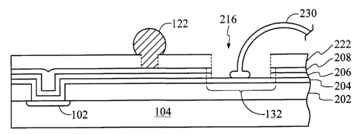
(e. g. wire 230, Fig. 2I) will be bonded in a subsequent
wire bonding operation.
The foregoing preferred embodiment discusses
the use of a copper/nickel/aluminum trimetal layer.
Metals other than aluminum can be used as the bondable
layer, including palladium and platinum. Moreover, it is
possible to attain the solder bump & wire pad arrangement
of the present invention if the uppermost layer of metal
WO 01/35462 CA 02388926 2002-04-04 pCT/USO~/24~g7
is gold. Thus, in an alternative embodiment of the
invention gold is used. With respect to Fig. 2D then, a
bottom-most conductive metal adhesion layer 204 can be
sputtered onto passivation layer 202. Typical adhesion
metals include aluminum and titanium-tungsten (TiW). As
before, the metal layer is etched to form the desired
traces 142 - 148 comprising the redistribution layer and
the added wire bond pads 132 - 138.
Next, a layer of nickel 206 is deposited
followed by a layer of gold 208. As shown in Figs. 2E
and 2F, the second passivation layer 222 is then
deposited and etched to form openings 214 and 216.
Finally, solder bump 122 is formed, Fig. 2G. The
subsequent metal etch step shown in Fig. 2H is not
needed. The reason is that gold exhibits adequate
bonding properties for wire bonding purposes. The upper
layer of gold is therefore retained. However, it is
noted that gold does not solder well, since gold leaches
into the solder during the soldering operation. However,
in this embodiment of the invention where the trimetal
layer is gold/nickel/adhesion (AL or TiW), as the gold
leaches into the solder during the soldering operation,
the solder will encounter the nickel layer. Since nickel
is a solderable metal, the solder bump will be reliably
affixed to its solder bump pad area. Thus, the use of a
gold/nickel layer presents both a bondable and a
solderable layer.
Referring back to Fig. l, various uses of the
added wire bond pads are possible. An added wire bond
pad can simply be placed atop its corresponding
underlying wire bond pad. Thus, bond pad 134 is located
atop bond pad 102A. This configuration is used when the
underlying pad 102A does not need to be relocated.
Another use arises in flip-chip configurations. A
connection from the upper chip can be made to a bond pad
on the lower chip to bring out the signal to an external
WO ~l/35462 cA 02388926 2002-04-04 pCT/[Jg00/24087
_8_
pin. Thus, solder bump 126 would be coupled to a
coincident conductive via on an upper chip providing a
connection to pad 136 on the bottom chip by way of trace
146. Yet another use might arise in highly complex
applications where the circuit density is high. One can
imagine a situation where it is desirous to route
underlying bond pad 102B to a new location such as pad
136. However, such a direct routing may not exist due to
the density of the circuitry. The present invention,
however, provides an arrangement whereby pad 102B is
routed to an upper chip in flip-chip design via trace 144
and solder bump 124. The upper chip carries the signal
to solder bump 126 which then continues on to pad 136 via
trace 146. It can be seen from these examples that
numerous applications of the redistribution layer are
contemplated, limited only by the artisan's imagination.
The invention lies not with the particular patterns
possible in the redistribution metallization, but rather
in the fact that solder bumps and wire bond pads can be
combined to provide additional flexibility in terms of
connectivity within a semiconductor device and between
two flip-chip connected die, and in the way the
redistribution metallization is formed to allow both
solder bumps and wire bond pads in the first place.