Note: Descriptions are shown in the official language in which they were submitted.
CA 02389347 2002-04-25
WO 01/40836 PCT/US00/32625
-1-
PHOTODEFINITION OF OPTICAL DEVICES
This application claims the benefit of U.S. Provisional Application
No. 60/168,572, filed December 2, 1999 and incorporated herein by reference.
This invention was made with Government support under Contract No.
N61331-96-C-0036 awarded by the U.S. Navy, Naval Surface Warfare Center. The
Government has certain rights in the invention.
BACKGROUND OF THE INVENTION
Field of the Invention
This invention relates to methods for producing optical waveguides, and
other such components or devices which require patterns of altered index of
refraction or thickness in transparent polymer multilayer structures. In
particular
this invention relates to methods for producing such optical waveguides, and
other
such components or devices upon irradiation with actinic radiation and
subsequent
treatment. These optical waveguides, and other such components or devices may
be used in fields ranging, for example, from telecommunications, to optical
computing, data storage, displays, and sensors.
Description of Related Art
Cun ent technology for manufacturing polymer optical waveguides includes
techniques well known in the art, such as, for example, reactive ion etching
(RIE)
or laser ablation of the core or cladding layers to provide rib waveguides,
ion
implantation, or photobleaching of the core or cladding layers. In addition,
optical
waveguides can be formed by photodefmition, a process in which a layer of
organic
material, for example a polymer, is deposited on another layer of material,
and
predetermined regions of the polymer layer are subjected to actinic radiation
in
order to alter the refractive index of these regions.
CA 02389347 2002-04-25
WO 01/40836 PCT/US00/32625
-2-
The first step in the photodefinition process is the deposition of one or more
transparent photosensitive monomers onto a substrate. The chosen monomers are
selected on the basis of their ability to dimerize or polymerize upon exposure
to
light and their relative indices of refraction. When such monomers are
subsequently irradiated with a pattern of light, for example ultraviolet (UV)
light,
polymerization is initiated in the exposed material. Since the polymer is
formed
from reacted monomers, monomer concentration is depleted in the irradiation
region, creating a gradient in chemical potential between the exposed and the
unexposed areas. The resulting gradients are unstable, and the smaller-
molecular-
weight monomers surrounding the photochemically reacted material will diffuse
as much as possible into the polymerized regions, increasing the index and
creating
a feature in the planar layer. At least a single, subsequent exposure of the
entire
material system to high-intensity UV or thermal radiation, for example, may be
used to complete the process. This fixing step polymerizes all remaining
reactants,
creating a system that is effectively fully cured and inert. An important
aspect of
this procedure is that the resulting physical density in the patterned
(exposed)
regions is either higher or lower than in the unpatterned material. This
density
difference causes an associated difference in index of refraction. Importantly
for
photonic devices, this index change is stable against further processing and
pronounced enough to enable efficient waveguiding. A process of creating
optical
waveguides by photoinduced diffusion is described by Chandross et al. (U.S.
Pat.
Nos. 3,809,732; 3,809,696; 3,993,485, and; 3,953,620, all of which are
incorporated herein by reference) and has been used extensively to create
photonic
devices.
It should be noted that photo-imaging might also be considered to be a form
of photodefinition. In this process, an imaging layer is deposited on a
substrate,
and an image transferred into the surface of or throughout the entire imaging
layer.
The imaging layer in this instance would contain the photosensitive molecules.
This technique would enable, for example, a waveguide to be fabricated by
coating
CA 02389347 2002-04-25
WO 01/40836 PCT/US00/32625
-3-
a substrate/lower cladding layer with photoresist or electron beam sensitive
material such as PMMA, impinging light from a suitable light source (e.g.,
light
in an ultraviolet region) upon a photomask having a predetermined pattern to
transfer the pattern to the photoresist, and developing the photoresist to
provide
photoresist having the predetermined pattern. In this case, the predetermined
pattern is the pattern for the rib/core of the waveguide, and material from
the
imaging layer has been removed to leave the free-standing feature. The
waveguide
fabrication is completed by depositing additional layers) over the patterned
rib/core layer, these layers being additional core or cladding layers. It will
be
appreciated, that the optical feature, or rib, described here, is not
dependent upon
diffusion for its definition.
To applicants' knowledge, the prior art of photodefinition of polymer
optical waveguides requires that the photodefinition process occur effectively
immediately following the deposition of the photodefinable layer, and before
deposition of the upper cladding layer, unless this is to be the photodefined
layer.
Consequently the photodefinition process necessitates that the layer
coating/deposition process be interrupted and intermediate photodefinition
processes or other processing and treatment effected before coating is finally
resumed to complete manufacture of the device. Interruption of the coating
process
to perform photodefinition may ultimately lead to higher loss waveguides due
to
dust or dirt being deposited either at, or in close proximity to, the optical
layer
during processing, and a greater chance of the generation of defects in or
near the
optical layer due to the number of photodefinition processing steps that must
be
performed directly thereon.
Figs. 1 a to 1 d illustrates schematically the technique by which
photodefinition is conventionally practiced in the prior art. As shown in Fig
1 a, the
lower cladding 102 is deposited on the substrate 103 and cured, and a core
layer
104 is then deposited over the lower cladding 102. The core layer 104 is then
optically patterned, for example byphotodefinition, as illustrated in Fig. 1
c. In this
CA 02389347 2002-04-25
WO 01/40836 PCT/US00/32625
-4-
example the optical patterning is lithographic, in which radiation 105
projected
through a mask 106 is used to pattern the optical elements. Alternatively the
exposure can result in a chemical change followed by removal of residual
polymer/monomer using a wet etch, laser ablation, or further processing, to
leave
a rib waveguide (not shown). This step produces an area of elevated or reduced
refractive index, 108, Fig. 1 c. If necessary, the core layer is then locked
or
stabilized using suitable thermal or radiation exposure processing such that
further
refractive index change is unattainable. An upper cladding layer 110 is then
deposited and cured, as indicted by Fig. 1 d. It will be apparent that in this
process,
the layer 104 to be patterned, is processed to achieve photodefinition before
subsequent layers) 110 are applied. This interruption in the layer coating
process
may ultimately lead to higher loss waveguides due to dust or dirt being
deposited
either at, or in close proximity to, the core/upper cladding interface during
the
photodefinition processing steps, or in processing, planarization or
uniformity
problems. It should be noted that the terms upper and lower are used herein
solely
for convenience in refernng to specific layers. The layers they refer to are
not
intended to change if the structure is turned upside down or tilted.
The present invention provides optical waveguides, components or devices
that may be defined after a complete optical multilayer structure/stack has
been
deposited. In addition, the utilization of multiple photosensitive molecules
enables
the required change in index for waveguide fabrication and increased ease of
processing (e.g., fewer processing steps, better adhesion). Furthermore, the
invention allows for a continuous or progressive fabrication process to be
considered, enabling the reduction, if not the elimination, of the need to
interrupt
the coating process to perform waveguide photodefinition and/or not requiring
the
interruption of a continuous (roll) manufacturing multilayer structure/stack
deposition process. Utilization of the current invention enables several
advantages
to be realized. These advantages include, for example, the following: lower
loss
waveguides due to less dust/dirt being deposited in, or in close proximity to,
the
CA 02389347 2002-04-25
WO 01/40836 PCT/US00/32625
-5-
optical layer during processing; the option for the deposition/coating
processing to
be performed independently from waveguide photo-patterning and the potential
for
increased ease of overall processing including a decreased number of
fabrication
steps and improved interlayer adhesion as a result of the uninterrupted layer
coating
process. This invention also has the flexibility to be used to position and
create
channel waveguides exactly where required within a multilayer structure to
interconnect components.
SUMMARY OF THE INVENTION
According to the invention, roughly described, an optical structure is
fabricated by forming an active layer including a photodefinable material on a
substrate or on another underlying layer, forming an upper layer above the
active
layer, and then patterning the active layer by selective application of
radiation
through the upper layer. The upper layer is substantially transparent to
radiation
of the type required to activate the photodefinable material in the active
layer.
BRIEF DESCRIPTION OF THE DRAWINGS
The invention may be more fully understood from the following detailed
description thereof taken in connection with the accompanying drawings which
form a part of this application and in which:
Figs. 1 a -1 d (collectively Fig. 1 ) is a schematic outline of the methods
steps
of a conventional photodefinition process.
Figs. 2a - 2e (collectively Fig. 2) is a schematic outline of methods steps
that may be used to implement the current invention.
Fig. 3 illustrates the optical response characteristics of two
photoinitiators.
Figs. 4 (a) and 4(b) (collectively Fig. 4) experimentally show the observed
mode profile for waveguides created via reactive ion etching and via the UV
photodefinition process of the current invention, respectively.
Fig. 5 illustrates a multilayer optical stack incorporating two core layers.
CA 02389347 2002-04-25
WO 01/40836 PCT/US00/32625
-6-
Fig. 6 is a magnification of a selected region of Fig. 5 illustrating coupling
between the two core layers.
Fig. 7 is a perspective view of a thermo-optic grating device fabricated
according to the invention.
Fig. 8 is a flow diagram illustrating how a multilayer structure can be
fabricated on a web.
Fig. 9 illustrates schematically a "conveyor belt" type fabrication process
for further processing a multilayer structure fabricated on a web.
Fig. 10 illustrates schematically an optical waveguide display system
incorporating applicators and electrical interconnect vias.
Fig. 11 illustrates schematically an add-drop mux-demux for WDM
communication systems.
Fig. 12 illustrates another embodiment of a multilayer optical. stack
incorporating two core layers.
DETAILED DESCRIPTION
A schematic representation of an embodiment of the current invention is
illustrated in Figs. 2a to 2e. In essence, the figures show a process in which
an
interior layer of an optical multiple layer stack is photodefined in the
presence of
at least one over-layer and an optional under-layer. The layer that is
ultimately to
be photodefmed is therefore "protected" during the photodefinition process
from
the incorporation of dust or other foreign bodies, the creation of extrinsic
surface
flaws and consequently has the potential to support lower loss optical
waveguides.
In addition, an uninterrupted layer coating process offers the prospect of
improved
interlayer adhesion properties. The lower number of defects attainable by such
processing ultimately leads to fewer failure modes, higher yield of fabricated
optical waveguides and an improved product quality.
Implementation ofthe process illustrated in Fig. 2 involves an interior layer
polymer chemistry system that satisfies two general requirements: firstly the
CA 02389347 2002-04-25
WO 01/40836 PCT/US00/32625
_ 'j _
interior layer should be stable enough to have an upper layer placed over it,
and be
coated on a lower layer if desired; secondly, that it remain active enough to
be
controllably patterned, even after the upper layer has been placed over it.
In accordance with an embodiment of this invention, the process for
creating an optical polymeric waveguide may comprise the steps of: (a)
creating an
optical multiple layer stack, mechanically and chemically stabilized; (b)
patterning
with radiation, for example UV light, to activate a plurality of
photosensitive
molecules such that they enable an optical device to be defined; and (c)
locking the
final structure permanently with radiation to substantially prevent future
unwanted
refractive index changes.
In accordance with the preferred embodiment of this invention, the process
for creating an optical polymeric waveguide may comprise the steps o~ (a)
creating
an optical multiple layer stack, mechanically and chemically stabilized e.g.
by
activating a first type ofphotosensitive molecule by exposure to a first
wavelength,
which may be, for example, visible light, causing sufficient linking of the
polymer
molecules to at least prevent the layers of the stack from flowing; (b)
patterning
with a second wavelength of light, for example with ultraviolet (UV) light,
the
second wavelength activating a second type of photosensitive molecule which
enable an optical waveguide to be defined; ( c) optionally enhancing the
diffusion
or crosslinking process by, for example, baking the optical stack; and (d)
locking
the final structure permanently, with a third wavelength of light, a
wavelength
which may be different from the second wavelength used, for example with
ultraviolet light. The aim of this step is to activate at least any of the
first type of
photosensitive molecule, and preferably any of the second type of
photosensitive
molecule that have not previously been activated, effectively locking the
final
structure and substantially preventing future unwanted refractive index
changes.
These steps are illustrated schematically in Fig. 2.
CA 02389347 2002-04-25
WO 01/40836 PCT/US00/32625
_g_
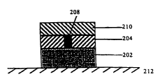
Creating an optical multiple layer stack
In this embodiment of the invention, the optical multilayer stack is
constructed by forming one layer on top of the next. The optically transparent
polymer lower cladding layer 202 lies on an optional substrate 212. This
support
S prevents mechanical failure of the film, such as breakage or wrinkling that
would
affect the surface quality and uniformity during and following processing. The
optional substrate 212, the support layer, may be either some form of
inflexible
material such as glass, sapphire or silicon, or a flexible web-like material
such as
Mylar~ or Kapton~. It will be apparent that if no substrate is provided, a
portion
of the lower cladding 202 itself may act as the support material.
The lower cladding 202 is preferably a crosslinked polymer, for example,
an (acryloxypropyl)methylsiloxane-dimethylsiloxane copolymer (available from
Gelest, Inc. of Tullytown, PA as product code UMS-992), or may alternatively
comprise an inorganic or non-crosslinked organic material, for example silica
glass, polymer, semiconductor, sol-gel, aero-gel, liquid crystal, self
assembled
monolayer or ceramic. A crosslinked polymer is defined as a network formed by
a multifunctional monomer/polymer. In a loosely-crosslinked material, local
freedom of motion associated with the small-scale motion of chain segments is
retained, but large-scale movement (flow) is prevented by the restraint of a
diffuse
network structure. The crosslinked network extending throughout the final
article
is stable to heat and cannot be made to flow or melt under conditions that
would
cause linear (not crosslinked) polymers to flow or melt.
The lower cladding 202 may be deposited on the substrate by one of the
many available methods known in the art (dependent on the material used), such
as for example spin, meniscus, extrusion, spray, dip, slot-die, or flash
evaporation
coating for polymer materials, vacuum deposition (e.g. evaporation,
sputtering,
chemical vapor deposition, CVD, or plasma enhanced CVD) for hard oxide or
nitride materials such as SiOz or SiNX. The top surface of the resulting lower
cladding layer (the surface furthest from the substrate) should be optically
smooth
CA 02389347 2002-04-25
WO 01/40836 PCT/US00/32625
-9-
and defect free so as to result in low scattering of the optical mode at the
core
cladding interface and subsequently lead to a low optical waveguide
propagation
loss in the integrated optical circuit. In addition, the cladding layer
material itself
should inherently exhibit low absorption and scattering at the wavelengths) to
be
guided in the optical structure.
It is preferable that, once deposited, this lower cladding layer be stable,
that
is of a consistency such that it does not flow over or into the substrate, and
that it
is both structurally and chemically able to receive the core layer above it
without
being adversely structurally or chemically affected, i.e., rendered incapable
of
acting as a waveguide cladding layer, or preventing an overlying layer from
operating in its desired photodefinable manner. For lower cladding materials
that
do not inherently exhibit these properties in the as-deposited state, it is
preferable
that they be at least partially cured to achieve these properties. Partial
curing
means treating or processing such that further reaction during or following
processing may be allowed if appropriately activated and desired. The at least
partial curing may be accomplished by incorporating a plurality of
photosensitive
molecules of a first type, the photosensitive molecules comprising
photosensitive
monomers, charge transfer agents, photoinitiators or other such molecules that
can
be activated at a selected wavelength, 7~L~, or range of wavelengths, in the
lower
cladding material. For example, this first type of photosensitive molecule may
be
activated at a long wavelength such as that of visible light with a wavelength
greater than 430nm. Once deposited, e.g., by sputtering, the lower cladding
polymer layer may then be exposed to this visible light, by for example a
conventional lamp/filter combination, causing sufficient linking of the
molecules
such that the material is prevented from flowing or swelling. The inclusion of
such
a first type of photosensitive molecule enables the lower cladding layer, once
deposited, to be at least partially cured, that is to substantially retain its
thickness
and uniformity despite subsequent processing.
CA 02389347 2002-04-25
WO 01/40836 PCT/US00/32625
- 10-
An optical core layer 204, preferably a polymer layer as described below,
is next applied over the lower cladding layer 202 to ultimately provide an
optical
waveguiding structure. At this stage, the refractive index difference between
the
as-deposited core and the upper and lower cladding layers, combined with the
thickness of the core layer, does not have to be sufficient to provide
confinement
for at least one propagating mode of the structure, but the material selection
does
enable such confinement once the subsequent photodefinition process has been
completed. Hence, the portion of the core layer that has been subsequently
photodefined has a refractive index that is different, that is either greater
or less,
than either of the cladding layers. However, the present embodiment uses
different
starting (as-deposited) indices in the vertical direction for the di fferent
layers of the
optical structure, and employs the photodefinition diffusion process to create
lateral
waveguide mode confinement: In addition, the thickness and the refractive
index
difference between the core and cladding layers should preferably be
sufficient to
ensure that the evanescent field of the optical mode in the cladding layer has
decayed away to substantially zero before it reaches the outermost boundary of
the
cladding, in order to minimize propagation or absorption losses and the effect
of
the environment. However, for situations in which it is desirable that the
waveguide mode interact with the cladding surface or features adjacent
thereto, for
example electrodes, it may not be necessary for the evanescent mode to decay
to
such a value. Equations for determining appropriate optical thickness are well
known in the art, and can be found, for example, in Nishihara et al., "Optical
Integrated Circuits", McGraw Hill, 1989, incorporated herein by reference in
its
entirety.
The deposition process for the core layer is again dependent on the material
choice, as for the lower cladding layer. Suitable choices for the core layer
are
polymer materials such as Norland Optical Adhesive 68, PMMA, or a suitably
selected crosslinkable polymer. The selected material should be able to
provide a
different refractive index (i.e. higher or lower) than both the cladding
layers (at
CA 02389347 2002-04-25
WO 01/40836 PCT/US00/32625
-11-
least once photodefinition has been completed) and possess sufficient optical
transparency (low absorption and scattering losses) for the desired
wavelengths)
to be propagated through the optical structure, with acceptably low losses
(acceptable loss is determined by the exact device design and function). In
addition, this core layer should have a low surface roughness to prevent
excess
propagation loss due to scattering at the interlayer interfaces.
As for the lower cladding 202, a limited or partial cure of the core layer 204
may be advantageous depending upon the material utilized. Such limited or
partial
curing may be preferred in the case where the core layer is to be
photodefined. In
this instance, the partial curing of the polymer prior to the photodefinition
step
enables sufficient crosslinking to prevent the material from flowing,
swelling, or
chemically interacting with the other layers, hence providing for a robust
structure
capable of being rolled up (provided that the substrate is not rigid) and
stored in a
pre-patterned state. However, the crosslinking is not sufficient to entirely
prevent
1 S subsequent diffusion or further crosslinking from occurnng after
appropriate
processing. The partial cure may be performed at either the same wavelength
7~Lc
as the lower cladding 202, or a different wavelength ~,c, It will be apparent
that if
partial curing of the core layer 204 is to occur at the same wavelength as the
lower
cladding 202, the same first type of photosensitive molecules may be
incorporated
into the core layer 204 on deposition.
In addition to this first type of photosensitive molecule, the core layer 204
in this embodiment is preferred to comprise a second type of photosensitive
molecule. This second type of photosensitive molecule may comprise a
photosensitive monomer, charge transfer agent, photoinitiator or other such
molecules, that is activated at a second wavelength distinct from the first
wavelength, for example a UV wavelength. It is this second type of
photosensitive
molecule that will later be utilized for creation of the optical waveguide. In
general, the greater the concentration ofthe second type ofphotosensitive
molecule
in the core layer material, the greater the refractive index change achievable
upon
CA 02389347 2002-04-25
WO 01/40836 PCT/US00/32625
-12-
later photodefinition up to the limit imposed by the number of total bonds
which
can form in the polymer. Preferably the second type of photosensitive molecule
concentration should be in the range of 0.1 % to 20 % by volume of the core
layer
material, but it may be as high as 80%. It is important that a response, e.g.,
the
absorption wavelength, of the second type of photosensitive molecule be either
above or below some threshold set by the properties of the first type of
photosensitive molecule. In this manner, it can be arranged such that
substantially
only one of the first or second types of photosensitive molecules will respond
at a
given wavelength.
Fig 3 shows the spectral responses of two hypothetical types of
photosensitive molecules, specifically for incorporation in the embodiment of
Figs.
2a-2e, a first type of photosensitive molecule 302 and a second type of
photosensitive molecule 304. Their different response characteristics can be
exploited to effect separate activation by exposing them to different
wavelengths
of light. The first type of photosensitive molecule 302, with its strong
response at
a longer wavelength 306, is activated first using a lamp/filter combination
with a
sharp wavelength cutoff below some lower threshold set by the properties of
second type of photosensitive molecule 304. This first wavelength exposure
does
not substantially affect or activate this second type ofphotosensitive
molecule 304,
although there may be a weak absorption by the second type of photosensitive
molecule, possibly inducing a small activation of that species. After the
first
activation reaction due to the first type of photosensitive molecules has
proceeded,
either partially or to completion, the second type of photosensitive molecule
304
can be activated to induce curing at some later time using a second exposure
at a
shorter wavelength 308. Note that because of the short wavelength absorption
tail
associated with the first type of photosensitive molecule 302 (a general
characteristic of a broad variety of polymers), it is preferable that the
sequence of
exposures is not reversed.
CA 02389347 2002-04-25
WO 01/40836 PCT/US00/32625
-13-
It should be noted at this stage that the amount of the second type of
photosensitive molecule present in the photodefinable layer influences the
refractive index change and thus optical mode width achievable within the
photodefined waveguide. The greater the amount of the second type of
photosensitive molecule used in the core layer, in general, the higher the
refractive
index change caused by photodefinition and the narrower a mode shape that may
be achieved, up to some limit set by the maximum differential refractive index
that
can be created in the material using the preferential curing invoked by the
patterned
exposure. The degree of cure (that is the extent of reaction, defined by the
number
of bonds formed as a fraction of the total number of bonds capable of forming)
of
the core layer 204 polymer is positively proportional to the curing energy
applied,
or alternatively to the amount of the photosensitive molecule species that is
activated by exposure to radiation. The partial degree of cure which is
applied to
the core layer after deposition to make it chemically and mechanically stable
and
robust, is an important factor in achieving a narrow waveguide mode width and
high quality channel waveguides by the photodefinition process described
herein.
The narrowest most highly confining waveguide is generally achieved by
applying
the lowest degree of partial cure which is still compatible with the chemical
and
mechanical stability required by the core layer film. A final locking step
(discussed
below) is then preferably administered to ensure chemical, thermal and
physical
stable devices result.
Following the core layer deposition and pre-cure, an upper cladding 210,
which maybe comprised, for example, of another (acryloxypropyl)methylsiloxane-
dimethylsiloxane copolymer (available from Gelest, Inc. as product code UMS-
182), is provided to isolate the optical mode from actuators or the effects of
the
environment. The combination of the refractive index difference between the
core
and the upper cladding (at least after photodefmition has been completed) and
the
upper cladding thickness should be sufficient to cause the evanescent field of
the
optical mode to have decayed to substantially zero before it reaches the outer
CA 02389347 2002-04-25
WO 01/40836 PCT/US00/32625
-14-
surface of the cladding to prevent absorption losses from occurnng in
overlying
areas. Alternatively, if it is desired that the mode interact with features or
materials
(e.g. a chemical species in a sensor) outside the optical multilayer stack,
the top
cladding thickness and refractive index may be chosen such that the evanescent
field of the mode has a predetermined strength at the upper cladding top
surface to
provide a desired mode interaction. Other suitable choices for the upper
cladding
layer 210 material include crosslinkable polymers, inorganic or non-
crosslinked
organic material, for example silica glass, polymer, sol-gel, aero-gel, liquid
crystal
or self assembled monolayer. The chemistry and the method of deposition
utilized
for this upper cladding layer should be such that its deposition does not
deform or
otherwise damage the core layer on which it lies, or render it incapable of
further
photodefinition if desired.
Once again, partial curing of this layer may be desirable, either at the same
wavelength ~,L~ as the lower cladding, the core layer ~,c , or a different
wavelength
~,U~. It will be apparent that if partial curing of the upper cladding layer
is to occur
at the same wavelength as the lower cladding, the same first type
ofphotosensitive
molecule may be incorporated into the upper cladding layer on deposition. In
addition, it is important that the partial cure of the upper cladding layer
should not
significantly increase the level of cure of the core layer, at least not to
such an
extent as to interfere with the later photodefinition process.
In this manner, all three materials of the lower cladding layer, core layer
and upper cladding layer may be at least partially cured, creating a temporary
controllable chemistry in a predetermined manner. The temporary controllable
chemistry means that the chemical and physical nature of the three materials
is
sufficiently stable that they can form the multilayer structure described, but
that
they can be further processed if so desired. The materials are thus initially
selected
such that when at least partially cured, they are able to be substantially
stable both
structurally and chemically. It should be noted that fabrication of the
multilayer
stack has been discussed as possibly requiring at least partial curing of the
three
CA 02389347 2002-04-25
WO 01/40836 PCT/US00/32625
-15-
layers. Hence it will be apparent that fabrication of the stack may allow for
the
upper and lower cladding layers to be fully cured, but the core layer, and any
other
layer that is desired or designed to be photodefined, is not fully cured prior
to
waveguide photodefinition.
We believe that the resulting mode profile diameter of an optical waveguide
formed utilizing a photodefinition process according to the embodiment
described
herein decreases as the energy that is applied to the partial cure decreases.
Note,
however, that the mode profile diameter is also dependent upon other
parameters,
for example the core layer thickness, the cladding refractive index etc.
It should be noted that although the description above discusses a three
layer optical stack, the substrate/lower cladding, core and upper cladding
layers,
many more layers may be added to the structure. In particular, many more
layers
may be placed either above or below the core layer, and patterned with UV
light
as described herein. Except where the context requires otherwise, the terms
"above" and "below" are intended to be interpreted transitively. That is, one
layer
is considered to be "above" or "below" a second layer, even if there is an
intervening layer between the first and second layers. In addition, in the
embodiment described, the refractive indices of the upper cladding, core and
lower
cladding layers are portrayed as having their own individual refractive
indices,
however it is quite possible that the upper and lower cladding layers have the
same
refractive index, and it is possible that the core layer, prior to the
patterning step,
have the same refractive index as either or both of the cladding layers. In
this case
the core layer would have a photosensitive molecule that will enable the
photodefinition process to occur. It is therefore possible that all three
layers, the
lower cladding, upper cladding and core comprise the same material, and have
substantially the same refractive index prior to photodefinition, the core
layerbeing
distinct in that it also comprises at least first photosensitive molecules.
The method set forth above is presented as a non-limiting example of a
technique for fabricating an optical multilayer stack. Other fabrication
methods will
CA 02389347 2002-04-25
WO 01/40836 PCT/US00/32625
-16-
be apparent to those skilled in the art. For example, an optical multilayer
stack may
be created by the process of lamination. In this process, the at least
partially cured
lower cladding, core and upper cladding layers are laminated by placing them
in
contact with one another and controllably applying pressure uniformly such
that the
air between the layers is substantially removed. At this stage, after
lamination, no
photodefinition to create the waveguide has yet occurred, and the lamination
process has played no part in the diffusion process.
Patterning with ultraviolet light, photodefining
Once the optical multilayer structure has been constructed, the optical
waveguide, which may take any desired dimensional shape in the plane of the
photodefined layer, for example a planar or channel waveguide, is created by
the
process of photodefinition. The waveguide pattern desired may be defined by a
mask 206, which has at least a patterned area through which actinic or other
radiation 205 can pass. The mask 206 can be, for example, a conventional layer
of photoresist, opaque at the wavelength of the second cure, which has been
exposed and etched to the desired pattern. Once the mask has been placed or
fabricated (e.g., in a lithographically patterned metal or resist layer) on
the
uppermost surface of the upper cladding layer 210, a UV light source or other
suitable source is aimed to direct radiation towards the masked surface. In
embodiments where exposure to radiation (preferential cure) leads to an
increased
refractive index region, optical waveguides are created in the areas through
which
actinic radiation can pass, and not in areas void of illumination (i.e., those
regions
covered by the opaque portions of the mask 206).
Alternatively, a projection or proximity exposure system can be utilized
whereby the mask never contacts the surface of the polymer, but the pattern is
imaged either using lenses or collimated light into the polymer to have
substantially the same effect as the contact process. Equally, a direct write
process
could be used where a focused beam ofradiation, for instance a UV laser
(excimer)
CA 02389347 2002-04-25
WO 01/40836 PCT/US00/32625
-17-
or electron beam, is scanned across the surface of the polymer layers to
define the
irradiated pattern, possibly also utilizing intensity modulation to control
the exact
position of the features in the waveguide network.
In this photodefinition step, uniformity of the radiation beam cross-section
as it descends upon the uppermost surface of the upper cladding, through the
mask,
is desirable. Such uniformity aids in the uniformity of the refractive index
variation achieved throughout the volume, and the uniformity of the optical
waveguide network formed by the photodefinition process.
The radiation 205 passes through the open areas of the waveguide mask
206, through the upper cladding layer 210 and into the core layer (or
photodefinable layer) 204. In this selected volume of the core layer, the
volume
exposed to the radiation 205, the second type of photosensitive molecule is
"activated" by the actinic radiation, and an optical waveguide is formed.
The waveguide network can easily be defined to any desired two
dimensional shape in the plane of the photodefined layer, by appropriately
fabricating the mask 206, waveguide structures including curves, X- and Y-
branches, and parallel couplers can be created. The waveguide created may
support either multiple transverse optical modes or a single transverse mode,
depending on the strength of the optical confinement and the dimension of the
guide. In general, an optical mode is distinguished by its electro-magnetic
field
geometry in two dimensions, by its polarization state, and by its wavelength.
If the
index of refraction change experienced by the optical mode is small enough
(e.g,.
0n = 0.003) and the dimensions of the guide are narrow enough (e.g. 5.0 Vim),
the
waveguide will only contain a single transverse mode (the lowest order mode)
over
a range of wavelengths. For larger refractive index differences andlor larger
waveguide physical dimensions, the number of optical modes increases.
Preferably
the waveguide is designed to support only a single, lowest order, mode,
eliminating
the complexities associated with higher order modes. Higher order modes have
different propagation constants than lower order modes, and higher scattering
loss,
CA 02389347 2002-04-25
WO 01/40836 PCT/US00/32625
-18-
which can be problematic in some applications. In other applications where
higher
power is desired, higher order modes might be more beneficial.
It will be apparent that although the description above discusses an
embodiment in which the core layer includes the second type of photosensitive
S molecules and thus provides the refractive index change to create the
waveguide,
embodiments in which the cladding layer includes the second type of
photosensitive molecules are also possible. In these embodiments a structure
known in the art as a "strip-loaded" waveguide may be created. On exposure of
the
selected volume of the chosen cladding layer, (for example the upper or lower
cladding layer) activation ofthe second type ofphotosensitive molecule and
further
polymerization occurs, increasing its refractive index, which may also be
accompanied by diffusion of second type ofphotosensitive molecule and monomer
into the selected volume of the cladding layer. The rib of increased index
located
adjacent to the planar core layer induces a channel (or a three dimensional)
optical
waveguide, (see, for example, the aforementioned Nishihara et al. reference).
The
refractive index change in the selected volume of the cladding (together with
any
associated refractive index decrease in the adjacent cladding areas) must be
taken
into account in the design of the waveguide to ensure single mode (or multiple
if
desirable) propagation. Note that the rib of increased index does not have to
be
localized adjacent the core, but may extend through the entire thickness of
the
cladding layer.
Alternatively, the photodefinable layer does not have to fulfill the function
of either the core or upper cladding layers. By placing a thin photodefinable
layer
adjacent the core layer (above or below), the rib of increased refractive
index
described above may be created by photodefinition. However, the optical mode
is
not confined within the photodefined layer itself, but rather within the adj
acent core
layer, the rib providing lateral confinement and guiding. Note also that the
rib does
not provide the cladding layer functionality as it is not sufficiently thick
to isolate
the optical mode and is therefore itself placed adjacent the cladding layer.
CA 02389347 2002-04-25
WO 01/40836 PCT/US00/32625
-19-
In order to photodefine waveguides in a multilayer polymer structure, it is
preferable to photoinduce index changes in one layer to the relative exclusion
of
changes in the other layers which, in general, lie above and below the one of
interest. However, as long as the refractive index changes in the various
layers are
controllable and predictable it is possible to create waveguide structures
while
allowing refractive index changes to occur in more than one layer as a result
of the
same exposure.
The process described above, preferably utilizing a polymer comprising at
least two types of photosensitive molecules can be utilized to create a high
quality
optical waveguide by creating the channel waveguide directly in the core
layer,
through the upper cladding layer. In particular, it utilizes two types of
photosensitive molecules with different spectral responses. The first type of
photosensitive molecule is selectively activated to at least provide a partial
cure
level to structurally fix the multilayer stack so it can be safely handled,
stored and
distributed. The second type ofphotosensitive molecule is later used to
photodefine
the layer of interest.
It will be apparent that this invention is not limited to the utilization of
only
two types of photosensitive molecules. A third type of photosensitive
molecule,
for example, may be included, enabling even further photodefinition to be
possible
in a subsequent step. The third type of photosensitive molecule would react to
a
third wavelength of light different from that of the first and/or second types
of
photosensitive molecules. Similarly, fourth, fifth, etc. types of
photosensitive
molecules may be incorporated into the design and fabrication process.
In an alternative embodiment, there is no requirement for the core (or
photodefinable) layer to comprise two different types of photosensitive
molecule.
In such an embodiment partial cure of the lower cladding layer may be induced
thermally, or by activation of a first type of photosensitive molecules. The
core
layer is then deposited, the core layer comprising a second type of
photosensitive
molecules. In some embodiments the first and second photosensitive molecules
CA 02389347 2002-04-25
WO 01/40836 PCT/US00/32625
-20-
may be of the same type. Partial cure of the core layer may be achieved by
activating some of the second type of photosensitive molecules, or by thermal
or
electron beam curing methods. The deposition process and partial curing
process
of the upper cladding layer must be chosen such that they do not substantially
or
adversely affect the level of cure in the core (photodefinable) layer. That
is, if a
photoexposure is used to activate a type of photosensitive molecule in the
upper
cladding layer, that exposure should not affect the level of cure in the core
layer
such that photodefinition cannot be achieved with a subsequent patterned
exposure
of appropriate wavelength to activate the type of photosensitive molecules in
the
core layer. Subsequent photodefinition of the core layer is achieved by
activating
the remaining second type ofphotosensitive molecules, which may be achieved by
exposure to the same wavelength that may have been used in the partial cure
process.
It will also be apparent that this invention is not limited to a process that
requires photodefinition through only the upper cladding layer as described
above.
It is possible to utilize this process by photodefining through any layer, or
some
number of layers, for example the lower cladding layer or the substrate
itself.
It should be noted that wherever the methods described herein call for
photosensitive molecules of a particular type, it will be appreciated that the
molecules of that type can be accompanied by additional molecules of a
different
type, which are activated in the same step as the molecules of the particular
type.
The additional type can be chosen to be activated by exposure to the same
radiation
as the particular type, or alternatively, can be chosen to be activated by
exposure
to a form or wavelength of radiation that is different from that which
activates the
molecules of the particular type. If the additional type is activated by
exposure to
a form or wavelength of radiation that is different from that which activates
the
molecules of the particular type, then different embodiments can provide the
two
types of radiation either simultaneously or sequentially.
CA 02389347 2002-04-25
WO 01/40836 PCT/US00/32625
-21 -
Enhancing the diffusion/crosslinking process
If considered necessary, an optional bake process may be applied to the
multilayer stack to enhance the diffusion or the crosslinking process. This
step is
performed between the patterned photodefinition exposure and the final "lock
up"
exposure provided to secure the waveguide pattern in the polymer structure.
The
range of temperatures and the time for which the heat should be applied will
vary
depending upon the chemical nature of the multilayer stack. It is desirable
that the
heat applied is above room temperature such that molecules are able to move,
yet
not so high that these same molecules evaporate, sublime or otherwise
disassociate
from the multilayer stack, for example, in the range of 25 to 100°C .
The time for
which the heat is applied preferably is long enough to attain equilibrium of
diffusion or crosslinking in the desired region. For the multilayer stack
described
hereinbefore, a bake process carried out at a temperature in the range of 60
to
85 °C, preferably 75 °C, for a time period in the range of 15
minutes to 1 hour,
preferably 30 minutes, is effective in achieving photodefined waveguide
fabrication.
Locking the final structure permanently
It should be noted that prior methodology leaves open the possibility that
unreacted material may remain following processing, which may then further
react
or degrade during use or storage in a manner (i.e., a slow change in
refractive
index) that decreases the device performance. For example, U.S. Pat. No.
4,712,854 (Mikami et al.), incorporated by reference herein, describes a
process in
which the refractive index variation of a photodefined material is controlled
by the
progress of the photopolymerization of the material. Prior art technology
requires
or recommends that the wavelength of the light to be guided be preferentially
outside the wavelength range of photosensitivity, which encompasses the
wavelength of the light to which the sample was exposed (for example) in order
to
CA 02389347 2002-04-25
WO 01/40836 PCT/US00/32625
-22-
avoid further reaction or change in the cross-sectional variation of the index
of
refraction within the guide.
The embodiment of Figs. 2a-2e, provides a final locking step to be
administered to ensure a chemically, thermally and physically stable
waveguide,
both at this stage and following any subsequent processing that might be
performed. The entire structure is exposed to radiation wavelengths) 214, such
that any of the types of photosensitive molecules that have not been activated
are
now utilized, thus completing the curing of any layers which were previously
only
provided with a partial level of cure as described above. Hence, in the
example
given, if all the three layers (the lower and upper claddings, and the core
layer)
included a first type ofphotosensitive molecule which responded to wavelength
~.Lc
exposure to at least this wavelength would be required so that the structure
would
be stabilized. In addition, exposure to ~,c and ~.cc to activate any or all of
the second
type of photosensitive molecules is desirable to prevent further refractive
index
changes. In the above-described embodiment, it is preferable that the
structure is
uniformly exposed at the activation wavelengths of all the types of
photosensitive
molecules incorporated into the three layer structure such that substantially
all the
types of photosensitive molecules in the polymer multilayer structure are
activated.
In this manner, further exposure to actinic radiation in the course of
processing will
not induce any further curing of the polymer layer and will thus not (in
principle)
affect the patterned index structures created by the previous photodefinition
process. Exposure for a time period in the range of 5 to 30 minutes, with the
intensity ranging from 5 to SOmW/cmZ, is considered necessary to lock the
chemical structure without chemically degrading the material. Exposure for 10
minutes at 20mW/cmz is preferable for the materials disclosed above. The range
of intensities and the time for which the radiation should be applied will
vary
depending upon the chemical nature of the multilayer stack. It is desirable
that the
radiation is applied at an intensity to enable activation of the
photosensitive
molecules, but not at an intensity at which destruction of the individual
layers
CA 02389347 2002-04-25
WO 01/40836 PCT/US00/32625
-23-
occurs. The time for which the radiation is applied should preferably be long
enough to achieve full activation of all types of photosensitive molecule and
"complete" cure and may range from approximately a minute to 5 hours.
In terms of the final, lock up exposure, the term "complete" cure represents
the activation of substantially all the photosensitive molecules present in
the
polymer materials, and thus represents a substantially unchanging state of
cure or
bonding, which will not vary significantly over time, as the result of further
processing, or as a result of exposure to guided optical energy of any
wavelength.
It should be noted that it is possible to sensitize the polymer to control the
conditions that influence activation of the photosensitive molecules using
commercial sensitizers such as peroxides like benzoyl peroxide. These
molecules
may be added during processing, or in appropriate cases, following deposition
and
before photodefinition.
Fig. 4 provides a comparative illustration of mode profiles in two different
waveguides, the first waveguide being fabricated using a known reactive ion
etching (RIE) technique, and the second being fabricated by employing the
photodefinition process set forth above. It is found that the mode width for
an
optimized photodefined waveguide profile (Fig. 4(b)) is only about 1 ~m wider
than
for the RIE waveguide profile (Fig. 4(a)). It is believed that the waveguide
created
by the RIE process produces a step-like index profile, and that the waveguide
created by the UV photodefinition process produces a graded (e.g. gaussian)
index
profile.
When light at 980 nm is focused into the guides formed using the process
described above, single transverse mode optical waveguide mode patterns are
observed in the transmitted light. The materials and thicknesses used in one
example are as follows: a Corning 1734 glass substrate; a Gelest UMS-992
polyacrylate lower cladding, layer thickness 5 pm; a Norland Optical Adhesive
68
core, layer thickness 1.2 Vim; and a Gelest UMS-182 polyacrylate upper
cladding,
layer thickness 1.4 pm; with Darocur 1173 (Ciba Giegy) and Irgacure 369 (Ciba
CA 02389347 2002-04-25
WO 01/40836 PCT/US00/32625
-24-
Giegy) as the first and second photosensitive molecules respectively. As fully
processed, the materials used in experimental construction of the three layers
provide indices of refraction of 1.488, 1.522, and 1.422, respectively. The
optical
throughput of a 4cm long waveguide is up to 25% and the mode diameter is 10.5
microns in the plane of the core layer. Thus the present invention is capable
of
providing photodefined optical waveguides suitable for application in novel
integrated optic based flat panel displays, for example, the type of display
described in U.S. Pat. No. 5,544,268 to Bischel et al., incorporated by
reference
herein.
It should be recognized that the foregoing description concerning the
number and ordering ofprocess operations, and series of operations, sets forth
one
exemplary method for constructing one embodiment of the invention. Numerous
alternatives to the aforementioned process sequence, as well as partial
performance
of certain operations or series interlaced with partial performance of other
operations or series, exist and are within the contemplated scope of the
invention.
Discussion of possible mechanisms for change in index
It is well known that photodefined waveguide formation results from an
induced change in refractive index. Prior art for the photodefinition of
waveguides
assumes that small molecule diffusion is required for the definition process
to
occur. Diffusion of some small molecules into the selected volume (the region
undergoing photodefinition) aids in increasing the refractive index, however
it is
believed that there are other mechanisms that may play a part in the
definition
process.
It is known to those skilled in the art that one mechanism for changing the
index of refraction of a monomer/polymer is by reacting it, taking advantage
of the
fact that the polymer has a different index of refraction than the monomer.
The
photodefinition process encourages reactions to occur, including those which
induce polymerization of the monomer within the selected volume. In general, a
CA 02389347 2002-04-25
WO 01/40836 PCT/US00/32625
- 25 -
monomer and a corresponding polymer have different indices of refraction; for
example the indices of methyl methacrylate (npz° - 1.4140) and styrene
(no ° -
1.5470) differ significantly from poly(methyl methacrylate) (npz° =
1.4920) and
polystyrene (nDZO = 1.5916) respectively. In general, forming a network or
crosslinked polymer increases the refractive index even more than forming a
linear
polymer due to the fact that more bonds are formed.
In addition to the monomer polymerization, other photosensitive molecules,
for example photoinitiators, sensitizers, etc., also may be activated and form
crosslinked bonds within the polymer network. The amount of a type of
photosensitive molecule present is partially responsible for controlling the
number
of crosslinked bonds formed, enabling the monomer to crosslink with polymer
(for
example), the number of reactions that occur may therefore be controlled by,
among other variables, changing the photosensitive molecule concentration. The
photosensitive molecule concentration thus affects the final density and index
of
the reacted material, by affecting the number of crosslink bonds formed, up to
the
maximum number that can be supported by the polymer network. A greater
number of crosslink bonds per unit volume tends to pull the polymer chains
more
closely together, compacting the structure and increasing the material density
and
thus increasing the index of refraction. It should be noted that the crosslink
density
may also be changed thermally, radiatively, or by other means, not just via
photodefinition. Incomplete reaction (residual monomer or unactivated
photosensitive molecules) or lowered crosslink density decreases the amount of
index change achievable. However it is also well known that the index change
achieved by this mechanism may be relatively small, and therefore this may not
be
the only mechanism at work in the invention described herein.
A second possible mechanism for changing the refractive index in a
polymer is by increasing the material density of the system in question,
without
necessarily increasing the number of crosslink bonds per unit volume. In the
material system of the multilayered stack described, the polymerization
reactions
CA 02389347 2002-04-25
WO 01/40836 PCT/US00/32625
-26-
described above cause a depletion of both the second type of photosensitive
molecule and/or the unreacted monomer. These depletions produce gradients in
concentration and chemical potential which in turn induce the second type of
photosensitive molecule and/or monomer in the adjacent unaffected (unexposed)
regions) to diffuse into the selected volume. This type of diffusion mechanism
has
been described in the research literature (Colburn et al., Applied Optics, 10,
1636
(1971) and Wopshall et al., JOSA, 61, 649 (1971), both incorporated by
reference
herein). As the monomer diffuses into the selected volume, the density of that
volume increases, increasing the refractive index of the selected volume and
potentially creating an optical waveguide, (provided that for the material of
choice
the refractive index increases with density).
In the embodiment described earlier, in which the core layer of the optical
waveguide included a second type of photosensitive molecules, and the core
layer
had a refractive index that was greater than that of the surrounding cladding
layers,
the following condition should be noted. The diffusion of monomer and the
second type of photosensitive molecules from the adjacent planar core layer to
the
selected volume (to eliminate the concentration gradients and chemical
potential
induced by the activation of the second type of photosensitive molecules and
the
subsequent polymerization of the monomer) may result in a slight decrease in
refractive index of the region directly adjacent the waveguide compared to
that
which would be expected from a uniformly cured planar layer where no volume
was selected for preferential activation of the second type of photosensitive
molecule.
A third possible mechanism for changing the refractive index involves the
diffusion of either a second type of photosensitive molecules, or any reactive
or
unreactive small molecules that differ in refractive index from the final
polymer,
into the selected volume. The unreacted small molecules may be encapsulated,
stable molecules, forming either an interpenetrating network or a semi-
interpenetrating network. In the case of the second type of photosensitive
CA 02389347 2002-04-25
WO 01/40836 PCT/US00/32625
-27-
molecules, this mechanism may increase the refractive index of the selected
volume as the post-activation remnants of the second type of photosensitive
molecules may increase the polarizability of the volume and hence increase the
refractive index.
The effect of photodefinition on Tg
The number of polymer crosslink bonds formed strongly affects the glass
transition temperature, Tg. The glass transition temperature (Tg) is a range
of
temperatures over which significant local motion of the polymer backbone
occurs.
The Tg is usually defined as cooperative motion of about 10 backbone units, or
a
viscosity of 10'4 poise, or a second order phase transition in heat capacity.
The
temperature at which a measured change in slope occurs in the rate-of change-
of
volume with temperature curve, is considered the glass transition temperature
(Tg),
or softening point. For a detailed description see G.B. McKenna, chapter 10,
1 S Comprehensive Polymer Science, Volume 2, Edited by C. Booth and C. Price,
Pergamon Press, Oxford (1989), incorporated by reference herein.
The glass transition temperature (Tg) in any region of a polymer is a
function of the density (p) in that region. In general, as the density
increases, the
index of refraction also increases. Thus the change in density thought to be
associated with the photodefinition process, in addition to causing a
refractive
index change in a photodefined waveguide, should also cause a change in the
glass
transition temperature. The glass transition temperature may therefore be
considered an alternative parameter for qualitatively evaluating the optical
properties of a polymer system.
For example, in an embodiment of the current invention, measurements
taken using the TMA feature of a TA Instruments Atomic Force Microscope-
Thermo-Mechanical Analyzer (AFM-TMA) indicate that the glass transition
temperature of the crosslinked polymer inside the photodefined waveguide
region
is about 20°C higher than that outside the photodefmed waveguide
region. This
CA 02389347 2002-04-25
WO 01/40836 PCT/US00/32625
-28-
change in Tg indicates a significantly higher number of crosslinked bonds in
the
waveguide region.
It may be preferable for the photodefinable layer to comprise a lower Tg,
lightly crosslinked material, where a given absolute change in the amount of
S crosslink bonds may lead to a higher percentage change in material
properties than
in a higher Tg, highly crosslinked material, and thus a more effective
photodefinition process.
It should be noted that the index of refraction of a network polymer may be
a function of processing, i.e. dependent on the method of polymerization. This
is
partly related to the crosslink density achieved (in general the higher the
crosslink
density, the higher the index of refraction) or, in systems where the monomer
or a
type of photosensitive molecule has multiple, similarly reactive sites, the
type of
crosslink bonds formed. Thus, polymer formed using free radical polymerization
as described herein, will potentially have different indices than those formed
using
electronic beam cures, anionic or cationic polymerizations, etc. This is not
important as long as the material indices of the different layers after curing
are
correctly chosen to form the desired waveguide structure after
photodefinition.
Bumps
In the prior art, photodefined waveguides have generally been accompanied
by swelling or bumps on the surface of the photodefined (core) layer. These
are
believed (as discussed in Ashley et al., IEEE Photonics Tech. Lett., 4(9) 1026
(1992), incorporated by reference herein) to result from indiffusion of
monomer
into the selected volume locations where activation of the photosensitive
molecules
causes polymerization to occur. The indiffusion of the monomer during the
curing
or crosslinking process causes the selected volume to swell under certain but
not
all conditions. The presence of the bump may result in enhanced waveguiding by
confining the beam more tightly to the waveguide channel. However,
difficulties
associated with the planarization of overlying layers may more than offset
this
CA 02389347 2002-04-25
WO 01/40836 PCT/US00/32625
-29-
advantage, and consequentlyphotodefinition has not been as widely utilized to
date
as one might otherwise imagine. One of the major attributes of the approach
described herein (utilizing two types of photosensitive molecules) is that it
can
effectively minimize or substantially eliminate the diffusion-induced bump. By
partially curing the polymer layer to be photodefined prior to the patterning
step,
the crosslinking process may occur to an extent sufficient to prevent the
material
from swelling but not enough to necessarily prevent diffusion from occurring.
Diffusion of monomer and/or the second type of photosensitive molecules into
the
crosslinked region may still occur efficiently, with additional heat or other
assistance if necessary; the resulting photodefined waveguide layer may be
shown
to be substantially planar with no bump if desired. Thus the refractive index
of the
selected volume may be increased without the polymer structure being allowed
to
stretch or swell to form a bump. If appropriate ratios of pre-cure and
patterning
exposures are used, it may be expected that the degree of initial crosslinking
may
be controlled, and that the extent of swelling on photodefinition also
controlled so
as to yield bumps if required i.e. a lower level of pre-cure may result in
more
significant bumps after photodefinition.
The at least partially crosslinked structure of the pre-photodefinable stack
also may largely inhibit material swelling (due to diffusion) during the
photodefinition cure process, resulting in a substantially planar surface to
the
photodefined waveguide system if desired. Additionally, the photodefinition
waveguide creation process may be achieved without the use of extra chemicals
or
solvents, and may be performed as rapidly as the activation energy (exposure)
dose
is applied to the stack.
An attractive feature ofthe embodiments described herein is that the optical
multilayer polymeric stack is an at least partially crosslinked structure
before the
waveguide photodefinition step. This results in the stack being substantially
stable
with respect to environmental, chemical, physical, and processing conditions,
despite the fact that the material is in the form of a thin film a few microns
thick.
CA 02389347 2002-04-25
WO 01/40836 PCT/US00/32625
-30-
Thus, considerable delay may be introduced or intermediate processing may be
performed between the deposition/construction of the complete optical
waveguide
multilayer stack and the photodefinition patterning of the waveguides. For
example, if the substrate is flexible, the stock can be processed to just
prior to the
photodefinition step, and then rolled onto a reel for short- or long-term
storage
before being brought out again for further processing.
Rapid Prototyping
Another application of the waveguide photodefinition process described
herein is in the field of rapid prototyping of optical waveguide devices. In
this
application, a sheet of pre-deposited, partially cured multilayer optical
stack may
be exposed either using mask type photolithography, or using a direct write
laser
(e.g. UV excimer laser, solid state UV laser or Argon laser) or electron beam
system to define a waveguide network in the photodefinable layer of the
structure.
A particular advantage of the scanned direct write laser exposure system is
that
there is no requirement to fabricate time consuming and costly
photolithographic
masks to produce a prototype device. Optical design computer aided design
files
can simply be written directly into the photodefinable layer using the scanned
laser
or electron beam. In addition, the pre-deposited optical multilayer stack can
be
prepared or purchased significantly in advance of the waveguide fabrication
date,
enabling stockpiling of "raw" material. The combination of these advantages
may
lead to significantly reduced device design, testing and optimization time
cycles
compared to the current state of the art, where a multilayer stack must be
built and
a new exposure mask designed and fabricated, for each iteration of device
design.
Photodefined Grating Devices
Other applications for photodefined optical polymer active and passive
devices fabricated as described herein include Array Waveguide Grating (AWG)
devices and Bragg gratings, both used in the telecommunications field for
dense
CA 02389347 2002-04-25
WO 01/40836 PCT/US00/32625
-31 -
wavelength division multiplexing (DWDM) components and other applications.
AWG devices often have multiple ( 16 or more) channels, and have an inherent
size
advantage in telecommunications applications because they are integrated
devices.
By separating the input signal into N channel waveguides, each designed with a
different path length, and recombining them in an N x N coupler, the
wavelength
multiplexed data channels become spatially separated through interference and
diffraction effects. Bragg gratings selectively filter wavelengths, where, for
example, all wavelengths pass through the device except the targeted
wavelength,
which is reflected.
Polymer thermo-optic grating devices may be used as optical filters,
add/drop multiplexers, or more generally as thermo-optically tunable Bragg
gratings. Desirable properties include long-term stability of index of
refraction, a
large material thermo-optic coefficient, linearity of response as a function
of
temperature, and lack of birefringence. All of these properties are obtained
with
optical polymer waveguide materials as described herein.
In the spirit of this invention, a Bragg grating illustrated in Fig. 7 may be
formed in a polymer multilayer stack consisting of a lower cladding layer 702,
core
layer 704, and upper cladding layer 706, on a substrate 708. The core layer
may
be defined after the multi-stack is deposited, to contain a waveguide (as
described
earlier) where the optical mode in the waveguide 710 now overlaps a region
containing a grating 712. The photodefined grating may be created by exposing
the
photodefinable polymer to two interfering plane waves, incident at an angle
designed to produce an interference pattern of a desired period within the
polymer.
The periodic high and low intensity regions of the interference pattern induce
periodic refractive index changes via the mechanisms described above.
Alternatively a single illuminating beam may be used, transmitted through a
phase
mask to define the grating. These methods of fabrication are advantageous
because the photodefinition process provides adequate modulation of the index
of
refraction with the desired periodicity. In addition, the waveguide and the
grating
CA 02389347 2002-04-25
WO 01/40836 PCT/US00/32625
-32-
may be formed in the same processing step, which minimizes the number of
processing steps, eliminates registration errors, and thus improves yield and
device
performance. It should be noted that other techniques for grating fabrication,
for
instance such other methods known in the art as etching, ablation, molding,
embossing, lamination, etc., do not offer this processing advantage. The
grating
period (typically on the order of the wavelength of light) is selected to
achieve
Bragg reflection for at least a predetermined wavelength of light 714
propagating
in or coupled into the waveguide. Light of wavelength satisfying the Bragg
condition is reflected or coupled into another path. In a preferred
embodiment, the
grating retro-reflects light in the waveguide. Another advantage of the
processing
method disclosed herein is that additional gratings with different periods or
other
features may be added after the first grating if required.
The Bragg waveguide reflector may be made thermally tunable by
fabricating a heating electrode 716 on the device in proximity to the grating
element. When a control element 718 delivers current to the heating element
the
refractive index of the polymer comprising the grating will change as a result
of the
thermo-optic effect. The refractive index change of the grating affects the
wavelength of light that satisfies the Bragg condition so that a different
wavelength
is now Bragg reflected in the waveguide. If the process is repeated at another
temperature another wavelength will then satisfy the Bragg reflection
condition.
In this manner the device is tunable because a temperature can be selected to
achieve Bragg reflection at a desired wavelength. It should be noted that such
a
device will normally be operated in a steady state temperature condition so
that a
single wavelength will satisfy the Bragg reflection condition over a given
time
interval. In a preferred implementation, the polymer material comprising the
grating will exhibit a substantially linear variation of refractive index with
respect
to temperature (at least within the operating range of temperatures), thus
providing
linear tunability of the resonant wavelength.
CA 02389347 2002-04-25
WO 01/40836 PCT/US00/32625
-33-
The above discussion considers the formation of a Bragg grating
superimposed on a waveguide structure. The same techniques can be used to
superimpose a Bragg grating on any integrated optical index of refraction
feature.
Note also that the Bragg pattern can be exposed onto the stack either before
or
after, or ifpermitted by the exposure equipment, concurrently with, exposure
of the
integrated optics pattern. Preferably but not essentially, the methods
described
herein are used to pattern the Bragg grating all through the material, rather
than
through only the core layer.
Fibers
A further application for the present invention of photodefined waveguides
is in the creation of graded refractive index polymer optical fibers. A
polymer
optical fiber preform may be formed according to this invention as follows: a
thin
capillary or polymer tube is filled with a polymer such as Norland optical
adhesive
68, to which have been added two types of photosensitive molecules as
described
in the preferred embodiment above (alternative material and the criteria for
selecting them are described above, and may be applied in this embodiment as
well). One end of the tube should preferably be prepared with a transparent
window, which may provide a plane or curved end face surface to the polymer
filled tube fiber preform. Partial curing of the polymer after the filling
step may
be carned out using a uniform flood exposure to activate the first type of
photosensitive molecule and provides a limited degree of material crosslinking
sufficient to provide structural and chemical robustness. This pre cure
exposure
may be performed through the walls of the tube in which the photodefinable
polymer is enclosed.
Photodefinition of the core of the polymer fiber may be achieved by
illuminating the polymer within the tube through the transparent window
described
above. The illuminating radiation should be focused to a spot size comparable
with the desired core dimension of the fiber (or alternatively comparable with
the
CA 02389347 2002-04-25
WO 01/40836 PCT/US00/32625
-34-
desired optical mode dimension) and should be of a wavelength suitable to
provide
activation of the second type of photosensitive molecule and subsequent
preferential curing of the photodefinable polymer.
The incident, focused radiation induces cure in the polymer material closest
to the input window, increasing the refractive index of the material. Note
that the
highest intensity of the incident radiation may be in the center of the focus
region
if a simple graded index fiber is desired, but more complex intensity
profiles, such
as a focused mode with a decreased central intensity, may be employed to
create
more complex refraction index structures.
In the case of single transverse gaussian type (or top hat) mode input where
maximum intensity is substantially centralized in the mode, the center of the
illuminated volume will experience the highest degree of photoinduced
activation
of the second type of photosensitive molecules and thus the highest induced
crosslinking and refractive index change. As the intensity of the illumination
decreases towards the edge of the focused input, the refractive index increase
induced in the photodefined polymer will decrease, leading to a graded
refractive
index profile in the fabricated fiber.
As the material closest to the input window cures, the illuminating radiation
may be focused by the induced index change, overcoming the natural diffraction
of the focused beam, i.e. taking on the functionality of an optical fiber. As
this
occurs, polymer material further along the tube/fiber becomes illuminated by
the
(transversely) spatially varying focused intensity profile of the input
illumination,
leading to polymerization and index change along the entire length of the
fiber, via
a self guiding type effect of the input illumination.
After photodefinition and (if desirable) a diffusion bake, a locking exposure
should be applied, preferably through the walls of the tube encapsulating the
polymer, such that substantially all the types of photosensitive molecules are
activated and further refractive index changes with time or illumination are
substantially prevented.
CA 02389347 2002-04-25
WO 01/40836 PCT/US00/32625
-35-
Note that after the initial pre-cure, performed to provide chemical and
physical robustness, it is in principle possible to cut a length of preform
and then
subsequently perform the core defining exposure, without the need for placing
a
transparent window against the cut end of the preform. The use of refractive
index
matching fluids, which are well known to those skilled in the art, required to
overcome roughness of the cut end face, provides a suitable means of launching
the
core defining exposure radiation into the physically stabilized preform.
With such a photodefinable polymer material as the core or cladding layer
of an optical fiber (e.g. the cladding of a silica type optical fiber known in
the art),
it is also possible to photodefine a refractive index modulation grating which
can
be used to interact with the guided mode of the structure. A grating structure
may
be formed by illuminating a fiber from the side using two (or more)
interfering
radiation beams set at an angle determined to provide an interference pattern
in the
polymer of a desired periodicity. The periodic high and low intensity regions
of
the interference pattern produce periodic index modulation via preferential
curing
within the photodefinable polymer. Alternatively, the polymer may be
illuminated
by a single beam transmitted through a phase mask, as is utilized with UV
excimer
laser to write diffraction gratings in the core/claddings of germanium doped
silica
optical fibers.
Such gratings may be used as Bragg filters to retro-reflect desired
wavelengths within the fiber or to couple light for instance between the core
and
cladding modes of the structure. By producing a predefined index modulation
strength and length of grating, the reflection efficiency and bandwidth of the
grating can be designed to meet the needs of particular devices, such as the
gain
flattening gratings now being used in erbium doped optical amplifiers systems
for
WDM communications.
Multilayer photodefined waveguides
CA 02389347 2002-04-25
WO 01/40836 PCT/US00/32625
-36-
With an arbitrary number of noninteracting types of photosensitive
molecules in different layers of the structure, a network of interacting
and/or
noninteracting waveguides may be created by a series of photodefinition steps.
Different exposures at different wavelengths define waveguides in different
layers
at different vertical positions in the stack. Isolation layers between the
waveguide
layers can provide noninteracting structures. By making even the isolation
layers
photodefinable, it is possible to link non-interacting waveguide networks at
certain
predefined points using a photo exposure process.
Thus, a single optical input at one vertical level may be split to one or more
outputs at different horizontal and vertical positions. This could in
principle
provide for more compact structures for certain optical devices as the device
can
be multiplexed vertically as well as horizontally or linearly.
An expanded embodiment of the present invention is in application to
multi-layered (3-dimensional) optical waveguide structures and networks. In
this
1 S sense, the Fig. 2 embodiment described above implements only a simple form
of
the present invention, where the optical waveguide models) is(are) contained
largely in a single layer of the mufti-layer optical stack structure, and in
general
only one of the layers contains material responsive to the inventive
photodefinition
waveguide fabrication process.
It is however possible to expand the mufti-layer optical stack beyond the
three generally required layers described above (lower cladding, core and
upper
cladding). Such a structure is shown in Fig. 5. Here we have a lower cladding
layer 502, a first core layer 504, an isolating or buffer layer 506, a second
core layer
508 and an upper cladding layer 510. In this embodiment, each of the layers of
the
optical stack contains at least a first type of photosensitive molecule to
initiate
curing of the layer in response to the application of radiation, e.g. UV
light. Note
that separate layers may contain the same or different types of photosensitive
molecule such that curing of separate layers occurs with the application of
the same
or different wavelengths of light. The first and second core layers
additionally each
CA 02389347 2002-04-25
WO 01/40836 PCT/US00/32625
-37-
contain a second type of photosensitive molecule, preferably a different type
of
molecule in each of the two core layers, and preferably the isolation/buffer
layer
also contains a second type of photosensitive molecule, that is different from
the
types contained in either the first or second core layer.
The mufti-layer optical stack of Fig. 5 is fabricated in a way analogous to
that set forth with respect to Fig. 2. The lower cladding layer 502 is
deposited, e.g.,
by spinning, on the substrate (not shown), which may be glass, silicon or
polymer.
This layer 502 is then at least partially cured by exposure to actinic
radiation which
activates the first type of photosensitive molecule and provides at least
partial
crosslinking of the polymer material. As with the previous examples, the at
least
partial cure may be applied thermally, radiatively, or by other means, not
only via
photo exposure. At least partial curing is required to provide chemical and
physical stability sufficient to allow the deposition (which may again be
achieved
using a spinning technique) of the first core layer 504 for those materials
that do
not display the characteristics in the as-deposited state. This first core
layer 504
is then partially cured by activating the first type of photosensitive
molecule
contained within (which may be the same molecule contained within the lower
cladding layer 502). The partial curing process does not activate the second
type
of photosensitive molecule in the first core layer 504, which will later be
used in
the photodefinition process. The partially cured first core layer 504 is
chemically
and physically stable enough for the isolation or buffer layer 506 to be
deposited
on top and partially cured by activating its first type of photosensitive
molecule.
Again this partial cure does not activate the second type ofphotosensitive
molecule
which will later be used in the photodefinition process. The second core layer
508
is similarly deposited and partially cured on top of the buffer/isolation
layer 506,
followed by deposition and at least partial curing of the upper cladding layer
(510).
The optical multilayer stack constructed as described above and as shown
in Fig. 5 now contains two photodefinable waveguide core layers 504 and 508
separated by an isolation/buffer layer 506 which may also be photodefined.
CA 02389347 2002-04-25
WO 01/40836 PCT/US00/32625
-38-
Because the different layers contain different species as their second type of
photosensitive molecule, the photodefinition of one layer can occur
independently
of the others (provided that the photodefinition exposures are performed in
the
appropriate order considering the activation wavelengths and spectra of the
second
S types of photosensitive molecules involved). Thus we can use a first
patterned
radiation exposure to cause patterned activation of the second type of
photosensitive molecule in the first core layer 504, resulting in
crosslinking/cure,
diffusion and refractive index changes (as described above) according to the
pattern
of the exposure. This creates the first waveguide network in the first core
layer
504. If the isolation/buffer layer 506 is not photodefined, and the refractive
indices
of the materials of the multi-layer optical stack have been correctly chosen,
the first
waveguide network in the first core layer 504 is completely isolated from the
second core layer 508. Using a second patterned radiation exposure we can now
define a second waveguide network in the second core layer 508, again as a
result
of patterned activation of the second type of photosensitive molecule in the
second
core layer 508 and the resulting crosslinking/cure and diffusion. These two
waveguide networks may be completely isolated, providing propagation at any
angle to each other with no interaction or crossing losses, (assuming the
evanescent
tails of the propagated modes are sufficiently attenuated by the thickness of
the
buffer layer 506), no matter how many waveguides in the first core layer are
crossed by a waveguide in the second core layer 508.
The second type ofphotosensitive molecule in the buffer/isolation layer 506
serves to allow us to photodefine regions in which the first and second
waveguide
networks may interact. For example, in the region shown in Fig. 6, a waveguide
segment from each of the first and second networks 602 and 604 respectively
run
substantially parallel and substantially directly over one another. By using a
patterned exposure to activate the second type of photosensitive molecule in
the
buffer layer in this region 606, the index of the buffer layer is increased,
and the
isolation between the waveguides reduced or eliminated. This forms a vertical
CA 02389347 2002-04-25
WO 01/40836 PCT/US00/32625
-39-
parallel or directional coupler, which, with the appropriate choice for the
refractive
indices and thicknesses of the (photodefined regions of the) first and second
core
layers and the buffer layer, enables light to be coupled between the
waveguides in
the first and second waveguide networks. The efficiency of the coupling is
determined by the overlap integral between the optical modes of the waveguides
in the two networks, and the length of the coupling region 606.
Subsequent to the final photodefinition step, a locking step is applied to
prevent future unwanted index changes by uniformly exposing the multilayer
structure to multiple wavelengths to activate substantially all the remaining
types
of photosensitive molecules. Note that diffusion enhancement bakes may be
applied at any appropriate point in the multilayer photodefinition process,
e.g.,
between exposures or after all exposures, but before the lock up process, in
order
to optimize the waveguide fabrication process.
Thus, the structure shown in Fig. 5 enables the creation of isolated networks
of optical waveguides propagating at different vertical levels within an
optical
mufti-layer structure, with the additional advantage of being able to
controllably
introduce interaction or coupling between the waveguide networks in certain
defined areas. All the waveguide fabrication and coupling inducement is
performed using exposure of the pre-fabricated optical mufti-layer stack to
patterned illumination at different wavelengths to effect photodefinition in
the
different layers.
Commercial applications for this invention include communications,
display routing or touch screen applications, where optical waveguides are
required
to cross large numbers of other waveguides to reach their final destination,
preferably with no excess loss as a result of the crossing.
Additionally, the ability to take light into the multilayer structure at a
single
point and then distribute it both in the plane of the structure and into
multiple
planes vertically within the structure offers the prospect of increasing
device
integration and shrinking device size for a given functionality (e.g., 1-N
sputters
CA 02389347 2002-04-25
WO 01/40836 PCT/US00/32625
-40-
whose minimum length is limited by the need for cascaded/branches can now be
spread in both horizontal and vertical dimensions to yield a more compact
overall
structure).
Active Devices in multilayer structures
In an alternate design, a grating assisted directional or parallel coupler may
be fabricated whereby a photodefmed grating may be created in the buffer layer
using an exposure of two interfering beams or of a single beam through a phase
reversal mask pattern. The modulated refraction index of the photodefined
grating
provides a k-vector to quasi phase match the optical coupling between the two
waveguide networks. With correct choice of mode propagation constants,
waveguide dimensions, buffer layer thicknesses, grating period and index
modulation, the coupling efficiency and wavelength bandwidth of the vertical
grating assisted directional coupler can be designed to meet predetermined
values.
Such a device may be tuned thermo-optically using a thin film (or bulk) heater
to
alter the temperature of the polymer in the grating assisted directional
coupler, thus
altering the refractive index and by virtue of thermal expansion, the physical
period
ofthe grating. The combination ofphysical and optical period changes from
these
effects results in a shift in the wavelength peak of the coupling efficiency
curve
between the two waveguide networks. Thus it is in principle possible to turn
on
or off the coupling between the two networks at a desired wavelength by using
a
control signal to the heater.
In principle, with the appropriate choice of index and period, it is possible
to provide contra- directional coupling in such a grating assisted device,
that is for
the mode coupled from waveguide A to waveguide B to be traveling in the
opposite direction in waveguide B.
Note that it is also possible to build a directional coupler or grating
assisted
coupler (forward or contradirectional) that acts between two waveguides in the
same core layer to distribute light between separate waveguides in the same
CA 02389347 2002-04-25
WO 01/40836 PCT/US00/32625
-41 -
network. In addition, each waveguide network in the multilayer waveguide
structure may comprise any number of active or passive components, such as
switches, attenuators, reflection/transmission gratings, couplers, arrayed
waveguide
gratings, interference sections etc. as required to provide the desired
functionality
for the device.
Fig. 12 illustrates a device 1200 in which there are two isolated networks
of optical waveguides propagating at different levels within an optical
multilayer
structure, shown as an upper network and a lower network. Optical energy
entering the device 1200 may be controllably distributed to exit at output
ports
1202 or 1204, within the plane of the lower network 1206, or at output port
1208,
within the plane of the upper network 1210 by activating the appropriate
couplers
or switches 1212, 1214 within and between the networks.
Interlinking of the waveguide networks or separate layers can improve the
functionality and decrease the required dimensions of the overall device by
enabling stacking of components in the vertical dimension while retaining an
integrated structure for the device.
An example application of the multilayered waveguide structure enabled
by this invention is an add-drop mux-demux for WDM communication systems,
illustrated schematically in Figure 11. In this example, a multi-channel,
multi
wavelength WDM signal is input to a waveguide in the core layerl 105 that is
then
passed into an arrayed waveguide grating wavelength demultiplexing element
1110; where the wavelength channels of the WDM signal are spatially separated
and output to different channel waveguides 1115. The wavelength channels are
propagated further in core layerl 105 until they each reach a (for instance)
thermo-
optically tuned/switched grating assisted contra directional coupler 1120,
1122.
The coupler 1120 connects two waveguides in core layer 1105, coupler 1122
connects one guide in core layer 1105 and one in core layer 1135. When the
thermo optic tuned grating assisted contra directional coupler 1120 is
activated to
deflect the wavelength propagating in channel 1125 (e.g. the appropriate
control
CA 02389347 2002-04-25
WO 01/40836 PCT/US00/32625
-42-
signal is supplied to a heater in thermal communication with the grating
assisted
contra directional coupler 1120) the WDM signal in the waveguide 1125 is
coupled
into waveguide 1130. A subsequent vertical directional coupler 1132 is
required
for the signal to reach waveguide 1137 in layer 1135, followed by propagation
to
the arrayed waveguide grating 1140, wherein it is recombined with other
wavelength channels to provide the WDM output signal 1145.
When the thermo-optic tuned grating assisted contra directional coupler
1122 is activated to deflect the wavelength propagating in channel 1127 (e.g.
the
appropriate control signal is supplied to a heater in thermal communication
with
the grating assisted contra directional coupler 1122) the WDM signal in the
waveguide 1127 is coupled into waveguide 1139 in core layer 1135. The signal
may now be propagated directly back to a second arrayed waveguide grating
1140,
wherein it is recombined with other wavelength channels to provide the WDM
output signal 1145.
Ifthe grating assisted contra directional coupler 1120, 1122 is not activated
for a given channel, that channel is carned to the drop output 1150, 1152 on
layer
1105 where it may be sampled to extract data or simply discarded.
New input data for the wavelength channel is provided at the add input
1155, 1159 on layer 1135 and then propagated to the arrayed waveguide grating
to
be combined into the WDM output signal 1145.
It will be apparent that this structure can be further expanded by the
incorporation of further core layers with further different (or the same)
photosensitive molecules separated by respective isolation/buffer layers.
Advantages of Flexible Substrate
Since polymer films are, by nature, thin and fragile, some sort of carrier or
substrate is necessary to move product through the manufacturing cycle. This
substrate, as indicated earlier, can be glass, silicon, or some other rigid
material.
Rigid materials used as Garners, however, dictate that the manufacturing
facility
CA 02389347 2002-04-25
WO 01/40836 PCT/US00/32625
- 43 -
handle discrete, and possibly fragile, panels. Scalability to large sizes
becomes
problematic, both from a technical and from an economic perspective. In the
latter
instance, experience with existing flat panel display technologies shows how
the
cost of batch manufacturing equipment rapidly escalates with increasing device
size and how potential products can quickly price themselves out of the
market.
Thus, for polymer-based photonic devices, a better, more natural, choice for
the
Garner is a continuous, flexible substrate, or "web." Compared to photonic
devices
produced on a rigid Garner, those fabricated on a flexible web using roll-to-
roll
processing inherently have the potential for advantages in terms of
manufacturing
cost and the required capital investment. At the same time, the potential for
scalability and ruggedness is vastly improved. These advantages are further
enhanced if existing technology and equipment can be utilized.
With current prior art device fabrication capabilities, if a web-based
manufacturing processes is to be utilized, each layer of a polymeric device
must be
patterned, if required, before the next layer is coated or laminated over it.
An
advantage of the current invention is that it enables a complete optical
multilayer
stack to be coated on a flexible substrate without requiring intermediate
patterning
steps between layer depositions, and in such a way that allows substantially
all
patterning steps to be carned out after the complete multilayer structure has
been
fabricated. Hence rolls of multilayer structure can be prepared in advance,
and the
photodefinition waveguide patterning and subsequent activator (distinct from
the
photosensitive molecules utilized for photodefinition) or feature patterning
can be
performed at a later stage. If desired, the continuous roll of multilayer
structure
may be cut into predetermined lengths, prior to the patterning to produce the
individual components or devices desired. By later stage, we mean either
immediately following completion of the multilayer structure, or after some
delay,
or in the extreme, several years later. The present invention provides an
ability to
perform the optical multilayer structure fabrication and the patterning
processes at
CA 02389347 2002-04-25
WO 01/40836 PCT/US00/32625
-44-
different locations at selected times, in either continuous form or batch
processing
modes.
For maximum compatibility with web manufacturing, these device
patterning steps should preferably not entail process conditions, such as high
S vacuums or elevated temperatures, which are difficult to implement on a
continuous form. As a result, certain patterning technologies, such as
photodefinition, laser ablation and screen printing, are ideally suited to be
part of
web-based photonic manufacturing operations. However, commercial processing
capability exists for vacuum coating of metallic and non-metallic thin films
onto
roll or web substrates, so the preference for non-vacuum processes should not
be
interpreted as a requirement.
Rather than cutting the continuous roll of multilayer structure into
predetermined lengths, it can be processed as a roll, and subsequently cut if
so
desired. The roll can be cut (lengthwise and/or widthwise) to produce narrow
rolls
and/or shorter rolls/pieces. The cutting process can be performed after one or
more
intermediate processes, or after the final process. Hence optical components
or
devices of substantial size can be created, without the restrictions imposed
by other
waveguide patterning techniques such as for example RIE, where the device size
is presently limited by the vacuum chamber of the RIE machine itself. Very
large
display screens, for example, can be produced utilizing these roll-roll
processing
techniques.
As a result of the present invention the fabrication of an optical device may
be carned out utilizing a two stage operation in which the web of multilayer
structure is made first (perhaps in multiple steps), and then utilized in the
optical
device fabrication machine embodying the waveguide photodefinition process.
This entire fabrication process may however alternatively be practiced as a
continuous operation, consisting of both fabricating the multilayer structure
in a
continuous web, and fabricating the device in question, including
photodefining the
required elements.
CA 02389347 2002-04-25
WO 01/40836 PCT/US00/32625
- 45 -
Methods
Fig. 8 is a flow diagram illustrating an embodiment of a first process in
which a web of multilayer structure is created. The structure of the resulting
multilayer stack is shown in cross-section in Fig 2b and represents a simple
embodiment capable of providing patternable waveguide confinement in the plane
of the multilayer structure. A web substrate roll of material such as Kapton
or
Mylar, for example, is placed on an unwind roll. In step 802, the web
substrate is
then unwound and moved utilizing a mechanical system of rollers such that it
can
be coated and treated as required to create the final product, a web of a
multilayer
structure. The speed at which the web substrate moves may be anything from
less
than a few meters per minute to hundreds of meters per minute.
When initially unwound, the substrate passes under a pre-treat station or
stations (step 804). These stations prepare the substrate to accept the first
layer of
the multilayer structure, for example the lower cladding layer, by, for
example,
cleaning the substrate and then providing a corona discharge or plasma
treatment
to provide an adhesion layer. The pre-treat station may comprise a coater,
which
applies the cleaning solution and then the adhesion layer. It may also
comprise a
unit that applies another technique or treatment, such as electrostatic
elimination
of dust.
Once pre-treated, the substrate moves under a coater (step 806) or
conveyance means, which applies a layer of predetermined thickness of the
lower
cladding material onto the substrate. The lower cladding material formulation
may
reside in a hopper or multiple hoppers in the form required for deposition,
that is
dispersed, dissolved or filtered as desired. Continuous feedback control may
be
installed to monitor and maintain the thickness of the deposited layer.
Further, the
viscosity of the material to be deposited may be monitored and continually
maintained at a preset value by the addition of solvent, or other viscosity
controlling-substance, to replace any solvent lost by evaporation from the
hopper.
The conveyance means may be in the form of face contact or non-contact
rollers,
CA 02389347 2002-04-25
WO 01/40836 PCT/US00/32625
-46-
blades, knives, or any other type of conveyance means known to those skilled
in
the art such as slot die.
The lower cladding coated substrate is then provided with at least a partial
cure (step 808) to provide mechanical and chemical stability to subsequent
coating
and processing steps. In the case of the UV cured material described in the
previous embodiment, the partial cure may be provided by exposure to
UV/visible
radiation to activate the first photosensitive molecules. Alternate material
systems
may utilize other wavelengths or thermal processes to provide the at least
partial
cure.
A core layer of a predetermined thickness is then applied to the at least
partially cured lower cladding (step 810). If required, the core layer is also
provided with a partial cure (step 812) to provide mechanical and chemical
stability
to subsequent coating processing steps. As for the lower cladding layer,
depending
upon the material system, various wavelengths or thermal processes may be
utilized to provide this partial cure, examples being exposure to UV/visible
radiation, to activate the first photosensitive molecules.
Finally, for the purposes of the embodiment being described, an upper
cladding layer of a predetermined thickness is applied to the core/lower
cladding
coated substrate (step 814). As for the previous layers, depending upon the
material system, various wavelengths or thermal processes may be utilized to
provide this partial cure (step 816), examples being exposure to UV/visible
radiation, to activate the first photosensitive molecules.
Other material layers, including adhesion promotion material, hermetic seal
material and additional optical layers may also be deposited in this manner.
The
series of steps described may be carried out as many times as required to
achieve
the number of layers desired in the final multilayer structure. In addition,
other
processes may be used to deposit other layers such as barrier or electrode
metal
layers by evaporation or sputtering or plasma enhanced chemical vapor
deposition
(PECVD). Following complete deposition of the multilayer stack and winding
CA 02389347 2002-04-25
WO 01/40836 PCT/US00/32625
-47-
(step 818), there is thereby produced a wound roll of optical multilayered
material,
which may then be stored, shipped, or immediately processed further.
As described, the coating stations have been specified as individual
stations; however, more than one layer of the multilayer structure may be
applied
at one time by one coating station, or each layer may be applied by one
station from
different sections thereof. There are many methods by which the many layers of
the structure can be coated onto the web substrate, including one in which the
web
substrate is caused to pass through the same coating station numerous times,
but
each time a different coating is applied. Other methods to achieve the goal of
the
multilayer structure will be apparent to those skilled in the art. In
particular, it may
be desirable to coat polymer materials in a solventless form, where the
viscosity of
the monomer has been tailored to allow coating of the desired layer thickness.
In
this approach there is no need to provide for solvent evaporation during
deposition.
For certain materials that exhibit sufficient as-deposited chemical and
structural
stability, there is no requirement for a pre-cure process, and the multilayer
stack
fabrication process consists only of deposition steps, without intervening
curing
steps.
It will be apparent that if the full or partial cure of any particular layer
is
required, the coating station arrangement is designed to accommodate this
step,
hence allowing the repetitive coat and partial cure process described herein
to be
attained.
Fig. 9 illustrates schematically a fabrication process, taking a roll of
optical
multilayered structure according to this invention, a web 902, photodefining
features in it, and then further fabricating it to define the additional
features of the
optical device of this embodiment. In this embodiment we shall consider the
device to be one in which thermo-optic (TO) reflection switches (total
internal
reflection or partial internal reflection switches, for example), grating
switches or
other optical waveguide switches that are known in the art, are used as a
basis for
a flexible optical display panel. Display architectures of this general type
are
CA 02389347 2002-04-25
WO 01/40836 PCT/US00/32625
-48-
disclosed, for example, in U.S. Pat. No. 5,544,268 to Bischel, et al. and in
U.S. Pat.
No. 5,009,483 to Rockwell, both of which are incorporated by reference herein.
Fig. 10 illustrates an exemplary portion 1000 of a flexible optical display
panel that may be fabricated by this process. Portion 1000 consists
essentially of
an electrical activation layer 101 S, an optical waveguide structure 1010, and
an
electrical distribution layer 1045 which in this example also forms the
substrate.
Optical waveguide structure 1010 includes lower cladding layer 1070, core
layer
1075, and upper cladding layer 1080. Light 1025 is coupled from an optical
source, for instance a laser diode array, into the optical waveguide structure
1010,
which contains channel waveguides 1030 forming the rows (or columns) of the
display. Light continues to propagate along the waveguides until it is
redirected
from the waveguides at specific locations due to the influence of applicators
in the
electrical activation layer 1015. When activated, the applicators cause the
light
propagating along the waveguide to be deflected from the waveguide 1030, and
directed towards a pixel 1035, which it enters, ultimately redirecting the
light out
of the substrate and toward the viewer. The pixel is filled at least partially
with
a medium containing a re-radiator material, such as a phosphor, which provides
for
conversion of the input light to the light ultimately observed by the viewer.
A re-
radiator material may be any single or mufti-component material that alters
the
properties of input light and from which output light emanates. The
applicators
comprise conductive elements located on or in the surface of the optical
waveguide
structure 1010 and in proper orientation to the waveguides 1030 running under
them.
The applicators, pixels and waveguides are examples of what are referred
to herein as "features". Since the invention applies in many fields aside from
displays, for the purposes of this explanation, a feature is any
distinguishable
structure which serves some useful purpose, for example, a feature may have
the
purpose of aiding in the creation of a display or a communication device,
providing
the elements which make up the display itself. Other examples of features
include,
CA 02389347 2002-04-25
WO 01/40836 PCT/US00/32625
-49-
but are not limited to, routers, tapers, vias, and optical distribution
structures etc.
Many of the features referred to herein are integrated optical index of
refraction
features. An "integrated optical index of refraction feature" is a feature
which
confines, guides and/or processes optical signals propagating within the thin
film,
but excludes holographic features, which process optical energy incident on
the
film rather than propagating within the film.
Fig. 9 illustrates schematically an unwind station 902 at which a roll of
continuous multilayer structure of a width sufficient to permit the production
of at
least the required number of rows of the optical device, is rotatably
supported. The
number of rows required may range anywhere from one to many, depending upon
the ultimate size of the device in question, in this particular case the
number of
rows is one. The multilayer structure from the supply roll initially passes
through
a tension control unit (not shown) and then may pass through a registering
unit 904,
one of the purposes ofthe registering unit 904 being to enable the ready and
proper
placement of the multilayer structure on the fabrication belt, enabling the
web to
run squarely on the rollers. Alternatively, the web may be held in place via
other
means, for example via a vacuum hold approach.
The registering unit 904 provides register control elements 906 on the
device web which may be in the form of punched holes, or in the form of
suitable
indicia printed on the web. These register control elements 906 are later
detected
at various points along the length of the web and via a straightforward
mechanical
alignment system, or other such feedback mechanism, ensure that the web is
correctly placed on the fabrication belt.
The registering unit 904 may also provide for registration of the web with
the subsequent feature creation devices and/or alignment with the same, the
aim
being to control the operation of the feature creation devices by the coaction
of
creation elements 910, 912 provided on the web and a scanning device 908
located
along the path of feed of the web. There are provided on the web a set of
feature
creation elements 910 for registering the position of the web with the feature
CA 02389347 2002-04-25
WO 01/40836 PCT/US00/32625
-50-
creation devices, these being one of such elements for each device and each of
such
elements being associated with a device. There may also be provided on the web
separate device control elements 912 for controlling the operation of the
feature
creation devices.
If the control elements are to be applied to the multilayer structure in the
form of printed indicia, such indicia may be visible to the human eye, or to
detecting means under ambient light or light of a given wavelength, or such
indicia
may be invisible to the human eye or to detecting means under ambient light,
but
visible under a light of a given wavelength. Such indicia also may be composed
of
a combination of such visible and invisible indicia, and whether visible or
invisible
as aforesaid may be detectable by other means such as optical-electrical and
magnetic-electrical detecting means. Thus, for a given product luminescent ink
that would emit red light could be applied to the product.
It will also be understood that the feature creation elements may be placed
on the web in non-aligned relation with the register control elements so that
in
situations where it is considered desirable two scanning devices may be
employed:
one to control the registration of the web roll on the fabrication belt and
the other
to control the registration of the web with the feature creation devices, for
example.
It will also be understood that these elements may be all applied to the web
initially
as described, or dispersed within the creation of various features yet to be
described.
With the foregoing in mind and assuming that the direction of roll feed is
to the left, as viewed in Fig. 9, in the operation of the apparatus, the web
roll is fed
by the web feeding means in a step-by-step fashion. The step-by-step movement
imparted to the multilayer structure by the multilayer structure feeding means
may
be controlled by a scanning means 908, which, at each occasion when a register
control mark 906 is scanned thereby, causes a signal to be sent to the
multilayer
structure feeding means to continue or stop the feed of the multilayer
structure.
CA 02389347 2002-04-25
WO 01/40836 PCT/US00/32625
-51-
If the scanning device 908 detects a feature creation element, it will
responsively send a signal to cause the initiation of the feature creation
device as
aforesaid. Once the last feature creation element 910 has been detected, on
the
display being scanned, the electrical circuit is switched to control the feed
rolls of
the feeding means and the feature creation device. When the scanning device
now
detects the device control element 912, it will simultaneously stop the feed
rolls
and actuate the feature creation device to imprint or process the multilayer
structure
in the given area portion of the display during the dwell of the multilayer
structure.
The circuit is constructed so that if the scanning device 908 does not send a
signal
as a result of its detection of a device control element 912 within a given
period of
time after such signal should have been received, that is after receipt of
detection
of feature creation element 910, the circuit operates to stop the machine. It
will be
apparent that depending upon the feature creation device and its function, it
may
be possible to have the web continually moving whilst applying the feature in
question, movement of the web may not have to be stopped.
The feature creation devices are unique to the device in question, and will
be described now in relation to the feature creation devices that may be
desirable
for manufacturing the flexible display panel illustrated in Fig. 10. It will
be
assumed that the multilayer structure in the form of the web 902 comprises a
substrate (which doubles as the electrical distribution layer 1045), a lower
cladding
layer, core layer and upper cladding layer only at this stage.
The first feature creation device required may be a photodefinition device
914. For example a photodefinition source mounted above the multilayer
structure
may incorporate a bulb for providing the desired wavelength of, for example,
ultra-
violet light. If proj ection lithography is utilized, the light beams created
by the bulb
would be directed through a mask and lens system and the beams concentrated
into
the areas required to create the optical waveguide. Alternatively, contact
lithography or other techniques known to those skilled in the art may be
utilized,
some of which may necessitate employment of a waveguide mask. The ultra-violet
CA 02389347 2002-04-25
WO 01/40836 PCT/US00/32625
-52-
light passes through the upper cladding layer of the web and to the core
layer.
After a predetermined time the photodefinition source is deactivated, and the
web
is moved on until the next register control element stops movement of the web.
Alternatively a laser type light source can be used as a focused beam and
scanned
across the web to create the desired waveguide pattern. Eventually the next
element activates the next feature creation device. The next feature creation
device
916 may be the mere provision of a means to fully cure, bake or expose the
defined
waveguides for a predetermined time, under predetermined conditions as
previously discussed. The functionality of the photodefinition device is to
create
the optical waveguide according to the above described embodiment of this
invention, by exposing the previously deposited fabrication multilayer polymer
optical structure.
The following feature creation device 918 may be one which defines the
applicators in the electrical activation layer 1015. Definition ofthe
applicators may
comprise a second lithographic process, requiring uniform deposition of a
metal
layer, followed by coating with a photoresist, exposure, developing and
etching to
create the metal applicators. These applicators can be automatically aligned
to the
waveguides already created by ensuring careful alignment of the elements 910,
912
and the associated feature creation device 918. As discussed 918 comprises the
fabrication ability to provide all the steps discussed, however it will be
apparent
that in practice, these steps may be provided by discrete feature creation
device
units.
The ablating device 920 (for example, an excimer laser ablation system)
follows by which the holes through the optical waveguide structure 1010 are
fabricated to enable connection of the applicators 1015 on the surface to the
electrical conductors 1040 in the electrical distribution layer 1045, and/or
recesses
forming to accept the later phosphor deposition. 922 is a metallization step,
in
which the holes and recesses that have been created are metallized, followed
by a
lithography step in which the metallization is removed from the switches in
order
CA 02389347 2002-04-25
WO 01/40836 PCT/US00/32625
-53-
to eliminate subsequent electrical shorting, and metallization is removed to
allow
optical energy to pass from the waveguide into the recesses formed to accept
the
phosphor deposition. Once again, conventional lithography methods may be
employed, including for example the steps of depositing photoresist, baking,
developing and patterning by dry etching for example. Metallization of the
side
walls and bottoms of the pixels can be used to form an electrical coupling
path in
the pixel. The final steps are the deposition of phosphor 924 (for example, by
printing) and then the cutting of the web (not shown), cutting the web to
define
each individual flexible display panel.
It should be noted that a final thermal or UV treatment may be required to
lock all the photosensitive molecules up and ensure that no further reactions
occur
which may alter the mechanical and chemical nature of the display panel. This
final treatment may occur at any stage in the processing subsequent to the
photodefinition, either before or after the web had been cut to define each
individual flexible display panel.
As before, it should be recognized that the foregoing description concerning
the number and ordering ofprocess operations, and series of operations, sets
forth
one exemplary method for constructing one embodiment of the invention.
Numerous alternatives to the aforementioned process sequence, as well as
partial
performance of certain operations or series interlaced with partial
performance of
other operations or series, exist and are within the contemplated scope of the
invention. In addition, additional layers may be desired in the fabrication of
such
a device, these additional layers could be the addition of a barrier layer
(for
example a hermetic seal), a filter layer, or any other such layer.
The above explanation has assumed that the features are created at
predetermined locations along the length of the web. However additional device
registry marks could be fabricated on the roll, these marks registering the
start and
finish of the individual devices, in the example given, marking the start and
finish
of a display. By ensuring the registry of the start and finish of the display,
one can
CA 02389347 2002-04-25
WO 01/40836 PCT/US00/32625
-54-
enhance alignment of the features that are subsequently created by ensuring
there
is a relationship between the registry of the start of the display and the
registry of
the feature creation devices.
As used herein, a given signal, event or value is "responsive" to a
predecessor signal, event or value if the predecessor signal, event or value
influenced the given signal, event or value. If there is an intervening
processing
element, step or time period, the given signal, event or value can still be
"responsive" to the predecessor signal, event or value. If the intervening
processing
element or step combines more than one signal, event or value, the signal
output
of the processing element or step is considered "responsive" to each of the
signal,
event or value inputs. If the given signal, event or value is the same as the
predecessor signal, event or value, this is merely a degenerate case in which
the
given signal, event or value is still considered to be "responsive" to the
predecessor
signal, event or value. "Dependency" of a given signal, event or value upon
another
signal, event or value is defined similarly.
The foregoing description of preferred embodiments of the present
invention has been provided for the purposes of illustration and description.
It is
not intended to be exhaustive or to limit the invention to the precise forms
disclosed. Obviously, many modifications and variations will be apparent to
practitioners skilled in this art. For example, whereas the above description
discusses how web-based processing of a prepared stack can be used to
photodefine optical features, it will be appreciated that in other embodiments
the
prepared optical stack can be provided either on a rigid support or as a pre-
cut
portion of a roll. Such a stack can be inserted into photolithographic
equipment
which performs one or more of the processing steps in-situ. If more steps are
required thereafter, the partially-completed plate can then be removed to
another
piece of equipment which performs one or more further processing steps in-
situ.
These variations and others are intended to be included in aspects of the
invention.
The embodiments described herein were chosen in order to best explain the
CA 02389347 2002-04-25
WO 01/40836 PCT/US00/32625
-55-
principles of the invention and its practical application, thereby enabling
others
skilled in the art to understand the invention for various embodiments and
with
various modifications as are suited to the particular use contemplated. It is
intended that the scope of the invention be defined by the following claims
and
their equivalents.