Note: Descriptions are shown in the official language in which they were submitted.
CA 02389597 2002-05-23
WO 01/38921 PCT/US00/32366
AN OPTICAL SWITCH HAVING A PLANAR WAVEGUIDE
AND A SHUTTER ACTUATOR
FIELD OF THE INVENTION
The present invention is directed to an optical switch for switching light
between an
input waveguide and one or more output waveguides.
BACKGROUND OF THE INVENTION
Optical switches are essential components in an optical network for
determining and
controlling the path along which a light signal propagates. Typically, an
optical signal (the
terms "light signal" and optical signal" are used interchangeably herein and
are intended to be
broadly construed and to refer to visible, infrared, ultraviolet light, and
the like), is guided by
a waveguide along an optical path, typically defined by the waveguide core. It
may become
necessary or desirable to redirect the optical signal so that it propagates
along a different
optical path, i.e., through a different waveguide core. Transmission of an
optical signal from
one waveguide to another may require that the optical signal propagate through
a medium
which may have an index of refraction different than the index of refraction
of the
waveguides (which typically have approximately the same refractive index). It
is known that
the transmission characteristics of an optical signal may be caused to change
if that signal
passes through materials (mediums) having different indices of refraction. For
example, an
unintended phase shift may be introduced into an optical signal passing from a
material
having a first index of refraction to a material having a second index of
refraction due to the
difference in velocity of the signal as it propagates through the respective
materials and due,
at least in part, to the materials' respective refractive indices.
Additionally, a reflected signal
may be produced due to the mismatch of polarization fields at the interface
between the two
mediums. As used herein, the term °'medium" is intended to be broadly
construed and to
include a vacuum.
CA 02389597 2002-05-23
WO 01/38921 PCT/US00/32366
-2-
This reflection of the optical signal is undesirable because it reduces the
transmitted
power by the amount of the reflected signal, and so causes a loss in the
transmitted signal. In
addition, the reflected signal may travel back in the direction of the optical
source, which is
also known as optical return loss. Optical return loss is highly undesirable,
since it can
destabilize the optical signal source.
If two materials (or mediums) have approximately the same index of refraction,
there
is no significant change in the transmission characteristics of an optical
signal as it passes
from one material to the other. One solution to the mismatch of refractive
indices involves
the use of an index matching fluid. A typical use in an optical switch is to
fill a trench
between at least two waveguides with a material having an index of refraction
approximately
equal to that of the waveguides. Thus, the optical signal does not experience
any significant
change in the index of refraction as it passes through the trench from one
waveguide to
another.
An example of that solution may be found in international patent application
number
WO 00/25160. That application describes a switch that uses a collimation
matching fluid in
the chamber between the light paths (i.e., between waveguides) to maintain the
switch's
optical performance. The use of an index matching fluid introduces a new set
of
considerations, including the possibility of leakage and a possible decrease
in switch response
time due to the drag on movement of the switching element in a fluid.
In addition, the optical signal will experience insertion loss as it passes
across a trench
and between waveguides. A still further concern is optical return loss caused
by the
discontinuity at the waveguide inputloutput facets and the trench. In general,
as an optical
signal passes through the trench, propagating along a propagation direction,
it will encounter
an input facet of a waveguide which, due to physical characteristics of that
facet (e.g.,
reflectivity, verticality, waveguide material, etc.) may cause a reflection of
part (in terms of
optical power) of the optical signal to be directed back across the trench
(i.e., an a direction
opposite of the propagation direction). This is clearly undesirable.
CA 02389597 2002-05-23
WO 01/38921 PCT/US00/32366
-3-
Size is also an ever-present concern in the design, fabrication, and
construction of
optical components (i.e., devices, circuits, and systems). It is clearly
desirable to provide
smaller optical components so that optical devices, circuits, and systems may
be fabricated
more densely, consume less power, and operate more efficiently.
SUMMARY OF THE INVENTION
The present invention is directed to an optical switch having an input
waveguide and
two output waveguides separated by and disposed around a trench. The input
waveguide and
the first output waveguide have respective optical paths defined by their
respective cores;
those optical paths (and cores) generally being aligned or coaxial with each
other. The trench
has a medium provided therein that has a refractive index different from that
of the
waveguides. Back reflection is therefore avoided, since the input waveguide,
the first output
waveguide, and the second output waveguide are separated by a distance
insufficient to affect
the transmission characteristics of an optical signal propagating from the
input waveguide to
either the first or second output waveguide, even though the optical signal
experiences
different refractive indices as it propagates from the input waveguide to the
first or second
output waveguides. Thus, even though an optical signal passing from the input
waveguide to
either output waveguide must completely traverse the trench, the distance over
which the
optical signal must travel between the waveguides is small enough so as to not
affect the
optical transmission characteristics of that signal.
The input waveguide and the second output waveguide are arranged generally on
the
same side of the trench such that an optical signal passing from the input
waveguide to the
second output waveguide does not completely traverse the trench. Once again,
even though
the optical signal experiences different indices of refraction, it propagates
over a distance too
small to adversely affect the optical transmission characteristics of that
signal.
Both 1 x 2 and 2 x 2 optical switches can be constructed in accordance with
this
invention.
CA 02389597 2002-05-23
WO 01/38921 PCT/US00/32366
-4-
The invention accordingly comprises the features of construction, combination
of
elements, and arrangement of parts which will be exemplified in the disclosure
herein. The
scope of the invention will be indicated in the claims.
BRIEF DESCRIPTION OF THE DRAWINGS
In the drawing figures, which are not to scale, and which are merely
illustrative, and
wherein like reference characters denote similar elements throughout the
several views:
FIG. 1 is a top plan view of an optical switch constructed in accordance with
the
present invention;
FIGS. 2A and 2B are cross-sectional views of two embodiments of an optical
switch
taken along line 2-2 of FIG. l;
FIG. 3 is a cross-sectional view of a waveguide of the optical switch taken
along line
3-3 of FIG. 1;
FIGS. 4A and 4B are top plan views of another optical switch constructed in
accordance with the present invention, FIG. 4A depicting the switch in a first
position, and
FIG. 4B showing the switch in another position;
FIG. 5 is a schematic view of a 2 x 2 switch incorporating the optical switch
shown in
FIGS. 4A and 4B;
FIG. 6 is a schematic view of 4 x 4 switch incorporating optical switches as
shown in
FIGS. 4A and 4B;
FIG. 7 is a cross-sectional top view of an embodiment of an electrothermal
actuator
provided as part of an optical switch in accordance with the present
invention;
FIG. 8 is a top plan view of another embodiment of an electrostatic actuator
provided
as part of an optical switch in accordance with the present invention;
FIG. 9 is a top plan view of a further embodiment of an electrostatic actuator
provided
as part of an optical switch in accordance with the present invention;
CA 02389597 2002-05-23
WO 01/38921 PCT/US00/32366
-5-
FIG. 10 is a top plan view showing a close-up of a portion of a tapered
portion of the
waveguide of FIG. 1;
FIGS. 11 A and 11 B depict the assembly of an optical switch in accordance
with an
embodiment of the present invention; and
FIGS. 12A and 12B are partial side cross-sectional views showing portions of
the
structure of optical switches in accordance with the present invention
manufactured using
flip-chip and monolithic fabrication techniques, respectively, together with
external
components and connecting hardware.
DETAILED DESCRIPTION OF THE PRESENTLY PREFERRED EMBODIMENTS
The present invention is directed to an optical switch having an input
waveguide and
two output waveguides separated by and disposed around a trench. The input
waveguide and
a first output waveguide have respective optical paths defined by their
respective cores; those
optical paths (and cores) being aligned or coaxial with each other. Those
waveguides are also
separated by the trench, the trench having a medium provided therein that has
a refractive
index different from that of the waveguides. The input waveguide and first
output waveguide
are separated by a distance insufficient to affect the transmission
characteristics of an optical
signal propagating from the input waveguide to the first output waveguide,
even though the
optical signal experiences different refractive indices as it propagates from
the input
waveguide to the first output waveguide. Thus, even though an optical signal
passing from
the input waveguide to the first output waveguide must completely traverse the
trench, the
distance over which the optical signal must travel between the waveguides is
small enough so
as to not affect the optical transmission characteristics of that signal.
The input waveguide and a second output waveguide are arranged generally on
the
same side of the trench such that an optical signal passing from the input
waveguide to the
second output waveguide does not completely traverse the trench but instead,
reflects off the
reflective surface of a shutter. Once again, even though the optical signal
experiences
CA 02389597 2002-05-23
WO 01/38921 PCT/US00/32366
-6-
different indices of refraction, it propagates over a distance too small to
adversely affect the
optical transmission characteristics of that signal.
That is, while the trench is large enough to allow for the finite thickness of
the
mirrored shutter to be placed inside the trench, the trench should also be as
small as possible
to minimize the light diffraction in the trench gap.
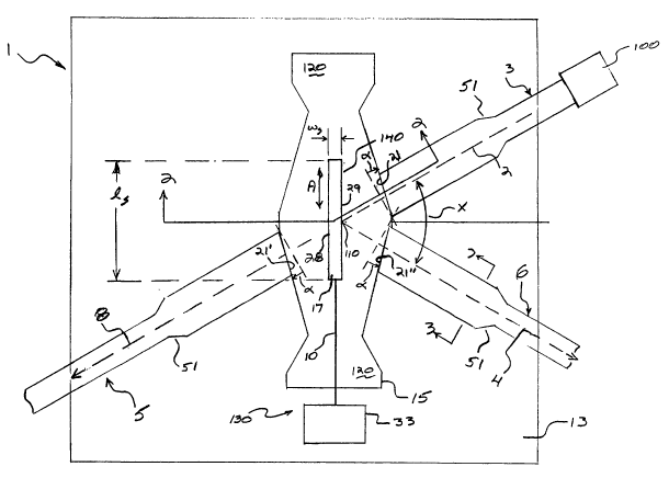
Referring now to the drawings in detail, and with initial reference to FIG. 1,
an optical
switch 1 constructed in accordance with an embodiment of the present invention
is there
depicted. The optical switch 1 of the present invention is preferably
constructed of silica-
based semiconductors (e.g., Si02), and other waveguides which weakly-confine
light. Other
semiconductors such as, for example, GaAs and InP, also might be used. In
addition, the
waveguide construction described below is provided as an illustrative, non-
limiting example
of an embodiment of the present invention; other waveguide geometries and
configurations
are contemplated by and fall within the scope and spirit of the present
invention.
While FIG. 1 depicts a 1 x 2 switch, it will be obvious to persons skilled in
the art and
from the disclosure herein that other configurations (e.g., 1 x N or M x N)
are contemplated
by and within the scope and spirit of the present invention. By way of
example, a 2 x 2
switch could be constructed by providing a second input waveguide opposite to
and having an
optical path coaxial with that of waveguide 6, as is discussed in greater
detail below in
connection with FIGS. 4A and 4B.
The switch 1 includes an input waveguide 3 and first and second output
waveguides 5,
6 arranged around and separated (input waveguide 3 and first output waveguide
S) by a trench
15. A cross-section of the second output waveguide 6, which is also exemplary
of the input
waveguide 3 and first output waveguide 5, is depicted in FIG. 3. The following
description of
and reference to the second output waveguide 6 shall also apply to the input
and first output
waveguides 3, 5. The waveguide 6 is constructed using semiconductor
fabrication techniques
and methods known to those skilled in the art, and thus need not be described
in detail here.
The waveguide 6 includes a core 7 deposited on a lower cladding layer 9b,
which is deposited
on a substrate 13. By way of non-limiting example, the substrate could be
silicon, quartz or
CA 02389597 2002-05-23
WO 01/38921 PCT/US00/32366
_7_
Si02. An upper cladding layer 9a is deposited over and around the core 7 to
form a buried
waveguide configuration.
The waveguides 3, 5, 6 may be formed from a wide variety of materials chosen
to
provide the desired optical properties. While it is preferable to construct
the optical switch 1
of the present invention on a silica-based (Si02) platform, other
semiconductors that provide
the desired optical properties may also be used. For example, the core 7 might
include
germanium-doped silica, while the upper and lower cladding 9a, 9b may include
thermal Si02
or boron phosphide-doped silica glass. This platform offer good coupling to
the fiber and a
wide variety of available index contrasts (0.35% to 1.10 %). Other platforms
which could be
used include, by way of non-limiting example, SiOXNY, polymers, or
combinations thereof.
Other systems such as indium phosphide or gallium arsenide also might be used.
With continued reference to FIG. 3, the core 7 can have an index of refraction
contrast
ranging from approximately 0.35 to 0.70%, and more preferably, the index of
refraction can
range from approximately 0.35 to 0.55% to allow for a high coupling to an
output fiber. The
core 7 can be rectangular, with sides running from approximately 3-10 p.m
thick and
approximately 3-15 ~.m wide. More preferably, the core 7 is square, with sides
from
approximately 6-8 pm thick and approximately 6-14 pm wide. The upper and lower
cladding
layers 9a, 9b adjacent to core 7 can be approximately 3-18 ~m thick, and are
preferably
approximately 15 ~m thick. and the core thickness can range from approximately
7 to 8 pm
for the same reason. In choosing the ultimate core and cladding dimensions,
care should be
taken to allow for low horizontal diffraction and good tolerance of
misaligrunents.
Again, these dimensions are offered by way of example and not limitation.
The present invention will work with both weakly-confined waveguides and
strongly-
confined waveguides. Presently, use with weakly-confined waveguides is
preferred.
Referring again to FIG. 1, the core 7 of input waveguide 3 defines an optical
path 2
along the waveguide's longitudinal length. That optical path 2 is generally
coaxial with an
optical path 8 defined by the core 7 of the first output waveguide 5. The
degree of non
CA 02389597 2002-05-23
WO 01/38921 PCT/US00/32366
_g_
coaxiality is determined on one side by the angle formed between the
perpendicular to the
propagation of the optical signal and the input waveguide-trench interface,
and on the other
side, by the trench length, as will be explained later. Thus, the input
waveguide 3 and first
output waveguide 5 may be considered to be arranged in registry with each
other with aligned
or coaxial optical paths, which maximizes the amount of light transferred from
input
waveguide 3 to first output waveguide 5.
The second output waveguide 6 also defines an optical path 4 that is oriented
with
respect to the input waveguide optical path 2 at a predetermined angle;
preferably between
approximately 30° and 80°. Thus, input waveguide optical path 2
intersects the second output
waveguide optical path 4 at an intersection point 110.
A trench 1 S is defined in the substrate 13 (see, e.g., FIGS. 2A and 2B) that
separates
the input waveguide 3 and first output waveguide 5, and around which the
waveguides are
arranged. The trench 15 is filled, partly or completely, with an optically
transparent medium
120 such as, for example, air, having an associated index of refraction n. For
air, the index of
refraction is approximately equal to 1.00.
By way of non-limiting example, the trench 15 could be approximately 8-40 ~m
wide,
and more preferably, 12-20 ~m wide.
A switching element 130 facilitates switching of an optical signal between the
input
waveguide 3 and one of the first and second output waveguides 5, 6. The
switching element
130 includes a shutter 17 provided in the trench 15 and an actuator 33 coupled
to the shutter
17 by a link 10 for providing selective movement of the shutter 17, as
described in more
detail below. Various embodiments of the actuator 33 are contemplated by the
present
invention including, by way of non-limiting example, electrothermal,
electrostatic, and
piezoelectric, each of which is described in more detail below.
The shutter 17 is preferably made from a light yet stiff material such as
silicon,
polymers, metallic or dielectric materials. Such a low-mass, rigid shutter 17
can be caused to
move quickly in response to an electrical signal, for example, between the
position depicted
CA 02389597 2002-05-23
WO 01/38921 PCT/US00/32366
-9-
in FIG. 1, in which the optical signal output from the input waveguide 3 is
reflected to the
second output waveguide 6, and a second position (not shown) in which shutter
17 is
displaced out of the light path so that an optical signal output from the
input waveguide 3
passes to the first output waveguide 5.
A highly-reflective coating is provided on at least one surface 140 of the
shutter 17,
preferably the surface facing the output facet 21 of the input waveguide 3.
Using gold fox that
coating provides a highly reflective face 29 at surface 140 which reflects the
light without
distortion (approximately 95% reflection) and is essentially wavelength
independent for
telecommunication, data communication, and spectroscopic applications, for
example. The
term "facet" refers to an end of a waveguide.
With continued reference to Fig. 1, the back 28 of shutter 140 could in like
manner be
coated with gold. Such coating would allow switch 7 to operate in the
alternate mode,
described above, whereby a 2 x 2 switch could be constructed by providing a
second input
waveguide (not shown) opposite to and having an optical path coaxial with that
of waveguide
6. In that structure light could be directed from the second waveguide by
reflection off the
back 28 of shutter 140 into output waveguide 5. The 2 x 2 switch is described
in greater
detail hereafter in connection with FIGS. 4A and 4B.
The shutter 140 can be from approximately 1-8 ~m thick, approximately 10-100
~m
high, and approximately 10-100 ~m long. The 140 shutter can be made from any
sufficiently
rigid and light material. Preferably, the shutter 140 is approximately 2 ~m
thick,
approximately 30-40 pm high, and approximately 30-40 p.m long. By way of non-
limiting
example, the shutter 140 is also preferably made from silicon, and the
reflective surfaces) 28,
29 can be made from gold.
With continued reference to FIG. 2A, the shutter 17 has a height hs sufficient
to
completely block and reflect light when the shutter 17 is in the second
position. It will be
appreciated that to block incoming optical signals completely, the shutter 17
should have a
height hs greater than the thickness t~ of core 7 and a length is greater than
the width w~ of
CA 02389597 2002-05-23
WO 01/38921 PCT/US00/32366
-10-
core 7. The length IS of the shutter 17 is preferably minimized to reduce the
distance required
for the shutter 17 to be moved from the first position to the second position,
which also
reduces the electrical power required to move the shutter 17 in and out of the
optical path and
improves the speed of the switch 1.
The width ws of the shutter 17 affects the insertion loss in the reflected
light path.
Specifically, a thinner shutter 17 may lower the insertion loss, with a
preferred dimension for
the shutter width being approximately 2 pm. The optical loss of the light
reflected off the
reflective surface 29 of the shutter 17, due to light diffraction in the
trench 15, can be
minimized by having the smallest possible minor thickness.
With continued reference to FIG. 1, the input waveguide 3 receives an optical
signal
(e.g., a WDM, DWDM, LTDWDM, etc.) from an optical source 100 (e.g., optical
fiber cable,
laser, etc.) and guides the optical signal in the core 7 and along an optical
path 2. The optical
signal exits the input waveguide 3 via an output facet 21 and enters the
trench 15. Depending
upon the position of the shutter 17, the optical signal will either propagate
across the trench
15 and enter the first output waveguide 5 via an input facet 21', or strike
and reflect off
coating 29 of face 140 (or, if no coating is provided, face 140 itself) and
propagate across a
part of the trench 15 and enter the second output waveguide 6 via an input
facet 21 ". In either
case, the optical signal will continue to propagate and be guided by the core
7 of the
respective waveguide along that waveguide's optical path.
With continued reference to FIG. 1, the actuator 33 of the switching element
130
controls the movement of the shutter 17 between the first and second
positions. Movement of
the shutter 17 may be in virtually any direction (e.g., along a plane parallel
with or
perpendicular to the bottom surface 150 of the trench 15), so long as that
movement provides
the ability to switch the optical signal between either of the output
waveguides 5, 6. For
example, FIGS. l and 2A depict a first embodiment of the switching element 130
having a
shutter 17 that is movable along a plane generally parallel with the plane of
the bottom
surface 150 of the trench 15 and in a direction generally indicated by arrow A
(FIG. 1 ).
CA 02389597 2002-05-23
WO 01/38921 PCT/US00/32366
-11-
Another embodiment is depicted in FIG. 2B in which the shutter 17 is movable
along
a plane generally perpendicular with the bottom surface 1 SO of the trench 15
and in a
direction generally indicated by arrow B. The movement direction of the
shutter 17 is not
critical, provided that the shutter 17 is movable into and out of the optical
path 2 defined by
S the input waveguide 3. When positioned in that optical path 2, the optical
signal will reflect
off the shutter 17 and be redirected into the second output waveguide 6. When
positioned out
of that optical path 2, the optical signal will traverse the trench 15 and
into the first output
waveguide 5. Movement of the shutter 17 by the actuator 133 may be in response
to a control
signal input to the actuator 133. That signal may be electrical, optical,
mechanical, or
virtually any other signal capable of causing the actuator to respond.
Turning now to FIGS. 4A and 4B, it will be appreciated that the reflective
shutter 117
is a very attractive switching element because both sides 128, 129 of the
shutter 117 could be
used for switching. This feature simplifies the construction of switch
matrices, since a
smaller number of shutters need be used to construct larger switches. In the
case of a 2 x 2
switch, for example, only one shutter 117 is needed to form a true 2 x 2 non-
blocking switch.
This is a remarkable improvement over other technologies, such as the use of a
thermo-
optical Mach-Zehnder Interferometer for a 2 x 2 non-blocking switch which
requires four
switching elements to achieve the 2 x 2 non-blocking switch.
With continued reference to FIGS. 4A and 4B, FIG. 4A depicts a 2 x 2 optical
switch
101 constructed in accordance with the present invention. The switch 101 is a
non-blocking
design, which means that a light signal present at any input may be directed
to any output
without affecting the ability to direct a light signal present at any other
input to any other
output. The switch 101 is depicted in more general view in FIG. 5, which shows
the
switching components, together with waveguides 103 and 112.
As depicted in FIG. 4A, switch 101 has a first waveguide 112 having an input G
and
an output Y. The waveguide 112 is non-continuous in that its optical path is
interrupted by a
trench 115 formed in a semiconductor substrate (not shown). A second waveguide
103 is
provided generally perpendicular to and intersecting the optical path of the
first waveguide
CA 02389597 2002-05-23
WO 01/38921 PCT/US00/32366
-12-
112 at the trench 115. The second waveguide 103 includes an input H and an
output Z. A
mirrored shutter 117 is selectively movable in and out of the trench 15 in
directions generally
indicated by arrow I. The mirrored shutter 117 has two generally parallel
surfaces 128, 129
that are highly reflective and that each act as a facet thus providing a dual-
facet mirror 117.
The mirrored shutter 117 may comprise a micro-mechanical shutter, or other
suitable device,
along the lines discussed previously in connection with other aspects of this
invention.
When the mirrored shutter 117 is positioned out of the trench 15 as depicted
in FIG.
4A, , the switch 101 is in an off state. An optical signal G' present at input
G of waveguide
112 will propagate therethrough and exit that waveguide 112 via output Y.
Likewise, an
optical signal H' present at input H of waveguide 103 will propagate
therethrough and exit
that waveguide 103 via output Z. Although the trench 15 interrupts the optical
path of each
waveguide 112, 103, the trench 15 does not otherwise affect light propagation
through the
waveguides 112, 103. When the mirrored shutter 117 is positioned in the trench
15 as
depicted in FIG. 4B, the switch 101 is in an on state, i.e., switching will
occur. A light signal
G' present at input G of waveguide 112 will contact the mirrored shutter 117,
reflect off
surface 128, and exit the switch 101 via output Z of waveguide 103. Similarly,
a light signal
H' present at input H of waveguide 103 will contact the mirrored shutter 117,
reflect off
surface 129, and exit the switch 101 via output Y of waveguide 112.
Turning now to FIG. 5, switch 101 is shown schematically, with first and
second
waveguides 112, 103, attached thereto.
FIG. 6 depicts a 4 x 4 switch 300 which employs six switches (also known as
switching elements) 301 of the type just described in connection with FIGS. 4A
and 4B
(known types of 4 x 4 switches such as free space MEMS switches and thermo-
optic Mach-
Zehnder interferometer switches require sixteen switching elements). This
switch 300 has
four input waveguides 303, 305, 307 and 309 into which are fed signals AA, BB,
CC, DD,
and four output waveguides, 311, 313, 315 and 317. Switches 301 can be set in
known
manner so that the signals AA, BB, CC and DD entering the switch 300 through
input
waveguides 303, 305, 307 and 309, respectively, are routed into output
waveguides 311, 313,
CA 02389597 2002-05-23
WO 01/38921 PCT/US00/32366
-13-
315 and 317 as desired. It will be appreciated that this invention reduces
significantly the
number of switching elements 301 which are required for the 4 x 4 switch 300.
Referring now to FIGS. 1 and 2B, actuator 33, 133 is joined to shutter 17 by
link 10,
110 and serves to shift the shutter 17 into and out of the optical path 2.
While any suitable
actuator could be used to implement the present invention, either an
electrothermal or
electromechanical type actuator is preferred.
Electrothermal actuators are generally known in the art, and therefore will
not be
described in precise detail. For the purposes of this invention, it will be
appreciated that any
electrothermal actuator could be used which sufficiently changes its size in
response to the
application of thermal energy (which, it will be appreciated, could be
generated by applied
electrical energy). One benefit to using electrothermal actuators is that such
actuators may be
latching-type devices, i.e., one that maintains its position without the
continuous application
of energy. Thus, a latching-type actuator will remain in either one of two
positions until it is
caused to switch out of that position.
An exemplary electrothermal latching-type actuator 233 suitable for use with
the
present invention is depicted in FIG. 7. That actuator 233 includes a flexible
member 34
which is securely fixed at endpoints 35, 35' to the walls of a cavity 37.
Cavity 37 is sized and
shaped to allow movement of flexible member 34 sufficient to cause the shutter
17 to move
between the first and second position. Also provided is a heater 39, which is
located in
relatively close proximity with the member 34. When the heater 39 is driven,
the member 34
warms and expands. Since the member's ends are secured at endpoints 35, 3~',
the member
34 cannot simply expand so that the endpoints shift outward. Instead,
compressive stresses
will be generated along the member's length. These stresses increase until
they reach a level
sufficient to cause the member 34 to change its position to that indicated by
reference
character D in FIG. 7. Thus, when the heater 39 is caused to heat (e.g., by
the application of
current through contacts (not shown)), the flexible member 34 also will be
warmed and
caused to move between an ambient position, indicated by reference character
C, and a flexed
CA 02389597 2002-05-23
WO 01/38921 PCT/US00/32366
-14-
position, indicated by reference character D. Alternatively, the member 34
could itself be the
heater.
An electrostatic actuator may also be used to selectively move shutter 17.
Benefits of
electrostatic actuators include high operating speed, low energy consumption,
and minimal
system heating. One type of electrostatic actuator 333 usable in connection
with the present
invention is depicted in FIG. 8 That actuator 333 includes electrodes 41, 41'
located on
opposite sides of a piezoelectric element 43 made from a material which
expands in at least
one dimension (i.e., width or length) when an electric field is applied to the
electrodes 41, 41'.
Piezoelectric element 43 may thus be caused to expand in the direction
indicated by arrow E,
imparting movement to the shutter 17.
It is possible that one actuator alone may not be sufficient to provide the
required
amount of movement for the shutter 17. This can be rectified by providing a
piezoelectric
actuator 433 having a number of interlaced fingers 45, such as that depicted
in FIG. 9. These
fingers are attached to a support 20 within actuator 433, which serves to
prevent unwanted
motion of one side of the fingers 45. When an electrical signal is applied to
electrodes (not
shown) of the actuator 433, the total displacement in the direction of arrow F
of endpoint 47
will reflect the cumulative displacement of all of the fingers 45. Since the
displacement of
endpoint 47 is the sum of the fingers' individual displacements, a significant
movement of the
shutter 17 can be achieved. This type of electrostatic actuator 433 may
require the application
of substantial voltage, possibly on the order of 100 V, to obtain the desired
movement of the
shutter 17. Despite the magnitude of this voltage potential, very little power
is required, since
the current flow through the electrostatic actuator 433 is negligible.
Referring again to FIG. 1, each of the waveguides 3, 5, 6 have an associated
index of
refraction determined, at least in part, by the material from which the
waveguide core 7 is
constructed. The associated index of refraction for the waveguides 3, 5, 6 are
approximately
equal to each other, and have a value of approximately 1.45 for the silica
platform. The
medium 120 provided in the trench 15 also has an associated index of
refraction that may be
different than the waveguide refractive indices. If the medium is air, for
example, its
CA 02389597 2002-05-23
WO 01/38921 PCT/US00/32366
-15-
refractive index is 1.00. When an optical signal experiences different
refractive indices as it
propagates, certain characteristics of that signal may be caused to change as
a result of the
different indices. For example, when an optical signal experiences different
refractive indices
as it propagates, part of the optical signal (in terms of optical power) may
be reflected back
into the input waveguide and along optical path 2. That reflected signal can
propagate back to
the source and cause it to destabilize.
Additionally, the optical signal may experience a phase shift when it passes
from a
material having a first refractive index to a material having a second and
different refractive
index. In some cases, that is the desired result. For an optical switch, it is
.preferable that the
optical signal not experience any significant change in its optical
characteristics as it is guided
along and switched by the various components that make up the switch.
To overcome the undesirable effects of the differing refractive indices, the
present
invention controls the distance between the output facet 21 of the input
waveguide 3 and the
input facets 21', 21" of the output waveguide 5, 6 so that the optical signal
propagates too
short a distance for the difference in refractive indices to introduce any
significant change in
the optical signal characteristics. Thus, even though the optical signal
completely traverses
the trench 15 (from input waveguide 3 to first output waveguide 5), or partly
traverses the
trench 15 (from input waveguide 3 to second output waveguide 6), the optical
signal does not
experience any significant adverse affect due to the difference in the medium
and waveguide
respective refractive indices.
Another aspect of the present invention compensates for optical return loss
(ORL)
caused when an optical signal passes between materials having different
refractive indices.
The difference in refractive indices may cause part of the optical signal (in
terms of optical
power) to be reflected and propagate back into the input waveguide and along
optical path 2,
for example. That reflected signal can disadvantageously reflect back to and
possible
destabilize the optical signal source. By angling the output facets 21, 21',
21" with respect to
the respective waveguide's optical path, (see, e.g., FIG. 1), any reflected
signal is directed
away from the waveguide core 7 and toward the cladding 9a or 9b, thereby
preventing the
CA 02389597 2002-05-23
WO 01/38921 PCT/US00/32366
-16-
reflected light from interfering with the optical signal being guided by and
propagating in the
input waveguide 3. In an embodiment of the present invention, the output
facets 21, 21', 21"
may be disposed at an angle a of about 5° to 10°, and more
preferably, about 6°-8° to
minimize the loss of light reflecting back into the input waveguide 3. For the
preferred case
of 6°, the shift against coaxiality mentioned earlier ranges from 0.2
pm for a 5.0 pm trench to
1.7 p.m for a 35 ~m trench.
In another aspect of the present invention, optical return loss may be further
minimized by applying an antireflective coating (not shown) to the waveguide
facets 21, 21',
21 ". The antireflective coating can be single layer or a multilayer
structure. Such a coating
can reduce reflection at the waveguide-trench interface from 3.5% to below 1 %
over a large
range of wavelengths. The materials and thickness forming the antireflection
coating layers
are identical to those used in thin film technology. For example, the best
single layer
antireflection coating layer between a silica waveguide and a trench at the
wavelength of 1.55
~,m has an refraction index of 1.204 and a thickness 322 nm.
In yet another embodiment, optical return losses may be minimized by using a
combination of an angled interface and an antireflection coating.
Another aspect of this invention relates to the shape of the waveguides 3, 5,
6 used to
direct light to and from the switch 1. According to this aspect of the
invention, and as shown
in FIGS. 1 and 10, a tapered neck region 51 is provided on at least one of the
waveguides 3, 5,
6 so that the waveguide width tapers to a smaller cross-section at a location
49 remote from
the trench 1 S. Tapered neck S 1 helps to reduce the diffraction of light in
the trench.
By way of non-limiting example only, in the region of the trench 15, the
waveguide
width may be in the range of approximately 5-15 pm. That width may taper to a
range of
approximately 4-10 ~m at the remote location 49. These dimensions, it will be
appreciated,
are by way of example, and other dimensions also might fall within the scope
and spirit of the
present invention.
CA 02389597 2002-05-23
WO 01/38921 PCT/US00/32366
-17-
Tapered neck region 51 provides a smooth transition as the optical signal
propagates
along and is guided by the waveguides 3, 5, 6. Tapered neck region5l confines
the light
traveling through the waveguide, in accordance with known principals of
waveguide optics,
and greatly reduces the transition loss which would otherwise occur where
light passes
between waveguides having different dimensions.
Various taper lengths and taper rates could be used, depending upon the
particular
considerations of a given installation.
The optical switch 1 of the present invention can be monolithically formed or
assembled using a flip-chip manufacturing technique, the latter being
generally depicted in
FIGS. 11A and 11B. In flip-chip manufacturing, the waveguides 3, 5 and 6 and
trench 15 are
monolithically formed on a first chip 200 using known semiconductor
fabrication techniques
and processes (e.g., deposition, etching, etc.), and the shutter 17 and
actuator 33 are formed
on a second chip 210. Prior to assembly, the two chips are oriented to face
each other, and
aligned so that corresponding parts (e.g., shutter 17 and trench 15) of the
chips oppose one
another. The chips are then joined.
Alternatively, in another embodiment of the present invention, the optical
switch 1
may be constructed by monolithically forming the switching element 130 and
waveguides 3,
5, 6. In such an embodiment, the various parts of the optical switch 1 are
formed on a single
substrate 13 through the selective deposition and removal of different layers
of material using
now known or hereafter developed semiconductor etching techniques and
processes. One of
the benefits of monolithic fabrication is that it avoids the need to register
the different
components before the two substrates are joined
Referring next to FIGS. 12A and 12B, both a flip-chip and monolithically
formed
optical switch 1 in accordance with the present invention are there
respectively depicted.
Both figures also depict connection of the optical switch 1 to external
optical components
such as, for example, optical fibers 67, such that waveguide cores 7 optically
connect with
fiber cores 65. Each optical fiber 67 is supported by a grooved member 69, and
secured in
place using a fiber lid 63. A glass cover 61 protects the underlying switch
components.
CA 02389597 2002-05-23
WO 01/38921 PCT/US00/32366
-18-
Alternative ways of securing the optical fibers, or of using other light
pathways, also could be
used.
One difference between the two fabrication techniques is the location of the
switching
element 130: above the waveguides for flip-chip and within the substrate 13
for monolithic.
It should be understood that this invention is not intended to be limited to
the angles,
materials, shapes or sizes portrayed herein, save to the extent that such
angles, materials,
shapes or sizes are so limited by the express language of the claims.
Thus, while there have been shown and described and pointed out novel features
of
the present invention as applied to preferred embodiments thereof, it will be
understood that
various omissions and substitutions and changes in the form and details of the
disclosed
invention may be made by those skilled in the art without departing from the
spirit of the
invention. It is the intention, therefore, to be limited only as indicated by
the scope of the
claims appended hereto.
It is also to be understood that the following claims are intended to cover
all of the
generic and specific features of the invention herein described and all
statements of the scope
of the invention which, as a matter of language, might be said to fall there
between. In
particular, this invention should not be construed as being limited to the
dimensions,
proportions or arrangements disclosed herein.