Note: Descriptions are shown in the official language in which they were submitted.
CA 02389980 2002-05-02
WO 01/33711 PCT/CA00/00583
TIME BASE COMPRISING AN INTEGRATED
MICROMECHANICAL RING RESONATOR
The present invention relates to a time base, i.e. a device comprising a
resonator and an integrated electronic circuit for driving the resonator into
oscillation
and for producing, in response to this oscillation, a signal having a
determined
frequency.
Time bases, or frequency standards, are required in a large variety of
electronic devices, ranging from wristwatches and other timepieces to complex
telecommunication devices. Such time bases are typically formed by an
oscillator
including a quartz resonator and an electronic circuit for driving the
resonator into
oscillation. An additional division chain may be used to divide the frequency
of the
signal produced by the oscillator in order to obtain a lower frequency. Other
parts of
the circuit may serve to adjust the frequency, for example by adjusting the
division
ratio of the division chain. The components of the electronic circuit are
advantageously integrated onto a single semiconductor substrate in CMOS
technology. Other functions, not directly related to the frequency processing,
may be
integrated onto the same substrate.
Advantages of quartz resonators are their high quality factor Q leading to
good
frequency stability and low power consumption as well as their good
temperature
stability. A disadvantage of typical time bases using quartz resonators
however
resides in the fact that two components, namely the quartz resonator and the
integrated electronic circuit, are required in order to provide a high-
precision
frequency. A discrete quartz resonator requires board space which is scarce in
many
cases. For instance, a standard quartz resonator for wristwatch applications
requires
space of the order of 2x2x6 mm3. Moreover, additional costs are caused by the
assembly and connection of the two components. Yet, space and assembly costs
are
major issues, especially in the growing field of portable electronic devices.
It is thus a principal object of the present invention to provide a solution
to the
above-mentioned problems by providing a time base comprising an integrated
resonator.
Another object of the present invention is to provide a time base that may be
fully integrated on a single substrate, that is suitable for mass production
and that is
compatible with CMOS technology.
Still another object of the present invention is to provide a time base
comprising a resonator having an improved quality factor O and thereby a
greater
frequency stability and low power consumption.
COPIE DE CONFIRMATfON
CA 02389980 2002-05-02
WO 01/33711 PCT/CH00/00583
-2-
Yet another object of the present invention is to provide such a time base
which is low-priced and requires only a very small surface area on a
semiconductor
chip.
Accordingly, there is provided a time base comprising a resonator and an
integrated electronic circuit for driving said resonator into oscillation and
for producing,
in response to said oscillation, a signal having a determined frequency,
characterised
in that said resonator is an integrated micromechanical ring resonator
supported
above a substrate and adapted to oscillate, according to a first oscillation
mode,
around an axis of rotation substantially perpendicular to said substrate, said
ring
resonator comprising
- a central post extending from said substrate along said axis of rotation;
- a free-standing oscillating structure connected to said central post and
including
- an outer ring coaxial with said axis of rotation; and
- a plurality of spring elements disposed symmetrically around said central
post
and connecting said outer ring to said central post;
and
- at least one pair of diametrically opposed electrode structures disposed
around said outer ring and connected to said integrated electronic circuit.
An advantage of the time base according to the present invention lies in the
fact that the micromechanical ring resonator exhibits a high quality factor Q.
Quality
factors as high as 2x10⁵ have been measured. For comparison, tuning-fork
quartz
resonators usually exhibit values between 5x10⁴ and 1 x10⁵ after laser
trimming of the
fork tines. Different design features favouring a high quality factor Q are
the object of
dependent claims and will be described hereinafter in detail.
In addition, for a given resonant frequency, the surface area required on the
substrate to form the ring resonator is small in comparison with other
resonators.
According to one aspect of the invention, the electronic circuit is
advantageously integrated on the substrate together with the micromechanical
ring
resonator, thereby leading to a low-priced time base. A lower price is also
obtained by
wafer-level packaging of the resonator using wafer-bonding technology.
It must be pointed out that ring resonators having similar features are known
from sensing devices, such as angular rate sensors, accelerometers or
gyroscopes.
For instance U.S. Patent No. 5,450,751 to Putty et al. and U.S. Patent No.
5,547,093
to Sparks both disclose a micromechanical ring resonator for a vibratory
gyroscope
comprising a plated metal ring and spring system supported above a silicon
substrate.
U.S. Patent No. 5,872,313 to Zarabadi et al. discloses a variant of the above
sensor
CA 02389980 2002-05-02
WO 01/33711 PCT/CH00/00583
-3-
which is configured to exhibit minimum sensitivity to temperature variation.
U.S. Patent
No. 5,025,346 also discloses a ring resonator for use as a micro-sensor in a
gyroscope or an angular rate sensor.
None of the above-cited documents however indicates or suggests using such
a type of ring resonator in an oscillator circuit to act as a frequency
standard or time
base. Moreover, a number of design features (e.g. the shape and number of
spring
elements) of the ring resonators disclosed in these documents are such that
they
would not be suitable for horological applications where frequency stability
and low
power consumption are essential. For instance, the resonating structures
disclosed in
U.S. Patent No. 5,025,346 exhibit a quality factor ranging from 20 to 140
which is too
low for being used in a highly precise time base in horological applications,
whereas
quartz resonators used in horological applications exhibit quality factors of
the order of
1 x10⁴ to 1 x10⁵.
According to the present invention, various design features are proposed which
lead to a high quality factor Q, a high stability of the oscillation frequency
against
variations in the amplitude of the driving voltage, and tolerance of
fabrication process
variations. In fact, one of the major objectives for an application as an
oscillator is a
high quality factor Q. A high quality factor Q results in a stable oscillation
with low
phase noise and low power consumption, as is required for horological
applications.
According to other aspects of the present invention, various mechanisms are
proposed for substantially compensating for the effect of temperature on the
resonant
frequency of the ring resonator.
According to another aspect of the present invention, a temperature measuring
circuit may further be integrated on the substrate in order to compensate for
the effect
of temperature on the frequency of the signal produced by the time base. Such
compensation of the resonator's temperature dependency may easily be effected
since the ring resonator of the present invention has the advantage of
exhibiting
substantially linear temperature characteristics.
According to still another aspect of the present invention, a second
micromechanical ring resonator may be formed on the substrate in order to
allow
temperature compensation. According to another aspect of the invention,
temperature
compensation is also achieved by using a single micromechanical ring resonator
which is operated simultaneously with two oscillation modes having different
resonant
frequencies.
Other aspects, features and advantages of the present invention will be
apparent upon reading the following detailed description of non-limiting
examples and
embodiments made with reference to the accompanying drawings, in which
CA 02389980 2002-05-02
WO 01/33711 PCT/CH00/00583
-4-
- Figure 1 is a top view illustrating schematically a first embodiment of a
time
base according to the present invention comprising a micromechanical ring
resonator
and an integrated electronic circuit;
- Figure 2 is a detailed view of the central post of the micromechanical ring
resonator and its junctions with the spring elements;
- Figure 3 is a detailed view of a portion of the outer ring with its
junctions with
the spring elements;
- Figure 4 is a cross-sectional view of the micromechanical ring resonator of
Figure 1 taken along line A-A';
- Figure 5 shows an idealized straight spring element with a section of the
outer ring;
- Figure 6 shows a top view illustrating schematically a second embodiment of
a time base according to the present invention;
- Figures 7a to 7c show detailed top views of three different designs intended
to prevent the ring resonator from sticking on the electrode structures;
Figure 8 shows a top view illustrating an improvement of the first embodiment
shown in Figure 1;
- Figure 9 is a cross-sectional view of the embodiment of Figure 8 taken along
line A-A';
- Figures 10a and 10b are two top views illustrating two variants of a
mechanism for altering the mass moment of inertia of the ring resonator as a
function
of temperature, in order to substantially compensate for the effect of
temperature on
the resonant frequency of the ring resonator;
- Figures 11 a and 11 b are respectively top and cross-sectional views
illustrating a second mode of oscillation where the resonator performs a
tilting
oscillation; and
- Figures 12a and 12b are respectively top and cross-sectional views
illustrating another second mode of oscillation where the resonator performs a
vertical
oscillation perpendicular to the substrate plane.
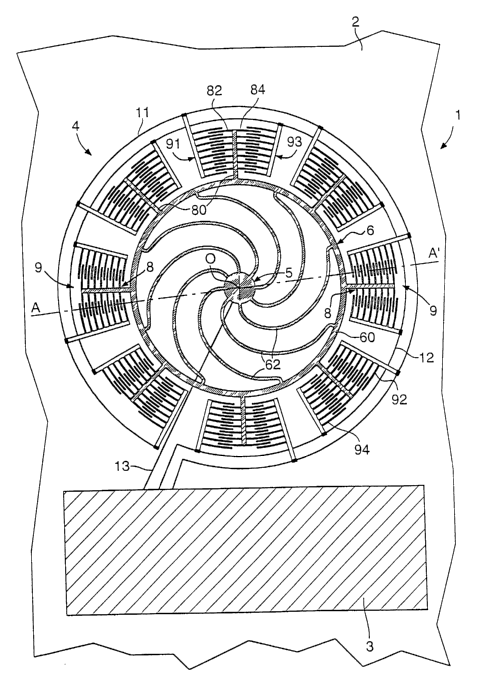
Figure 1 schematically shows a top view of a first embodiment of the present
invention. There is shown an integrated time base, indicated generally by
reference
numeral 1, comprising a resonator 4 and an integrated electronic circuit 3 for
driving
the resonator into oscillation and for producing, in response to this
oscillation, a signal
having a determined frequency. Figure 4 shows a cross-sectional view of the
ring
resonator 4 taken along line A-A' as shown in Figure 1.
The integrated electronic circuit 3 is not shown in detail since this circuit
may
easily be designed by those skilled in the art. Preferably both the integrated
electronic
CA 02389980 2002-05-02
WO 01/33711 PCT/CH00/00583
-5-
circuit 3 and the resonator 4 are realized and integrated on a same substrate
2 as
illustrated in Figure 1. A preferred substrate material is silicon, but other
similar
materials known by those skilled in the art to be equally suitable for
realising the time
base of the present invention may be used.
According to the present invention, the resonator 4 is realised in the form of
a
monolithic micromechanical resonating ring, hereinafter referred to as a
micromechanical ring resonator, which is essentially supported above the
substrate 2
and adapted to oscillate around an axis of rotation O substantially
perpendicular to the
substrate 2. The ring resonator 4 essentially comprises a central post 5
extending
from the substrate 2 along the axis of rotation O and a free-standing
oscillating
structure, indicated globally by reference numeral 6, connected to the central
post 5.
The free-standing oscillating structure 6 includes an outer ring 60 coaxial
with
the axis of rotation O, and a plurality of spring elements 62 disposed
symmetrically
around the central post 5 and connecting the outer ring 60 to the central post
5. The
spring elements 62 are essentially formed as curved rod-shaped spring
elements. It
will be appreciated that the central post 5 constitutes the only mechanical
connection
of the ring resonator 4 with the substrate 2 and that oscillation of the
resonator takes
place in a plane substantially parallel to the surface of the substrate 2.
The ring resonator 4 according to the present invention further comprises
pairs
of diametrically opposed electrode structures surrounding the outer ring 60,
indicated
by reference numeral 9 in Figure 1. According to this first embodiment, comb-
shaped
members 8 are provided on the outer ring 60 of the free-standing oscillating
structure
6. These comb-shaped members 8 form a part of the electrode structures of the
ring
and each include a base member 80 extending radially from the outer ring 60
and first
and second lateral members, indicated respectively by reference numerals 82
and 84,
that extend substantially perpendicularly from both sides of the base member
80.
The electrode structures 9 comprise first and second comb-shaped electrode
structures 91 and 93 surrounding the outer ring 60 in such a way that they
mesh with
the comb-shaped members 8 of the free-standing oscillating structures. More
particularly, according to this embodiment, the first comb-shaped electrode
structure
91 includes first electrodes 92 and meshes with comb-shaped member 8 so that
the
first electrodes 92 are adjacent to the first lateral members 82. Similarly,
the second
comb-shaped electrode structure 93 (disposed opposite the first comb-shaped
electrode structure 91 ) includes second electrodes 94 and meshes with comb-
shaped
member 8 so that the second electrodes 94 are adjacent to the second lateral
members 84. As shown in Figure 1, the lateral members 82, 84 and the
electrodes 92,
94 of the first and second electrode structures 91, 93 are preferably designed
so as to
CA 02389980 2002-05-02
WO 01/33711 PCT/CH00/00583
-6-
have the shape of an arc of a circle concentric with the outer ring 60.
In this embodiment, the first comb-shaped electrode structures 91 serve to
electrostatically drive the ring resonator 4 into oscillation, and the second
comb-
shaped electrode structure 93, which are disposed on the other side of the
base
members 80, serve to capacitively sense the oscillation of the resonator. The
first
electrode structures 91 surrounding the resonator 4 are connected together via
a first
conductor 11 formed on the substrate 2, and, similarly, the second electrode
structures 93 are connected together via a second conductor 12 formed on the
substrate 2. These conductors 11, 12 as well as a third conductor 13 providing
an
electrical contact to the ring via the central post 5 are connected to
appropriate
terminals of the electronic circuit 3.
Figure 4 shows a cross-sectional view of the ring resonator 4 taken along line
A-A' as illustrated in Figure 1. Thickness and other dimensions are not to
scale. There
is shown the substrate 2, the central post 5 along the axis of rotation O of
the ring
resonator, the free-standing oscillating structure 6 including the outer ring
60 and the
spring elements 62, the lateral members 82 of the comb-shaped members 8, the
electrodes 92 of the first comb-shaped electrode structures 91, and the first
and
second connectors 11, 12 that respectively connect the electrode structures 91
and 93
surrounding the outer ring 60. Figure 4 further shows a first insulating layer
20, such
as a silicon oxide layer, formed above the surface of substrate 2, beneath the
ring
resonator 4 and onto which are formed the first and second conductors 11, 12.
A
second insulating layer 21, such as another oxide layer or silicon nitride
layer, is
formed above the first layer 20 below the ring resonator.
The resonating ring structure is preferably manufactured by means of silicon
surface micro-machining techniques which are familiar to those skilled in the
art and
will therefore not be described here. One such technique makes use of a poly-
silicon
layer deposited on top of a so-called "sacrificial layer" in order to form the
free-
standing structures of the resonator. Another technique uses a buried oxide
layer,
such as e.g. in a silicon on insulator (S01) wafer, as the sacrificial layer
and results in
a free-standing structure made of mono-crystalline silicon. Other material and
processing techniques, however, may also be used to realise the
micromechanical
ring resonator according to the present invention.
One of the major objectives for an application as a time base or frequency
standard is a high quality factor Q of the resonator. A high quality factor Q
results in a
stable oscillation with low phase noise and low power consumption as is
required for
horological applications. The quality factor Q of the micromechanical ring
resonator
according to the present invention is very high due to a number of
advantageous
CA 02389980 2002-05-02
WO 01/33711 PCT/CH00/00583
_7_
design features that will be explained below. As already mentioned
hereinabove,
quality factors as high as 2x10⁵ have been measured on these structures. For
comparison, tuning-fork quartz resonators usually exhibit values between 5x10⁴
and
1 x10⁵ after laser trimming of the fork tines.
The shape of the spring elements 62 connecting the outer ring 60 to the
central post 5 is optimised so as to obtain a high quality factor Q. In
contrast to the
conditions present when using straight spring elements, the tensions along the
bending line are, in the present case, homogeneously distributed along the
spring
element. The curved shape is such that energy losses per oscillation period
are kept
minimal.
In addition, junctions 63 of the spring elements 62 with the central post 5
are
substantially perpendicular, as shown in Figure 2. Preferably, round shapes or
fillets
63a are provided at the junctions 63. These fillets 63a prevent notch tensions
during
oscillation, thereby favouring an elevated quality factor Q, as substantially
no energy
is dissipated in the central post 5 during oscillation. Furthermore, the
central post 5
remains substantially free of tension, which again favours a high quality
factor Q.
Figure 3 shows the junctions 64 of the spring elements 62 with outer ring 60.
Here
also, substantially perpendicular junctions 64 and fillets 64a are preferred
designs.
Using a plurality of spring elements 62 rather than the minimum of three
required for a well-defined suspension increases the quality factor Q. Due to
the fact
that minor geometrical variations (e.g. as a result of spatial fluctuations in
processing)
as well as material inhomogeneities are averaged over the plurality of spring
elements, the quality factor Q increases with the number of spring elements.
The
upper limit is given by geometrical restrictions due to the design rules of
the micro-
structuring process. The number of spring elements is therefore comprised
between
four and fifty, and preferably is of the order of twenty.
Another element favouring a high quality factor Q of the ring resonator is the
perfect rotationally symmetrical structure, where the centre of gravity of the
entire
structure remains motionless. Non-linear effects, present in most other
resonator
designs, are thereby removed to a large extent.
The resonant frequency of the ring resonator can be adjusted over a wide
range by changing the geometrical dimensions of the device. The ring resonator
can
be looked at as a plurality of spring elements connected to a segment of the
outer
ring. In a zero-order approximation, and in order to obtain a close algebraic
expression for the resonant frequency, one can study the case of a straight
spring
element 22 with a segment 27 of the outer ring 60, as shown in Figure 5. The
resonant frequency f,. of this structure reads
CA 02389980 2002-05-02
WO 01/33711 PCT/CH00/00583
_g_
N 1 3~E~J
r 2n
13(mr +0.24~ms)
where J = d ~ w3 / 12 is the surface moment of inertia of the structure, E is
the
elasticity module, d, w and I are the thickness, width and length of the
straight spring
element 22, respectively, and m~, ms are the masses of the ring segment 27 and
spring element 22, respectively. It can be easily seen from the above formula,
that the
resonance frequency can be influenced by varying the width and/or length of
the
spring elements or by varying the mass of the outer ring (including the mass
of the
comb-shaped members 8), again via its geometrical dimensions. Scaling of the
entire
structure further widens the accessible frequency range.
It is important for mass production of such ring resonators to keep the
resonant
frequency from one chip to the other within small tolerances. Tolerances in
the
resonant frequency due to slight variations in process parameters can be
greatly
reduced by carefully dimensioning the ring and springs. This can again be
shown
using the example of Figure 5. The resonant frequency will be lower than the
projected frequency if the width of the spring elements 22, indicated by
reference
numeral 26, is smaller after processing, e.g. due to an over-etch, than a
desired width
25. However, if one considers that at the same time the mass of the ring 60
(as well
as the mass of the base members 80 and lateral members 82, 84) is lowered due
to
the same over-etch, the decrease of the resonant frequency will be compensated
for
by the reduction of the masses. Openings in the ring and the bars (not shown
in the
Figures), which may be necessary for processing the structure, favour this
effect.
The surface area required by the micromechanical ring resonator according to
the present invention is very small with respect to the resonant frequency
obtained.
For instance, a ring resonator according to the present invention designed for
a rather
low frequency of 32 kHz requires a surface of well below 1 mm2. Conventional
structures require relatively large structures in order to obtain such a low
frequency.
For a given geometrical layout, the dimensions and frequency are inversely
related,
i.e. the larger the geometrical dimensions, the lower the frequency. Far
comparison,
EP 0 795 953 describes a silicon resonator requiring a surface of about 1.9
mm2 for a
higher frequency of 1 MHz. It is obvious that the substrate surface area
required by
the resonator is directly related to the price of the integrated time base.
The resonant frequency of the ring resonator is, within the temperature range
of 0 to 60°C, in good approximation, a linear function of temperature.
At a resonant
frequency of 45 kHz, it has been observed that the thermal coefficient of the
resonant
CA 02389980 2002-05-02
WO 01/33711 PCT/CH00/00583
_g_
frequency is of the order of -25 ppm/°C: It is thus desirable to
incorporate, in the
same substrate 2, a temperature measuring circuit having an output signal
which may
be used to compensate for the frequency variation by adequately adjusting the
frequency of the signal produced by the time base.
To this effect, the time base according to the present invention may
advantageously comprise an integrated temperature measuring circuit (not
shown).
An example of such a temperature measuring circuit is described in the article
"Smart
Temperature Sensor in CMOS Technology" by P. Krumenacher and H. Oguey, in
"Sensors and Actuators", A21-A23 (1990), pages 636 to 638. Here, temperature
compensation is achieved by acting on the division ratio of the division
chain, for
instance using an inhibition technique well known to those skilled in the art.
Alternatively, two ring resonators with different resonant frequencies may be
integrated onto the same chip, such arrangement allowing the chip temperature
to be
precisely determined by measuring the frequency difference of the two
resonators
(both ring resonators have the same temperature coefficient since they are
made from
the same material).
The advantage of using integrated time bases according to the present
invention is twofold: Firstly, the temperature dependency of the ring
resonator is linear
which facilitates the electronic signal treatment necessary to compensate for
the
temperature. Secondly and more importantly, the small size and monolithic
integration
of the ring resonator allows a second resonator to be provided with only a
slight
increase in chip size and without further external connections.
Alternatively, according to a particularly advantageous embodiment of the
invention, it is possible to use a single ring resonator which operates
simultaneously
with two oscillation modes. A first of these modes is the above described
rotational
mode. A second oscillation mode may be a tilting oscillation mode, wherein the
free-
standing structure 6 performs a tilting oscillation against the substrate
plane. This
tilting oscillation mode may be excited electrostatically and sensed
capacitively by
using further electrodes on the substrate under the ring area. The two modes
are
selected to have different frequencies so that temperature compensation may be
achieved by measuring the frequency difference. A schematic illustration of
the above
mentioned tilt mode is shown in Figures 11a and 11b. As shown in these
figures, two
sets of electrodes 100 and 120 (in this case four) having substantially the
shape of
arcs of circles are disposed on the substrate under the ring 60 so that the
first set of
electrodes 100 drives the structure 6 into a tilting oscillation and the
second set of
electrodes 120 senses this tilting oscillation. The set of driving electrodes
100 and the
set of sensing electrodes 120 are disposed on opposite sides of the structure
6 with
CA 02389980 2002-05-02
WO 01/33711 PCT/CH00/00583
-10-
respect to the central post 5 (respectively on the left and right sides in
Figure 11 a).
A second oscillation mode may be a vertical oscillation mode, wherein the free-
standing structure 6 performs a vertical oscillation perpendicular to the
substrate
plane, i.e. the free-standing structure 6 oscillates in a direction parallel
to the axis of
rotation O. A schematic illustration of the above mentioned perpendicular mode
is
shown in Figures 12a and 12b. As shown in these figures, two sets of
electrodes 130
and 150 are disposed on the substrate under the ring 60 so that the first set
of
electrodes 130 drives the structures 6 into an oscillation perpendicular to
the substrate
plane and the second set of electrodes 150 senses this oscillation. In
contrast to the
tilting mode, the set of driving and sensing electrodes 130, 150 are disposed
symmetrically around the central post 5, i.e. the sets of electrodes each
comprise
diametrically opposed electrodes.
As already mentioned, the comb-shaped electrode structures 91 shown in the
embodiment of Figure 1 serve to electrostatically drive the ring resonator
into
oscillation and the opposite comb-shaped electrode structures 93 serve to
capacitively
sense this mechanical oscillation. An alternating voltage signal is applied to
electrode
structures 91 resulting in electrostatic forces on the ring and oscillation
thereof, which,
in turn, induces an alternating signal on the opposite set of electrode
structures 93,
when the resonator operates. It will be understood that electrode structures
91 and 93
are interchangeable.
Since there is a parabolic relationship between the voltage applied on the
electrodes and the resulting force on the ring and, it is desirable to add a
constant
direct voltage to the alternating voltage so as to obtain a substantially
linear force-
voltage relationship. In the schematic representation of Figure 1, there are
shown
three signal lines or conductors 11 to 13 that are respectively connected to
electrode
structures 91, electrode structures 93 and central post 5. These lines serve
to drive
the ring resonator into oscillation and to sense this oscillation via the
respective
electrode structures.
According to a first variant, conductor 13 may be used to apply the direct
voltage component to the ring resonator via the central post 5, while the
alternating
voltage component is applied to electrode structures 91 via conductor 11,
conductor
12 being used to sense the resulting signal. According to a second variant,
the
alternating driving voltage and the direct voltage component may be superposed
on
electrode structures 91 via conductor 11 while the ring resonator is tied to a
fixed
potential, such as e.g. ground, via conductor 13. Conductor 12 is used to
sense the
signal in this case. It will be appreciated that electrode structures 91 and
93 are
interchangeable and that electrode structures 93 may alternatively be used for
driving,
CA 02389980 2002-05-02
WO 01/33711 PCT/CH00/00583
-11-
electrode structures 91 being used for sensing.
Alternatively, sensing may be done by detecting a change in impedance at
resonance. As represented in Figure 6, such a solution requires only two
conductors,
11 and 13, and an electrode structure 9* comprising a single set of comb-
shaped
electrode structures 91 connected to conductor 11 (the comb-shaped members 8*
are
modified accordingly and only comprise first lateral members 82). According to
a first
variant, the alternating driving voltage is applied, via conductor 11, to the
single set of
electrode structures 91, and the direct voltage component is applied to the
ring via
conductor 13. According to another variant, the sum of alternating and direct
driving
voltages can be applied to electrode structures 91 via conductor 11, the ring
being in
this case tied via conductor 13 to a fixed potential such as e.g. ground.
The two-conductor option provides two advantages, namely (i) a reduction in
the diameter of the entire structure since a second conductor and a second set
of
electrode structures surrounding the ring is no longer required, and (ii) the
possibility
of providing a larger number of comb-shaped electrode structures 91 along the
periphery of the outer ring 60, resulting in an enhanced signal.
The different modes of operation of the ring resonator are summarized in the
following table. It will be appreciated that, in any of the above-mentioned
variants, the
signals applied to the driving electrodes and the ring, namely the alternating
driving
voltage and the direct voltage component, are perfectly interchangeable.
Electrodes Rin Electrodes Remarks
91 93
3 ConductorsAC-drivin DC-bias Sensin Electrodes
91
AC-driving Fixed potential,Sensing and 93 are
+ e. . round interchangeable
DC bias
DC-bias AC-drivin Sensin
Fixed potential,AC-driving Sensing
e. . round +
DC-bias
2 ConductorsAC-drivin DC-bias Sensing is
done
AC-driving Fixed potential, by detecting
+ e. . round a
DC bias change in
DC-bias AC-drivin impedance
at
Fixed potential,AC-driving resonance
e. . round +
DC-bias
The fact that the lateral members 82, 84 and the electrodes 92, 94 are of
CA 02389980 2002-05-02
WO 01/33711 PCT/CH00/00583
-12-
curved shape and concentric with outer ring 60 reduces non-linearities in the
electro-
mechanical coupling, resulting in a high quality factor Q on the one hand and
a
resonant frequency of the ring resonator which is essentially independent of
the
amplitude of alternating and direct driving voltages on the other hand.
Furthermore,
the micromechanical ring resonator according to the present invention can be
driven
with voltages as low as 1.5 V, which is a major advantage for portable
electronic
applications.
In addition, due to electrostatic driving and capacitive sensing, and due to
the
high quality factor Q determined by the design, the power consumption of the
ring
resonator is ten to hundred times lower than that of a quartz, which is of
particular
interest for portable electronics applications.
Figures 7a to 7c show three different advantageous design features intended
to prevent the ring resonator from sticking in case of a shock. According to a
first
variant shown in Figure 7a, stop structures 28 disposed on the substrate 2 are
provided at outer ends 80a of the base members 80. These stop structures 28
are
designed so as to limit the angular movement of the ring structure 6 and
therefore
prevent the free-standing oscillating structure 6 from sticking on the
electrode
structures 9 when excessive angular movements take place due, for instance, to
mechanical shocks.
Alternatively, as shown in Figure 7b, extremities 82a, 84a of the lateral
members 82, 84 and/or extremities 92a, 94a of the electrodes 92, 94 may be
designed so as to exhibit a pointed shape or at least a suitably small surface
area so
as to prevent sticking.
Finally, as shown in the variant of Figure 7c, one 82*, 84* of the lateral
members 82, 84 can be made longer than the others, thereby reducing the
adhesion
forces when the comb-shaped members 8 and the comb-shaped electrode structures
91, 93 get into mechanical contact with each other. Obviously, the same effect
may be
obtained when one of electrodes 92 and 94 is longer than the others.
Figures 8 and 9 show an improvement of the micromechanical ring resonator 4
according to the present invention which is illustrated in Figure 1. Figure 9
shows a
cross-sectional view of Figure 8 taken along line A-A'. A conductive pattern
31 is
provided on (or below) the surface of the substrate 2 under at least part of
the free-
standing oscillating structure 6, i.e. spring elements 62, outer ring 60, as
well as
comb-shaped members 8, the shape of this conductive pattern 31 being
essentially a
projection of the free-standing oscillating structure 6 on the surface of the
substrate 2.
Connecting this conductive pattern 31 to the same potential as the free-
standing
oscillating structure 6 suppresses forces perpendicular to the substrate 2
between the
CA 02389980 2002-05-02
WO 01/33711 PCT/CH00/00583
-13-
ring resonator 4 and the surface of the substrate 2 leading to a resonant
frequency
which is independent of the direct voltage component.
Figures 10a and 10b show further improvements of the micromechanical ring
resonator 4 according to the present invention which allow the temperature
coefficient
of the resonant frequency to be reduced to a value close to zero. Two main
factors
determine the temperature characteristics of the ring resonator. Firstly,
Young's
modulus E of the material used to realize the vibrating structure decreases
With
increasing temperature resulting in a reduced stiffness of the spring elements
62 and
therefore a lower resonant frequency. Secondly, due to thermal expansion, the
diameter of the ring will increase with increasing temperature resulting in an
increased
mass moment of inertia of the structure, which, in turn, also reduces the
resonant
frequency.
Different thermal expansion coefficients of different materials can be used to
introduce a compensation mechanism 65, as sketched in Figure 10a or 10b. As
shown in Figures 10a and 10b, a plurality of thermally compensating members 65
(only one is shown in the Figures) are attached to the outer ring 60. These
thermally
compensating members 65 are designed to alter the mass moment of inertia of
the
free-standing oscillating structure 6 as a function of temperature so as to
substantially
compensate for the effect of temperature on the resonant frequency of the
resonator
4. To this effect, the members 65 include a weight member 66 connected to the
outer
ring 60 by means of a connecting member 67 comprising first and second layers
68,
69 made respectively of first and second materials having different thermal
coefficients. The materials are chosen so that the thermal expansion
coefficient atn~
of the first layer 68 is smaller than the thermal expansion coefficient atn2
of the
second layer 69. In a preferred embodiment, the first material is silicon and
the
second material is a metal, preferably aluminium.
The design of the mechanism 65 according to Figure 10a is such that, with
increasing temperature, the connecting member 67 straightens due to the
different
thermal expansion of the first and second layers 68, 69. As a consequence, the
weight
members 66 move towards the centre of the ring, i.e. closer to the axis of
rotation O of
the oscillating structure 6, thereby reducing the mass moment of inertia of
the ring
resonator, resulting in an increase of the resonant frequency which
substantially
counteracts the effect of the Young's modulus and the thermal expansion of the
ring
on the resonant frequency. Such thermal compensation mechanisms can
alternatively
be attached to the outer side of the ring 60, as shown in Figure 10b, or to
some other
part of the free-standing oscillating structure 6 so as to alter its mass
moment of
inertia as a function of temperature. The layout and fabrication of the
members 65
CA 02389980 2002-05-02
WO 01/33711 PCT/CH00/00583
-14-
have to be realized so that the weight members 66 move towards the axis of
rotation
O of the ring resonator when temperature increases.
Having described the invention with regard to certain specific embodiments, it
is to be understood that these embodiments are not meant as limitations of the
invention. Indeed, various modifications and/or adaptations may become
apparent to
those skilled in the art without departing from the scope of the annexed
claims.