Note: Descriptions are shown in the official language in which they were submitted.
s
CA 02390243 2002-07-11
BUCK REGULATOR CIRCUIT FOR USE IN A POWER SUPPLY
FIELD OF THE INVENTION
The present invention relates generally to regulator/converter circuits for
use in power supplies and more specifically, to a buck regulator/converter
circuit
that is capable of providing at least two different output voltage levels.
BACKGROUND OF THE INVENTION
A large number of machinery use DC voltage for operation. The DC
voltage may be supplied either by a battery or by an AC power source that has
been stepped down by a transformer and rectified by a diode bridge. Because
voltage from a battery or rectifier bridge is fixed and unregulated, many
systems
also include a DC-to-DC regulatorlconverter intermediate between the power
source and the rest of the machinery. The DC-to-DC regulator/converter
regulates/converts the unregulated power from the battery or rectifier bridge
into a
regulated DC power source for use by the machinery. The DC-to-DC
regulator/converter may also decrease or increase the voltage output by the DC-
to-
DC converter.
As an example, many welding and cutting systems use an AC voltage
source for power. The AC voltage source is rectified and provided to a DC-to-
DC
regulator/converter. The DC-to-DC regulator/converter regulates the voltage
and
provides a controlled output DC voltage for use in the welding or cutting
system to
initiate and maintain the welding or cutting process.
A common DC-to-DC regulator/converter used in the industry is referred to
as a "buck" regulator. A buck regulator typically not only regulates the
ripple in
the DC output, but it also steps down the DC output voltage level from that of
the
voltage input into the buck regulator. With reference to Figure 1, a
conventional
buck regulator 10 typically includes positive and negative input terminals,12a
and
-1-
i 1 Vi
CA 02390243 2002-07-11
12b, respectively, connected to either a battery or a rectifier bridge and AC
power,
not shown. The regulator further also includes positive and negative load
terminals,14a and 14b, respectively, connected across a load, not shown.
Connected to the positive terminal 12a is a switch QB for regulating the
voltage
output by the regulator. The buck regulator also includes a freewheeling diode
DB,
an inductor LB, and a capacitor CB.
In operation, the switch Qa is alternately switched between "on" and "off
states. In the "on" state, power from the input source is provided to the
load. In
the "off" state, current flows from the charged inductor La through the load
and the
freewheeling diode. This configuration regulates the load voltage and steps
down
the input voltage before it is applied to the load.
Although conventional Buck regulators/converters, such as the one
illustrated in Figure 1, typically provide acceptable regulated DC voltage
outputs
for most machinery, there are some drawbacks with many conventional buck
regulatorlconverter designs. One problem is the use of only one switch for
power
regulation. As illustrated in Figure 1, the entire load current in the
regulator/converter is conducted through the switch QB when the switch is in
the
"on" state. As such, in applications in which the load current is at a
relatively high
level, the switch may be deleteriously affected. Due to the increased current
requirements, a higher rated, more costly switch must be used for high current
level applications. This, in turn, may increase the overall cost of the
machinery in
which the buck regulator circuit is implemented.
Another noted problem is that conventional buck regulator circuits are
typically designed to output only one particular voltage level, as opposed to
a
range of voltage levels. Some applications, however, could benefit from use of
more than one voltage level. For example, in a welding or cutting system,
typically a higher voltage level is needed to initiate a welding or cutting
process,
but only a lower voltage level is required to maintain the welding or cutting
process, once initiated. However, because conventional buck regulators are
only
designed for one voltage output, conventional welding or cutting systems
typically
design the buck regulator to output the maximum voltage needed for initiating
welding or cutting and use this same voltage for the entire process. As such,
use of
-2-
L II I I I i1
CA 02390243 2002-07-11
conventional buck regulators having only one voltage output rnay be energy
inefficient.
SUMMARY OF THE INVENTION
As set forth below, the present invention provides a modified buck
regulator circuit that overcomes many of the deficiencies associated with
providing
regulated DC power to machinery. In particular, the present invention provides
a
modified buck regulatorJconverter that reduces the peak current across the
switch.
The present invention also allows for the output of different voltage levels,
to
provide a more energy efficient system.
For example, in one embodiment, the present invention provides a buck
regulator circuit comprising positive and negative input terminals for
connection to
a DC source, such as either a battery or a transformer and bridge rectifier.
The
circuit further includes positive and negative load terminals for connection
to a
load. Connected between the positive and negative terminals is an inductive
element. Further, and importantly, the buck regulator circuit includes an auto-
transformer having first and second end taps and an intermediate tap. The
intermediate tap is connected to the negative load terminal. Connected to each
of
the first and second end taps of the auto-transformer are respective first and
second
switches. The switches are also connected to the negative input terminal of
the
circuit. Further, first and second diodes are also connected respectively
between
the first and second end taps and the positive load terminal.
In operation, the switches may be operated in either a parallel or push-pull
mode. In a parallel mode in which the switches are switched to the "on" state
at
the same time and "off' state at the same time, the buck regulator of the
present
invention provides a first voltage level across the positive and negative load
terminals. Further, because the two switches are in parallel with one another,
the
current flowing through the load is divided between the two switches. As such,
each switch is not required to handle all of the current across the load.
Thus, lower
cost switches having lower current ratings may be used in the buck regulator
of the
present invention, as opposed to conventional buck regulator circuits.
Alternatively, operating the switches in a push-pull mode also provides
several advantages. Specifically, when operated in this configuration, the
buck
-3-
i i ~i ~ ~ 'i ti
CA 02390243 2002-07-11
regulator circuit of the present invention provides a second output voltage
across
the load that is less than the first voltage provided in the parallel mode
configuration. Further, the buck regulator circuit in the push-pull mode also
decreases the current through each switch.
Specifically in the push-pull mode, the first and second switches are
alternately switched between "on" and "ofd' states, such that when one switch
is
"on" at a given time the other switch is "off." When each switch is switched
to an
"on" state, the auto-transformer steps down the current by approximately one
half
of the load current, such that the switch only receives half the current.
Further, and
importantly, the auto-transformer also steps down the voltage across the load
to
provide a voltage that is approximately one-half the voltage provided across
the
load during parallel mode operation of the switches.
As such, depending on whether the switches of the present invention are
operated in a parallel or push-pull operation, the buck regulator circuit of
the
present invention may provide two separate voltages. Further, in either mode,
the
current across the switches is less than that of conventional circuits that
use only
one switch.
BRIEF DESCRIPTION OF THE DRAWINGS
Having thus described the invention in general terms, reference will now be
made to the accompanying drawings, which are not necessarily drawn to scale,
and
wherein:
Figure 1 is a schematic depiction of a conventional buck regulator circuit.
Figure 2 is a schematic depiction of a buck regulator according to one
embodiment of the present invention.
Figure 3A is an illustration of the current flow in the buck regulator circuit
when the switches are operated in a parallel mode according to one embodiment
of
the present invention.
Figure 3B is an illustration of the current flow in the buck regulator circuit
when the switches are both in an "off' state according to one embodiment of
the
present invention.
-4-
~ , II i d 'i y,
CA 02390243 2002-07-11
Figures 3C and 3D are illustrations of the current flow in the buck regulator
circuit when the switches are operated in a push-pull configuration according
to
one embodiment of the present invention.
Figure 4 is a schematic depiction of a control circuit for controlling the
switches of the buck regulator according to one embodiment of the present
invention.
DETAILED DESCRIPTION OF THE INVENTION
The present invention now will be described more fully hereinafter with
reference to the accompanying drawings, in which preferred embodiments of the
invention are shown. This invention may, however, be embodied in many
different
forms and should not be construed as limited to the embodiments set forth
herein;
rather, these embodiments are provided so that this disclosure will be
thorough and
complete, and will fully convey the scope of the invention to those skilled in
the
art. Like numbers refer to like elements throughout.
As mentioned above, the present invention provides a buck regulator circuit
that provides two separate voltage outputs for use by machinery connected
thereto.
Further, the buck regulator circuit of the present invention decreases the
current
across the switches used in the regulator circuit such that less expensive
switches
may be implemented in the system.
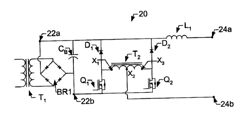
Figure 2 illustrates one embodiment of the buck regulator circuit 20 of the
present invention. The buck regulator circuit includes positive and negative
input
terminals, 22a and 22b, respectively, connected to a rectifier bridge BRl,
which, in
turn, is connected to a line frequency transformer Tl. The transformer is
connected
to an AC voltage source, such as a wall outlet. The buck regulator circuit 20
further includes positive and negative load terminals, 24a and 24b,
respectively,
connected to a load, not shown. The load can be any machinery, control system,
etc. requiring regulated DC power. Connected between the positive input and
positive load terminals is an inductive element Ll.
Importantly, the buck regulator circuit of the present invention includes a
center-tapped auto-transformer T2. The center-tapped auto-transformer TZ has
an
intermediate tap XZ and first and second end taps, Xl and X3, respectively.
The
-5-
. 1. ~ ki '~ ~ i ~;
CA 02390243 2002-07-11
intermediate tap of the auto-transformer is connected to the negative load
terminal
24b. Connected to the first Xl and second X3 end taps of the center-tapped
auto-
transformer are first and second switches, Ql and QZ, respectively, and first
and
second diodes, Dl and D2, respectively. The first switch Ql is connected
between
the first end tap Xl of the center-tapped auto-transformer TZ and the negative
input
terminal 22b, and the first diode Dl is connected between the first end tap XI
and
the positive input terminal 22a. Similarly, the second switch Ql is connected
between the second end tap X3 of the center-tapped auto-transformer T= and the
negative input terminal 22b, and the second diode D2 is connected between the
second end tap X3 and the positive input terminal 22a. In some embodiments,
the
buck regulator circuit of the present invention may further include a
capacitive
element Cl connected between the positive and negative input terminals to
smooth
AC ripple in the circuit.
As mentioned above, the buck regulator circuit of the present invention is
capable of operating in two modes, where each mode of operation outputs two
different voltage levels. Further, in either mode, the buck regulator circuit
reduces
the current across the switches used in the circuit. The operation of the buck
regulator circuit of the present invention is discussed in greater detail
below.
In a first mode, the switches of the buck regulator circuit are operated in
parallel. In this mode, the switches, Ql and Qi, are switched to the same
state at
substantially the same time, such that both switches are in an "on" state at
the same
time and in an "off ' state at the same time. With reference to Figure 3A, in
the
parallel mode, when the switches, Ql and QZ, are in the "on" state, current
flows
from the capacitor Cl through the inductive element Ll and the load. From the
negative terminal of the load, the current flows through the center tap XZ of
the
auto-transformer to the first and second ends, Xl and X3. Finally, the current
flows
through the switches, Q~ and QZ, to the capacitor Cl. With reference to Figure
3B,
when the switches, Ql and Q2, are in the "ofd' state, the energy stored in the
inductive element Ll free wheels through load and the first and second diodes,
Dl
and D2.
Importantly, in this configuration, because current is flowing in both
directions in the auto-transformer TZ (i.e., from XZ to Xl and X2 to X3),
there is no
-6-
I. '! ll ': ~ ', ii
CA 02390243 2002-07-11
net flux in the auto-transformer T2. As such, no transformer action occurs,
and the
maximum voltage is provided to the load. In this arrangement, the regulator
circuit
of the present invention operates much like a conventional buck regulator.
Importantly, however, because the switches are configured in parallel, the
total
peak current in the circuit is divided between the two switches, as opposed to
flowing through only one switch. For example, if current across the load is
200
amps, then the current across each switch is approximately 100 amps per
switch.
As such, switches having lower current ratings and typically cheaper in cost
can be
used in the buck regulator circuit of the present invention.
In addition to operating in the parallel mode to provide a first voltage, the
switches of the buck regulator circuit of the present invention can also be
operated
in a push-pull mode to provide a second lower voltage. In the push-pull mode,
the
"on" time of the switches is alternated, such that only one switch is in the
"on"
state at a given time. As only one switch is "on" at a given time, current
flows
through the auto-transmitter Ti and causes a net flux. The auto-transformer
effectively turns down the load voltage through the circuit decreasing the
load
voltage to a second level and decreasing the current through each switch.
Specifically, with reference to Figure 3C, during the first cycle of the push-
pull mode, the first switch Ql is in the "on" state. In this instance, current
flows
from the capacitor CI, through the inductor Ll and load to the auto-
transformer TZ.
In the auto-transformer, the current flows from the center tap XZ to the end
tap Xl
and from there through the first switch Ql back to the capacitor Cl. By auto-
transformer action, the second end tap X3 of the auto-transformer becomes
positive
relative to the intermediate tap Xl. This positive difference causes current
to also
flow from the second end tap X3 through the second diode D2, inductor Ll,
load,
and back through the intermediate XZ and second end X3 taps of the auto-
transformer T2. With reference to Figure 3B, when the first switch is
transitioned
to the "off ' state and prior to the second switch being transitioned to the
"on" state,
the energy stored in the inductor Ll free wheels through the load to the
intermediate tap X2 of the auto-transformer T2. From the intermediate tap, the
current flows through to both the first and second end taps, Xl and X3, the
first and
second diodes, Dl and D2, and back to the inductive element Ll.
CA 02390243 2002-07-11
With reference to Figure 3D, after the first switch Q1 has been transitioned
to an "off ' state, the second switch Q2 is then transitioned to an "on"
state. Similar
to the operation when the first switch QI is "on," load current flows from the
capacitance element Cl, through the inductive element Ll, and the load. From
the
negative terminal 24B, the current flows to the intermediate tap Xz of the
auto-
transformer T2, to the second end tap X3, and then the second switch X2 to the
capacitor C~.
As current flows in the auto-transformer from the intermediate tap X2 to the
second end tap X3, a positive voltage is realized between the first end tap Xl
and
the intermediate tap X2. The positive voltage causes current to flow from the
first
end tap Xl through the first diode Dl, inductive element Ll, the load and
through
intermediate tap XZ and first end tap Xl of the auto-transformer T2.
With reference to Figure 3B, when the second switch QZ is again
transitioned to the "off' state and prior to the transition of the first
switch to the
1 S "on" position, the energy in the inductive element Ll again freewheels.
Specifically, the current flows from the inductive element Ll through the
load,
through the intermediate tap X2 to the first Xl and second X3 taps, the first
and
second diodes, DI and D2, to the inductive element L~.
As can be seen in Figures 3A-3D, when the first and second switches, Ql
and Q2, are operated in the push-pull mode, there is a net flux flow in the
auto-
transformer. This causes auto-transformer action, which steps down the voltage
across the load providing a second voltage. Further, the auto-transformer also
steps down the current through each of the switches when they are in the "on"
state. As such, not only does the buck regulator in the push-pull mode provide
a
second lower voltage output across the load, it also reduces the current
across the
switches.
In a typical embodiment, the auto-transformer T2 approximately halves the
voltage in the push-pull mode to the voltage output and the parallel mode. As
such, in one embodiment, the buck regulator of the present invention operates
as a
1:1 power source in the parallel mode and a 2:1 step-down power source in the
push-pull mode. Further, in both modes the current for each switch is
typically
halved reducing the required power rating for the switches.
_g_
~;~i.. s !.
CA 02390243 2002-07-11
The power loss in the switching elements is an important aspect of the buck
regulator circuit of the present invention. When operated in the parallel mode
the
circuit is functionally the same as a buck regulator with a single large
switch,
however several advantages still exist. First, a single switch large enough to
handle the load current may cost several times that of a smaller switch.
Second, as
the switches become larger, switching losses limit the maximum frequency at
which they can operate.
One possible solution would be to simply parallel two of the smaller
switches. This can be done, however, it requires that the switches be matched
for
both conduction and switching characteristics which may significantly increase
cost. If the switches are operated in parallel and not matched for their
conduction
and switching characteristics, one switch may carry much more current than the
other resulting in failure. At the switching frequencies common in this type
of
regulator, switching losses, and more specifically "turn ofd' losses can
easily
become the predominant losses in the system. If not matched for switching
characteristics, the slower switch can carry all of the "turn off ' losses
resulting in
failure. In the case of the present invention, if one switch turns "on" or
"off," prior
to the other, the unbalanced current in the auto-transformer causes a net flux
to
exist in the transformer. This net flux causes transformer action, which in
turn,
limits the current in the conducting switch to one half of the load current.
As a
result of the auto-transformer, no switch can be required to conduct more than
one
half of the load current.
Although the switches in the push-pull mode have the same "on" time as
the one switch QB of the conventional buck regulator, the push-pull mode does
provide advantages in terms of the inductive element Ll. Specifically, output
voltage ripple is directly related to the operation of the switch. The
frequency of
this ripple will determine the voltage loading on the inductive element Ll.
For
example, in the prior art buck regulator circuit 10 illustrated in Figure 1,
if the
switch transitions between "on" and "off' states at 25 kHz, the ripple output
will
have a frequency of 25 kHz and it will load the inductive element Ll at a
first rate.
However, in the case of push-pull switches, the switches are operated
180° out of
phase. If both switches are operating at 25 kHz, then essentially together
they
-9-
i~i~~ i; i~
CA 02390243 2002-07-11
operate at 50 kHz, which creates a 50 kHz ripple. The 50 kHz ripple loads the
inductive element Ll at a rate that is twice that of the first rate. This
effectively
allows a smaller, less expensive inductive element Ll to be used in the buck
regulator circuit.
S Alternatively, if the ripple frequency of the output is to be maintained at
25
kHz, the switching frequency of each switch can be reduced to 12.5 kHz. Since
the predominant losses can be switching losses, which are proportional to
switching frequency, it is possible to handle significantly higher load
current in the
alternating mode.
As mentioned, an important advantage of the present invention is the ability
to provide two voltage output levels while also reducing the current across
the
switches used the regulator circuit. The advantages of the buck regulator
circuit of
the present invention may be beneficial for many different applications. As an
example, one embodiment of the buck regulator circuit of the present invention
can
be advantageously used in a welding or cutting system. In a welding or cutting
system, typically a first output voltage is required to initiate the welding
or cutting
process, but this high voltage level is not required to maintain the cutting
or
welding process, once initiated. While conventional buck regulators only
provide
one voltage, (i.e., the high level voltage required to initiate cutting or
welding), the
buck regulator circuit of the present invention can be used instead to provide
an
initial high voltage followed by a reduced voltage to sustain the welding or
cutting
process.
In this embodiment, the positive and negative output terminals, 22a and
22b, are connected to a rectifier bridge and power transformer that outputs 56
VAC. The positive and negative load terminals, 24a and 24b, are connected to a
welding or cutting system, (i.e., load). In this embodiment, when welding or
cutting is initiated, the buck regulator circuit of the present invention
operates the
switches in a parallel mode and outputs a load voltage of 75 VDC. After
welding
has been initiated, the switches of the buck regulator circuit of the present
invention are transitioned to operate in a push-pull mode. In the push-pull
mode,
due to the action of the auto-transformer, a voltage of approximately half
that of
the voltage output in the parallel mode, (i.e., approximately 37.5 VDC) is
output
-10-
f .. . i ; 1
CA 02390243 2002-07-11
across the load. As such, the buck regulator circuit of the present invention
provides at least two voltage levels allowing the welding or cutting system to
conserve energy in the welding process. Further, due to use of two switches
and
the auto-transformer, the current through each switch is half that of the load
current.
As discussed above, the first and second switches, Q~ and Q2, of the buck
regulator circuit of the present invention are controlled to operate in either
a
parallel mode or a push-pull mode. In typical embodiments, these switches are
logic field-effect transistors (FETs), such as J-FETs or MOSFETs, which can be
electronically controlled by a controller for precise operation. For example,
Figure
2 illustrates a control circuit 26 connected to the switches. The control
circuit
controls the "on" and "off ' states of the switches.
Although any general circuit may be used for the purpose of controlling the
switches, Figure 4 illustrates an embodiment of a control circuit designed and
implemented to test the buck regulator circuit of the present invention. The
control
circuit 26 includes positive and negative rails, 28a and 28b, for connection
to a
voltage source. Further, the control circuit includes a pulse width modulator
30
and two buffer drivers, 32a and 32b. The buffer drivers each include an
output, Si
and S2, respectively, for connection to the source of the switches, Ql and QZ,
and
an output, Gl and G2, for connection to the gate of the switches. The pulse
width
modulator includes a first circuit Pi for adjusting the width of the pulses
output by
the modulator and a second circuit PZ for adjusting the frequency of the
modulator.
Importantly, in one advantageous embodiment, the pulse width modulator
is a transistor logic ship TL594. This logic chip includes an enable pin that
25 when enabled outputs pulses to both buffer drivers at the same time to
drive the
switches in parallel, and when disabled, outputs pulses alternatively to the
buffer
drivers to drive the switches in a push-pull configuration. A selector switch
34 is
provided to alter the mode of the modulator. As such, the buck regulator
circuit of
the present invention can be operated to provide two separate voltage levels
based
30 on the position of the selector switch.
Many modifications and other embodiments of the invention will come to
mind to one skilled in the art to which this invention pertains having the
benefit of
-11-
CA 02390243 2002-07-11
the teachings presented in the foregoing descriptions and the associated
drawings.
Therefore, it is to be understood that the invention is not to be limited to
the
specific embodiments disclosed and that modifications and other embodiments
are
intended to be included within the scope of the appended claims. Although
specific
terms are employed herein, they are used in a generic and descriptive sense
only
and not for purposes of limitation.
-12-