Note: Descriptions are shown in the official language in which they were submitted.
CA 02390400 2002-07-03
BALLAST WITH PROTECTION CIRCUIT FOR
QUICKLY RESPONDING TO ELECTRICAL DISTURBANCES
00-1-250
Field of the Invention
The present invention relates to the general subject of circuits for
powering discharge lamps. More particularly, the present invention relates to
a
ballast that includes a circuit for detecting and responding to electrical
disturbances such as output arcing.
Background of the Invention
Ballasts for gas discharge lamps provide high ignition voltages for
starting the lamps. The ignition voltages supplied by preheat type ballasts
are
typically on the order of several hundred volts (e.g., 500 volts peak), while
those
provided by instant-start type ballasts may exceed 1000 volts peak. As a
consequence of these high output voltages, ballasts are subject to the problem
of
output arcing.
Output arcing may occur in any of a number of different ways. For
example, in fluorescent lighting installations, it is a common practice to
replace
failed lamps while AC power is applied to the ballast. This practice is
referred
to as "live" relamping. During live relamping, as a lamp is being removed or
inserted, a momentary arc may form between the fixture socket contacts and a
pin of the lamp. As another example, a sustained arc (as opposed to a
momentary arc) arc may occur due to poor connections in the output wiring or
the lamp sockets, or if a lamp is improperly installed such that a small gap
exists
between the lamp pins and the contacts within the fixture sockets.
Arcing is generally acknowledged to cause degradation of the contacts in
the fixture sockets and undue stress on components within the ballast.
Sustained arcing is especially undesirable. In order to minimize any ill
effects
due to arcing, it is important that the arc be promptly extinguished. Thus, a
need exists for a ballast having a protection circuit that quickly detects an
output
arc and then takes appropriate action to quickly extinguish the arc. A further
need exists for a protection circuit that is economical and easy to implement
CA 02390400 2002-07-03
2
within existing ballasts. Such a ballast and protection circuit would
represent a
considerable advance over the prior art.
Brief Description of the Drawings
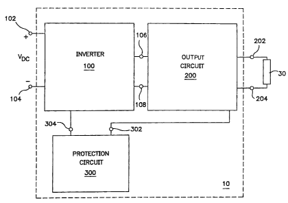
Fig. 1 is a block diagram schematic of a ballast with a protection circuit,
in accordance with first and second preferred embodiments of the present
invention.
Fig. 2 describes an example of an electrical disturbance to which the
disclosed protection circuit is responsive, in accordance with the preferred
embodiments of the present invention.
Fig. 3 is a schematic diagram of a ballast with a driven inverter and a
series resonant output circuit, wherein a disturbance is monitored in the
resonant
circuit, in accordance with the first preferred embodiment of the present
invention.
Fig. 4 is a schematic diagram of a ballast with a driven inverter and a
series resonant output circuit, wherein a disturbance is monitored at an
output
connection of the ballast, in accordance with the second preferred embodiment
of the present invention.
Fig. 5 is a block diagram schematic of a ballast with a protection circuit,
in accordance with a third preferred embodiment of the present invention.
Fig. 6 is a schematic diagram of a ballast with a self oscillating inverter,
in accordance with a third preferred embodiment of the present invention.
6 ~ ii.'~ il~ I GI
CA 02390400 2002-07-03
3
Detailed Description of the Preferred Embodiments
Fig. 1 describes a ballast 10 for powering a gas discharge lamp load 30.
Ballast 10 includes an inverter 100, an output circuit 200, and a protection
circuit 300. During operation, inverter 100 provides a high frequency (e.g.,
20
kilohertz or greater) voltage at an inverter output 106,108. Output circuit
200 is
coupled to inverter output 106,108, and includes output connections 202,204
for
connection to gas discharge lamp load 30. Protection circuit 300 is coupled to
inverter 100 and output circuit 200. During operation, protection circuit 300
monitors a signal within output circuit 200. In response to a disturbance
wherein at least a portion of the signal exhibits a time-rate-of change that
substantially exceeds the time-rate-of change of the signal during normal
operation of the ballast and gas discharge lamp load, protection circuit 300
disables inverter 100 for at least a predetermined period of time (e.g., 100
milliseconds).
Typical disturbances to which protection circuit 300 is responsive
include disconnection of a lamp from the ballast and occurrence of an arcing
condition at the ballast output connections 202,204. For example, as
illustrated
in FIG. 2, such disturbances generally cause at least one transient spike 44
having a relatively large time-rate-of change to appear in the monitored
signal
40. It should of course be appreciated that the waveform in FIG. 2 is a gross
simplification of what occurs in reality; most disturbances, such as output
arcing, will cause multiple transient spikes to appear in the monitored
signal.
When lamp load 30 is operating in a normal manner, the monitored signal will
be a periodic signal having a period. For example, as illustrated in FIG. 2,
the
monitored signal may be a substantially sinusoidal signal. During normal
operation of the ballast and lamp load, the maximum time-rate-of change of a
sinusoidal signal occurs at the zero crossings 42, and is substantially less
than
the maximum time-rate-of change of transient 44.
Advantageously, following a disturbance in the signal within output
circuit 200, protection circuit 300 is capable of disabling inverter 100
within a
response time that is less than twice the period of the high frequency voltage
at
~~ I I., '~, I~~I~i. ill ~ '
CA 02390400 2002-07-03
4
the inverter output. For typical ballast applications, where the frequency of
the
voltage at the inverter output is designed to be 20 kilohertz or greater, this
corresponds to a response time that is less than 100 microseconds.
Preferably, inverter 100 and protection circuit 300 are further operable
such that inverter 100 is re-enabled after the predetermined period of time
(e.g.,
100 milliseconds) elapses. This feature is desirable in order to prevent
permanent shutdown of the ballast (i.e., necessitating that power to the
ballast be
cycled off and on in order to reset the ballast) in the event of false
detection due
to a momentary power line transient or any of a number of anomalous
phenomena that pose no sustained threat to ballast reliability or safety.
Turning now to FIG. 3, in a first preferred embodiment of the present
invention, inverter 100 comprises first and second input terminals 102,104,
first
and second output terminals 106,108, a pair of inverter switches 110,120, an
inverter drive circuit 130, and a DC supply circuit that includes resistor
134,
1 S capacitor 136, capacitor 140, zener diode 142, and diode 144. Second
output
terminal 108 is coupled to a circuit ground node 60.
During operation, inverter 100 receives a substantially direct current
(DC) voltage, V~, at inverter input terminals 102,104 and provides a high
frequency squarewave voltage between output terminals 106,108. V~ can be
provided by any of a number of known arrangements that accept an ordinary AC
power-line voltage (e.g., 120 VAC, 277 VAC) and provide a filtered DC output
voltage. For example, VDT can be provided by a full-wave rectifier followed by
a boost converter.
Drive circuit 130 is coupled to inverter switches 110,120, and has a
supply input 132 for receiving a DC supply voltage. During operation, as long
as the DC supply voltage is greater than a predetermined value, drive circuit
130
turns inverter switches 110,120 on and off in a substantially complementary
manner and at a high frequency rate that is preferably in excess of 20
kilohertz.
If the DC supply voltage falls below a predetermined value, drive circuit 130
ceases switching of inverter switches 110,120. Drive circuit 130 may be
implemented using a custom integrated circuit (IC) or any of a number of
CA 02390400 2002-07-03
S
commercially available integrated circuits, such as the IR2155 "high-side
driver" integrated circuit manufactured by International Rectifier.
Resistor 134 functions as a startup resistor that, following application of
power to ballast 10, supplies current for initially charging capacitor 136 to
a
voltage sufficient to activate driver circuit 130 and initiate inverter
switching.
Once inverter 100 begins to operate, capacitor 140 and diode 144 function as a
bootstrap supply that uses energy in output circuit 200 to maintain the
voltage
across capacitor 136 at a level sufficient to keep driver circuit 130 on.
Zener
diode 142 serves as a protective device that prevents the voltage at supply
input
132 from rising, under certain circumstances, to levels that might be harmful
to
drive circuit 130.
Protection circuit 300 has an input 302 and an output 304. Input 302 is
coupled to output circuit 200. Output 304 is coupled to inverter 100. During
operation, protection circuit 300 monitors a signal within output circuit 200
and,
1 S in response to occurrence of a disturbance in the signal, disables
inverter 100 for
a limited period of time. A disturbance is deemed to have occurred when at
least a portion of the signal has a time-rate-of change that substantially
exceeds
the time-rate-of change of the signal during normal operation of the ballast
and
lamp load.
Referring again to FIG. 3, in a first preferred embodiment of the present
invention, output circuit 200 comprises first and second output connections
202,204, a resonant inductor 210, a resonant capacitor 220, a direct current
(DC)
blocking capacitor 230, and a current-sensing resistor 240. Output connections
202,204 are adapted for connection to a lamp load 30 comprising at least one
gas discharge lamp 32. Resonant inductor 210 is coupled between first output
terminal 102 and first output connection 202. Resonant capacitor 220 is
coupled between first output connection 220 and circuit ground node 60. DC
blocking capacitor 230 is coupled between second output connection 204 and
circuit ground node 60. Current-sensing resistor 240 interposed between
resonant capacitor 220 and circuit ground node 60. Input 302 of protection
circuit 300 is coupled to current-sensing resistor 240. In this configuration,
the
CA 02390400 2002-07-03
6
signal monitored by protection circuit 300 is the current that flows through
resonant capacitor 220.
Output 304 of protection circuit 300 is coupled to the supply input 132
of drive circuit 130. During operation, and in response to a disturbance,
protection circuit 300 turns off drive circuit 130 by coupling supply input
132 to
circuit ground 60 for a predetermined period of time. Once supply input 132 is
coupled to ground, the voltage at supply input 132 will quickly fall below the
predetermined value necessary to keep drive circuit 130 active, so drive
circuit
130 will turn off and inverter switching will cease. As long as supply input
132
is coupled to ground, the supply voltage will be prevented from reaching a
value
necessary to reactivate drive circuit 130.
Upon expiration of the predetermined period of time (e.g., 100
milliseconds), protection circuit 300 will cease coupling supply input 132 to
ground, at which point capacitor 136 will begin to charge up via startup
resistor
134. Once the voltage across capacitor 136 reaches a predetermined startup
threshold (the exact value of which is determined by the actual device used to
implement drive circuit 130), drive circuit 130 will turn on and begin to
switch
the inverter switches on and off. With the inverter now operating again,
energy
sufficient to maintain the supply voltage above the turn-off threshold is
supplied
by the bootstrapping circuit consisting essentially of capacitor 140 and diode
144. In this way, protection circuit 300 allows inverter 100 to automatically
restart.
A preferred circuit implementation of protection circuit 300 is now
explained with reference to FIG. 3 as follows. Protection circuit 300 includes
a
latching device 310 and a triggering circuit 330. Latching device 310 is
coupled
between output 304 and circuit ground 60, and has a control terminal 312
coupled to a first node 334. During operation, latching device 310 is
functional
to: (1) turn on and couple output 304 to circuit ground in response to the
voltage
at control terminal 312 reaching a predetermined triggering voltage (e.g., 1
volt); and (2) remain on for as long as the amount of current flowing through
the
device (i.e., from protection circuit output 304 to circuit ground 60) exceeds
a
predetermined holding current (e.g., 10 milliamperes); the predetermined
~,,;,i 1~1 ~I
CA 02390400 2002-07-03
7
holding current is dictated by the electrical characteristics of the
components)
used to implement latching device 310. Triggering circuit 330 is coupled to
input 302, first node 334, and circuit ground 60. During operation, triggering
circuit 330 is functional, in response to a disturbance, to provide sufficient
voltage (e.g., 1 volt) to turn on latching device 310.
Preferably, latching device 310 is implemented using a silicon controlled
rectifier (SCR) 320. SCR 320 has an anode 322 coupled to protection circuit
output 304, a cathode 324 coupled to circuit ground 60, and a gate terminal
326
coupled to first node 334.
As described in FIG. 3, triggering circuit 330 preferably includes a
capacitor 332 and a resistor 336. Capacitor 332 is coupled between protection
circuit input 302 and first node 334. Resistor 336 is coupled between first
node
334 and circuit ground 60. The capacitance of capacitor 332 and the resistance
of resistor 336 are chosen such that a disturbance with a specified time-rate-
of
change in voltage will produce sufficient voltage across resistor 336 to turn
on
SCR 320. The resistance of resistor 336 and the capacitance of capacitor 332
(i.e., the "RC" time constant) governs the speed at which sufficient voltage
will
be developed to turn on SCR 320 in response to a specified disturbance. In
this
regard, for a given value of resistance for resistor 336, a smaller
capacitance will
result in SCR 320 turning on in response to disturbances with a faster rate-of
rise, while a smaller capacitance will result in SCR 320 turning on in
response
to disturbances with a slower rate-of rise. Thus, one can adjust the
sensitivity of
the trigger circuit to respond to those disturbances having a time-rate-of
change
that exceeds a specified quantity. However, too small a capacitance will
deprive
resistor 336 of the current needed to develop sufficient voltage to activate
SCR
320 following occurrence of a disturbance, and too large a capacitance will
result in SCR 320 being turned on preemptively (i.e., even though a specified
disturbance has not occurred). In a prototype ballast, capacitor 332 was set
at
220 picofarads, resistor 336 was set at 330 ohms, and current-sensing resistor
240 was set at 3.3 ohms.
Preferably, protection circuit 300 further comprises a resistor 340
coupled between protection circuit output 304 and anode 322 of SCR 320.
CA 02390400 2002-07-03
Resistor 340 functions as a current-limiting resistor for limiting the
potentially
high peak current that would otherwise flow through SCR 320 following turn
on. The potentially high peak current is attributable to the fact that
capacitor
136 acts as a low impedance source capable of supplying large amounts of
current for a very limited period of time. In a prototype ballast, resistor
340 was
set at 10 ohms.
The detailed operation of ballast 10 and protection circuit 300 is now
explained with reference to FIG. 3 as follows.
When power is initially applied to ballast 10, drive circuit 130 is off.
Capacitor 136 begins to charge up via resistor 134. Once the voltage across
capacitor 136 reaches a minimum value (e.g., 9 volts) necessary to activate
drive
circuit 130, drive circuit 130 turns on and begins to commutate inverter
transistors 110,120. With inverter switching now taking place, output circuit
200 becomes energized and soon develops sufficient voltage to ignite the
1 S lamps) in lamp load 30. Energy from output circuit 200 is used to
bootstrap the
inverter via capacitor 140 and diode 144, and the voltage across capacitor 136
and at DC supply input 132 quickly reaches its steady-state operating value
(e.g., 15 volts).
With ballast 10 and lamp load 30 operating in a normal manner, the
voltage across current-sensing resistor 240 is a substantially sinusoidal
waveform having a frequency identical to the operating frequency of inverter
100. During this time, the current through capacitor 332 and the voltage
across
resistor 336 will be very low (e.g., approximately zero). Consequently, SCR
320 will remain off, and the voltage across capacitor 136 and at DC supply
input
132 will remain at its normal steady-state operating value of approximately 15
volts.
If an output arc or other type of disturbance occurs, the voltage across
current-sensing resistor 240 will include one or more transient spikes having
a
large time-rate-of change (i.e., a large dV/dt). The large time-rate-of change
of
the transient spikes) will rapidly cause a substantial current to flow through
capacitor 332 and resistor 336. Consequently, the voltage across resistor 336
will become large enough (e.g., 1 volt or greater) to turn on SCR 320. Once
CA 02390400 2002-07-03
9
activated, SCR 320 couples DC supply input 132 to circuit ground 60 via
resistor 340, causing the voltage across capacitor 136 to fall rapidly. Once
the
voltage across capacitor 136 falls below a level (e.g., 8 volts) necessary to
maintain operation of drive circuit 130, drive circuit 130 will turn off and
inverter switching will cease, thus terminating the disturbance. In this way,
protection circuit 300 rapidly detects a disturbance and quickly disables
inverter
100 so as to prevent any damage or undue stress to the ballast.
Once activated, and even after inverter 100 has been deactivated, SCR
320 will remain on and continue to discharge capacitor 136 as long as the
voltage across capacitor 136 remains high enough to supply at least the
minimum holding current (e.g., 10 milliamperes) required to maintain
conduction through SCR 320. As the voltage across capacitor 136 approaches
zero, the current through SCR 320 falls below the minimum holding current and
SCR turns off. At this point, the inverter startup sequence described above
will
be repeated and the inverter will once again begin to operate. In this way,
following a disturbance, protection circuit 300 quickly turns inverter 100 off
for
a limited period of time sufficient to extinguish the disturbance and protect
the
ballast, but then allows inverter 100 to automatically restart.
FIG. 4 describes a second preferred embodiment of the present
invention, wherein the output circuit is modified to provide a ballast 10'
that
supplies filament heating to a lamp 32 having a first filament 34 and a second
filament 36. Output circuit 200' includes all of the components previously
recited with regard to output circuit 200 in FIG. 3, except for current-
sensing
resistor 240, and further comprises a third output connection 206, a fourth
output connection 208, a first auxiliary winding 212, and a second auxiliary
winding 214. First auxiliary winding 212 and second auxiliary winding 214 are
magnetically coupled to resonant inductor 210. First filament 34 and first
auxiliary winding 212 are coupled to first output connection 202 and third
output connection 206. Second filament 36 and second auxiliary winding 214
are coupled to second output connection 204 and fourth output connection 208.
p, 'il I I I II
CA 02390400 2002-07-03
As described in FIG. 4, protection circuit input 302 is coupled to the
fourth output connection (compare with the arrangement of FIG. 3, where
protection circuit input 302 is coupled to current-sensing resistor 240 in
series
with resonant capacitor 220). In response to a disturbance, such as an arcing
5 condition, the voltage existing between fourth output connection 208 and
circuit
ground 60 will include one or more transient spikes having a time-rate-of
change that substantially exceeds the time-rate-of change during normal
operation of the ballast and lamp.
The preferred structure and detailed operation of protection circuit 300
10 in the embodiment described in FIG. 4 is substantially the same as that
which
was previously discussed with regard to the embodiment described in FIG. 3.
Whereas the embodiments previously described with reference to FIGS.
3 and 4 are suitable for ballasts with driven inverters, FIGs. 5 and 6
describe a
third preferred embodiment of the present invention that is suitable for
ballasts
that include a self oscillating inverter.
Referring to FIG. 5, ballast 20 comprises an inverter 400, an output
circuit 500, a protection circuit 600, and a current-feed inductor 700.
Inverter
400 has input terminals 402,404 and output terminals 406,408. During
operation, inverter 400 receives a substantially direct current (DC) voltage,
VDC, at input terminals 402,404, and provides a high frequency (e.g., 20
kilohertz or greater) voltage between inverter output terminals 406,408.
Output
circuit 500 is coupled to inverter output terminals 406,408, and includes
output
connections 502,504 for connection to gas discharge lamp load 30.
Turning to FIG. 6, output circuit 500 includes a resonant capacitor 550
and an output transforner 510. Resonant capacitor 550 is coupled between
inverter output terminals 406,408. Output transformer 510 includes a primary
winding 520, a secondary winding 530, and an auxiliary winding 540. Primary
winding 520 is coupled between inverter output terminals 406,408. Secondary
winding 530 is coupled to output connections 502,504. Auxiliary winding 540
is coupled to inverter 400, and includes a first end 542 and a second end 544.
As will be discussed further below, auxiliary winding 540 provides base drive
CA 02390400 2002-07-03
11
for operating inverter 400. Output circuit 500 further includes a ballasting
capacitor 560 that limits the operating current provided to lamp load 30.
Protection circuit 600 is coupled to inverter 400 and auxiliary winding
540 of output transformer 510. During operation, protection circuit 600
monitors a voltage signal (e.g., the voltage across auxiliary winding 540)
associated with output transformer 510. In response to occurrence of a
disturbance in the voltage signal, protection circuit 600 disables inverter
400 for
a predetermined period of time. A disturbance is deemed to have occurred when
at least a portion of the voltage signal has a time-rate-of change (i.e.,
dV/dt) that
substantially exceeds the time-rate-of change of the signal during normal
operation of the ballast and lamp load 30.
Advantageously, following a disturbance in the voltage signal, protection
circuit 600 is capable of disabling inverter 400 within a response time that
is
less than twice the period of the high frequency voltage between inverter
output
terminals 406,408. For typical ballast applications, where the frequency of
the
voltage at the inverter output is designed to be 20 kilohertz or greater, this
corresponds to a response time that is less than 100 microseconds.
Preferably, inverter 400 and protection circuit 600 are further operable
such that inverter 400 is re-enabled after the predetermined period of time
(e.g.,
100 milliseconds) elapses. This feature is desirable in order to prevent
permanent shutdown of the ballast (i.e., necessitating that power to the
ballast be
cycled off and on in order to reset the ballast) in the event of false
detection due
to a momentary power line transient or any of a number of anomalous
phenomena that pose no sustained threat to ballast reliability or safety.
As described in FIG. 6, protection circuit 600 includes a first input 604
coupled to the first end 542 of auxiliary winding 540, and a second input 602
coupled to the second end 544 of auxiliary winding 540. Inverter 400 includes
a
pair of inverter switches 410,420 connected in a push-pull configuration. Each
inverter switch 410,420 has a control input 412,422 for receiving a control
voltage that turns the switch on and off. Auxiliary winding 540 is coupled to
inverter switches 410,420 and provides the control voltage. Resistor 430,
resistor 440, diode 414, and diode 424 operate in conjunction with auxiliary
CA 02390400 2002-07-03
12
winding 540 to effect switching of inverter switches 410,420. During normal
operation of the ballast and lamp load, auxiliary winding 540 has a
substantially
sinusoidal voltage that turns the inverter switches on and off in a
substantially
complementary manner. In response to a disturbance, protection circuit 600
disables inverter 400 by forcing the control voltage of at least one of the
inverter
switches to a negative value, and then keeping the control voltage negative,
for a
predetermined period of time.
Preferably, protection circuit 600 comprises a pull-down circuit 640 and
a negative voltage source 610. Pull-down circuit 640 is coupled to first input
604, second input 602, and negative voltage source 610. In response to a
disturbance, pull-down circuit 640 couples first input 604 to negative voltage
source 620 for a limited period of time. Negative voltage source 610 is
coupled
between second input 602 and circuit ground 60
Pull-down circuit 640 includes a latching device 650 and a triggering
circuit 670. Latching device 650, which is preferably realized as a silicon-
controlled rectifier (SCR) 660, is coupled between first input 604 and
negative
voltage source 610, and includes an anode 662, a cathode 664, and a gate 666.
During operation, in response to a voltage between gate 666 and cathode 664
reaching a predetermined triggering voltage, SCR 660 turns on and couples
anode 662 to cathode 664. Once turned on, SCR 660 remains on for as long as
the amount of current flowing from anode 62 to cathode 664 exceeds a
predetermined holding current (e.g., 10 milliamperes). Triggering circuit 670
is
coupled to second input 602, gate 666, and cathode 664. In response to a
disturbance in the voltage across auxiliary winding 540, triggering circuit
670
provides sufficient voltage between gate 666 and cathode 664 to quickly turn
on
SCR 660. Triggering circuit 670 includes a capacitor 672 and a resistor 676.
Capacitor 672 is coupled between second input 602 and a first node 674.
Resistor 676 is coupled between first node 674 and cathode 664 of SCR 660. In
a prototype ballast, capacitor 672 was set at 100 picofarads and resistor 676
was
set at 1 kilahm.
Triggering circuit 670 optionally includes a diode 678 placed in parallel
with resistor 676. Diode 678 prevents large negative gate-to-cathode voltages
~~. L_ p.,. ~ ~ ~~ I ~I
CA 02390400 2002-07-03
13
from being applied to SCR 660, and thus protects SCR 660 from potential
damage.
Pull-down circuit 640 optionally includes a diode 642 coupled between
first input 604 and anode 662 of SCR 660. It is believed that diode 642 serves
to prevent self triggering of SCR 660 under normal high-frequency conditions
that occur in ballast 20.
As described in FIG. 6, negative voltage source 610 includes a first
diode 612, a first resistor 620, a capacitor 624, a second resistor 626, and a
second diode 628. First diode 612 has a cathode 614 coupled to second input
602 and an anode 616 coupled to a second node 618. First resistor 620 is
coupled between second node 618 and a third node 622. Capacitor 624 and
second resistor 626 are each coupled between third node 622 and circuit ground
60. Second diode 628 has an anode 630 coupled to third node 6223 and a
cathode 632 coupled to circuit ground 60.
The detailed operation of ballast 20 and protection circuit 600 is now
explained with reference to FIG. 6 as follows.
When power is initially applied to ballast 20, a small amount of energy is
provided to the base of transistor 410 via resistor 440, and causes transistor
410
to turn on. This energizes output circuit 500 and an alternating voltage
develops
across auxiliary winding 540. As the voltage across auxiliary winding 540
alternates, transistors 410 and 420 are turned on and off in a substantially
complementary manner. Output circuit 500 soon develops sufficient voltage to
ignite the lamps) in lamp load 30.
With ballast 20 and lamp load 30 operating in a normal manner, the
voltage across auxiliary winding 540 is a substantially sinusoidal waveform
having a frequency identical to the operating frequency of inverter 400 and
varying between about +12 volts and -12 volts. During this time, pull-down
circuit 640 is inactive and remains so until such time as a disturbance is
detected
in the voltage across auxiliary winding 540. Negative voltage source 610 uses
the negative half cycles of the voltage across auxiliary winding 540 to
develop a
voltage of approximately -3 volts across capacitor 624. The resistances of
resistor 620 and resistor 626 determine the value of the negative voltage
across
~~ . 'il I J. I fl
CA 02390400 2002-07-03
14
capacitor 624. In a prototype ballast, resistors 620,626 were each set at 470
ohms.
If an output arc or other type of disturbance occurs, the voltage across
auxiliary winding 540 will include one or more transient spikes having a large
time-rate-of change. The large time-rate-of change of the transient spikes)
will
rapidly cause a substantial current to flow through capacitor 672 and resistor
676. Consequently, the voltage across resistor 676 will become large enough
(e.g., 1 volt or greater) to turn on SCR 660. Once activated, SCR 660 couples
the base 412 of transistor 410 to a negative voltage (e.g., -2 volts at the
moment
that SCR 660 is first turned on), and thus terminates oscillation in inverter
400
for at least a limited period of time. In this way, protection circuit 600
rapidly
detects a disturbance and quickly disables inverter 400 so as to prevent any
damage or undue stress to the ballast.
Once activated, and even after inverter 400 has been disabled, SCR 660
will remain on (due to holding current supplied via resistor 430 and diode
414)
and prevent the inverter from restarting as long as the voltage across
capacitor
624 remains sufficiently negative to maintain a current through SCR 660 that
is
greater than the minimum holding current of the device (e.g., 10
milliamperes).
As the voltage across capacitor 624 becomes less and less negative, the
current
flowing through SCR 660 decreases. Once the current flowing through SCR
660 falls below the minimum holding current, SCR 660 turns off (because it is
desirable to ensure that the inverter remains off for at least 100
milliseconds or
so following occurrence of a fault, and the capacitance of capacitor 624 at
least
partially governs how long SCR 660 will remain on, it is recommended that
capacitor 624 be set at a large value such as 1000 microfarads). At this
point,
the inverter startup sequence described above will be repeated and the
inverter
will once again begin to operate. In this way, following a disturbance,
protection circuit 600 quickly turns inverter 400 off for a limited period of
time
sufficient to extinguish the disturbance and protect the ballast, but then
allows
inverter 400 to automatically restart.
Although the present invention has been described with reference to
certain preferred embodiments, numerous modifications and variations can be
CA 02390400 2002-07-03
15
made by those skilled in the art without departing from the novel spirit and
scope of this invention.
What is claimed is: