Note: Descriptions are shown in the official language in which they were submitted.
I ~ d~I II CA 02390750 2002-06-14
~ r
CFM 02629
TITLE OF THE INVENTION
INK-JET PRINTHEAD BOARD, INK-JET PRINTHEAD, AND
INK-JET PRINTING APPARATUS
FIELD OF THE INVENTION
The present invention relates to a printhead
board, a printhead using the board, and a printing
apparatus on which the printhead is mounted.
BACKGROUND OF THE INVENTION
Ink-jet printing is a printing method with a more
prominent feature than other printing methods because
of little printing noise and high-speed printing.
In the printhead of a conventional printing
apparatus which adopts this printing method, orifices
formed to discharge a liquid such as ink, and
electrothermal transducers (heaters) which communicate
with the orifices and generate, as energy generation
elements for discharging ink, predetermined heat energy
in order to heat and discharge droplets of ink or the
like are arranged on a printhead element board (to be
also referred to as a heater board "HB").
Further, a plurality of drivers for driving the
respective heaters, a memory which temporarily stores
printing data input from a printing apparatus in order
to transfer serial printing data as parallel data to
- 1 -
CA 02390750 2002-06-14
the respective drivers, and a logic circuit such as a
latch circuit which holds data output from the memory
in order to output the data at a predetermined timing
are conventionally mounted on the same board (HB) in
addition to a plurality of heaters.
The printhead board requires (1) a power supply
for driving the heaters and (2) two power supplies for
driving the memory, logic circuit, and the like. The
power supply for the logic circuit generally uses a
power supply voltage of 5 V. This power supply is
unified to an IC power supply for a CPU, memory, and
the like on the printing apparatus main body. This can
eliminate the needs for preparing a dedicated logic
power supply, and can achieve space reduction of the
circuit layout, downsizing, and cost reduction.
In general, a parallel interface is employed as
an interface for connecting an ink-jet printer and,
e.g., a personal computer which controls the printer.
In this case, the logic power supply voltage (VL) of
the printer main body is 5 V, and the ink-jet printhead
board in the head also uses 5 V for the logic power
supply. The above-described prior art, therefore, sets
VL to 5 V. The logic voltage VL of 5 V has been used
because some ICs require a power supply of 5 V in the
ICs of the internal printer circuit.
In recent years, it becomes disadvantageous to
prepare 5 V for the logic power supply of the printer
- 2 -
~ 11 i .1 1 kI
CA 02390750 2002-06-14
i 1
main body in terms of the cost and size along with
improvements in IC technique and the use of a new
interface. The recent mainstream of the logic power
supply voltage VL of the printer main body is shifting
to 3.3 V.
However, it is difficult to simply optimize the
logic power supply voltage to 3.3 V because the head
board mixedly bears a logic circuit and a
high-breakdown-voltage driver for driving a heater.
Several problems posed upon decreasing the logic
power supply voltage of a conventional head board from
5 V to 3.3 V will be explained.
(1) Problem on Operation Speed
A decrease in the image data transfer ability
(operation speed) of an ink-jet printhead board will be
described as one of the problems.
Fig. 15 shows an arrangement in the ink-jet
printhead board. In Fig. 15, reference numeral 1003
denotes each pad for receiving an external signal. The
pads 1003 have a VDD terminal 1006 for receiving a
logic power supply voltage, a VH terminal 1008 for
receiving a heater driving power supply voltage, a GNDH
terminal 1005 connected to ground, a CSS terminal 1007,
and the like. Logic circuits 1002 such as a shift
register for receiving serial image data and outputting
parallel data, drivers 1001 for driving heaters,
heaters 1004, and the like are arranged on a single
- 3 -
CA 02390750 2002-06-14
silicon board.
Fig. 16 shows in detail a case in which 640-bit
heaters are formed. In this case, 40 bits out of the
640-bit heaters are simultaneously driven at maximum.
This operation is repeated 16 times to drive all the
640-bit heaters (one cycle). Fig. 17 shows the
timings. A speed required to send image data when all
the 640 bits are driven at a driving frequency of 15
kHz (used in existing products) necessary for
predetermined high-speed printing will be explained.
The frequency of 15 kHz has a cycle of 66.67 S.
Image data of 40 bits must be transferred by 16 time
divisions (blocks) within this period. The image data
transfer rate is calculated as at least 12 MHz or
higher. This rate is not so high for a general CPU or
the like. For an ink-jet printhead, however, 12 MHz is
not low because a carriage to be driven and a main body
are connected by a long flexible board or the like and
the carriage must be downsized for a compact printer.
A decrease in transfer ability when the logic
power supply voltage is decreased from 5 V to 3.3 V in
this situation will be explained with reference to
Figs. 18A and 18B. Fig. 18A is a graph showing the
relationship between the voltage of a logic signal
(power supply) and the maximum CLK frequency capable of
transferring image data.
As shown in Fig. 18A, the CLK frequency tends to
- 4 -
CA 02390750 2002-06-14
Fr r
decrease as the voltage of the logic signal (power
supply) decreases. This is because the drivability of,
e.g., a CLK input circuit portion for transferring
image data and that of a MOS transistor used in a shift
register unit degrade at the same time as a decrease in
logic power supply voltage directly used as the gate
voltage of a CMOS. As shown in Fig. 18A, the
drivability (drain current Id) decreases with a
decrease in gate voltage.
The ink-jet printhead board must attain a
satisfactory temperature rise by driving heaters on the
board. This is a characteristic ability demanded of
the ink-jet printhead board for discharging ink by
heaters. Fig. 18B is a graph showing the relationship
between the board temperature and the maximum CLK
frequency. As shown in Fig. 18B, the ability is poor
at a logic power supply voltage of 3.3 V, and as the
temperature rises, tends to further degrade.
As described above, appropriate circuit operation
has been attained at a CLK frequency of 12 MHz for 5 V.
As the logic power supply voltage decreases to, e.g.,
3.3 V, the operation speed must be increased.
(2) Noise Problem
A voltage drop by the impedance of a power line
or a malfunction by the voltage drop generated by the
impedance of the power line or a noise component such
as overshooting may occur under the influence of
- 5 -
p, ~I: II Il 3 I II i
CA 02390750 2002-06-14
ri
increases in speed and the number of bits in a recent
printhead and a printing apparatus (printer) using the
printhead.
For example, for a typical A4-printer, the length
of a power cable for a flexible board or the like which
extends from the power supply of a main body to a head
is about 40 cm. The resistance (R) component of the
cable is about 20 mO to 100 mO though it changes
depending on the cable material and the number of
parallel-connected lines. The inductance (L) component
is about 0.1 H to 0.5 H. The parasitic impedance of
the power line is a contact resistance at the contact
with the head or the capacitance (C) component of the
head. The contact resistance is about 30 mSa to 200 mO
though it changes depending on the contact material and
the number of pads used as power supply terminals. The
capacitance is about 10 pF to 100 pF.
A current flowing through the power line is about
150 mA per segment, and is 0.9 A when the maximum
number of simultaneously driven segments per color is
16. In a recent 6-color printer, a total instantaneous
current is as large as 5.4 A.
If the 5.4-A current flows through the
above-mentioned power line having impedance components
R, L, and C, overshooting causes ringing, which
fluctuates the voltage of the power line. The voltage
fluctuation is about 0.5 V to 1.0 V in actual
- 6 -
CA 02390750 2002-06-14
measurement and electric circuit simulation.
In particular, the voltage fluctuation generated
in the GND line of a driver transistor can cause a
current driving malfunction. A means for preventing
any malfunction even upon voltage fluctuations must be
adopted.
(3) Problem on Common Voltage in Logic Unit
In a recent printhead and a printing apparatus
(printer) using the printhead, the logic signal voltage
tends to be decreased for a higher-speed heater driving
circuit and external signal processing circuit such as
a CPU and a finer design rule. The logic signal
voltage is abruptly shifting to the current voltage of
5 V to 3.3 V.
The voltage of the CPU is decreased as the
manufacturing process becomes finer. For example, the
power supply voltage is predicted to be about 2.0 V in
the use of a 0.5-,um rule process, and 1.5 V or lower
in the use of a 0.15 to 0.18- m rule process. It is
important for cost reduction of the overall apparatus
in terms of voltage sharing to set the signal voltage
of the external processing circuit and the internal
logic signal voltage of the head to be equal to each
other. The internal logic signal voltage of the head
will be decreased to 3.3 V--> 2.0 V-+ 1.5 V-+ lower
voltage. The possibility of causing malfunctions along
with the decrease in voltage increases in a circuit
- 7 -
II' dI II :
CA 02390750 2002-06-14
block for driving a driver transistor in accordance
with the logic circuit. A means which copes with a low
voltage and a means for removing any adverse effect
must be taken.
The power supply voltage of the IC on the
printing apparatus main body is being decreased from 5
V to 3.3 or 2 V or lower. In this situation, problems
(a) and (b) occur when the printing apparatus is to
cope with the decrease in voltage without changing the
circuit arrangement on the board (HB).
(a) When a power supply for the dedicated power
supply voltage (5 V) of a logic circuit is newly
prepared on the printing apparatus main body and the
printing apparatus receives the voltage supply in order
to drive the logic circuit of the board (HB), the
number of power systems in the apparatus further
increases. The printing apparatus main body becomes
bulky, which is disadvantageous to downsizing of the
apparatus and increases the cost. As a result,
products become difficult to set on the current trend
toward lower cost.
(b) When the apparatus main body supplies a power
supply voltage of 3.3 V without changing the circuit
arrangement on the board (HB), and the design
specification of the logic circuit IC is set to a high
power supply value such as 5 V, a simple decrease in
voltage to 3.3 V leads to a decrease in the driving
- 8 -
f'I'' 1 i fl ~
CA 02390750 2002-06-14
voltage of the logic circuit. The ON-OFF drivability
(i.e., speed) for driving the logic circuit degrades.
Fig. 8 is a graph qualitatively showing the
relationship between the driving voltage and the data
transfer rate. If the voltage decreases from 5 V to
3.3 V, the data transfer rate also decreases.
At present, the clock of the logic circuit and
the like must be transferred at a higher rate for
high-speed printing. In this situation, the logic
driving performance becomes poor, degrading the
specification of the printing performance. It,
therefore, becomes difficult to maintain the image data
transfer rate and meet needs for a higher transfer
rate.
As a measure against problem (b) that balances
the decrease in driving voltage and maintenance of the
driving performance of the logic circuit, the circuit
arrangement on the board (HB) may be changed, and the
threshold of a transistor which constitutes the logic
circuit may be decreased. In this case, problem (c)
occurs.
Figs. 5A, 5B, and 5C show an example of a power
transistor formed on a board (HB). At present, the
ink-jet printhead board (HB) mainly adopts an NMOS
transistor as a heater driver in terms of the cost and
drivability.
On the board (HB), a logic circuit for
- 9 -
CA 02390750 2002-06-14
controlling the driver is constituted by an enhancement
NMOS transistor having the same threshold as that of
the NMOS transistor of the driver, and a PMOS
transistor (or depletion NMOS transistor or resistor
formed by pure diffusion or the like when the logic
circuit is formed from only NMOS transistors) for
forming a logic CMOS circuit. Figs. 6A and 6B are
graphs showing the transfer characteristics of NMOS
transistors. Figs. 7A and 7B are views, respectively,
showing an enhancement NMOS transistor connected to a
heater and the structure of the transistor.
(c) Since the operation threshold of the
enhancement NMOS transistor is decreased, the
drivability of the logic circuit can be maintained even
in supplying a lower voltage than a conventional one.
However, if common semiconductor manufacturing
processes are used for cost reduction, the threshold of
the transistor of the heater driver simultaneously
decreases because of the same gate oxide film
thickness. This may pose the following problem unique
to the ink-jet printing apparatus.
Fig. 9A is a block diagram for schematically
explaining the connection between the printing
apparatus main body and the printhead. Fig. 9B shows
an LCR circuit for equivalently expressing a circuit
for outputting image data (DATA) and a clock (CLK). As
shown in Fig. 9A, the printing apparatus main body
- 10 -
I!l;l ~I I ll I
CA 02390750 2002-06-14
serially outputs image data (DATA) in synchronism with
clocks (CLKs), and the data are received by a shift
register 901. The received image data (DATA) are
temporarily stored in a latch circuit 902, and an
ON/OFF output corresponding to each image data value
("0" or "1") is output from the latch circuit. A
heater driver 903 corresponding to a heater selected
based on an ON output is driven only by the period of
the input ON output. Then, a current flows through a
corresponding heater 904 to execute printing operation.
To realize high-speed printing, many printing
elements must be arranged. The printing elements are
mounted on the carriage of the printhead, and receive
head driving power together with a head control signal
and the like via a flexible cable 905 which connects
the printing apparatus main body and printhead.
The head driving voltage which flows through the
flexible cable and drives heaters changes depending on
the number of heaters driven in time division and the
duty of a pattern for driving the heaters. The
reactance (L) component of the equivalent circuit is
superposed on the power wiring, and the heater driver
readily malfunctions.
In this case, an abnormal current flows through
the heater element, resulting in element destruction
and a fatal fault.
When conventional design conditions based on a
- 11 -
CA 02390750 2002-06-14
voltage of 5 V are applied to the use of 3.3 V or
lower, the functions of the logic and driver circuits
are very difficult to implement. To simultaneously
satisfy the functions of the two circuits on the trend
toward lower power consumption, the connection balance
in the board must be simultaneously maintained.
SUMMARY OF THE INVENTION
To achieve the above object, according to the
present invention, a printhead board, a printhead using
the board, and a printing apparatus on which the
printhead is mounted have the following arrangements.
That is, there is provided an ink-jet printhead
board having a plurality of energy generation elements
for generating energy used to discharge ink, a driver
for driving the energy generation elements, and a logic
circuit for controlling the driver, the logic circuit
and the driver having enhancement NMOS transistors,
wherein a voltage threshold of the enhancement NMOS
transistor which forms the logic circuit is lower than
a voltage threshold of the enhancement NMOS transistor
which forms the driver.
There is also provided an ink-jet printhead board
having a plurality of energy generation elements for
generating energy used to discharge ink, a driver for
driving the energy generation elements, and a logic
circuit for controlling the driver, the logic circuit
- 12 -
CA 02390750 2002-06-14
r = = =
and the driver having enhancement NMOS transistors,
wherein a gate oxide film thickness of the enhancement
NMOS transistor which forms the driver is larger than a
gate oxide film thickness of the enhancement NMOS
transistor which forms the logic circuit.
There is also provided an ink-jet printhead board
having a plurality of energy generation elements for
generating energy used to discharge ink, a driver for
driving the energy generation elements, and a logic
circuit for controlling the driver, the logic circuit
and the driver having enhancement NMOS transistors,
wherein a concentration at a channel portion of the
enhancement NMOS transistor which forms the driver is
different from a concentration at a channel portion of
the enhancement NMOS transistor which forms the logic
circuit.
There is also provided an ink-jet printhead
having an ink orifice for discharging ink, a plurality
of energy generation elements for generating energy
used to discharge ink, an ink channel which
incorporates the energy generation elements and
communicates with the ink orifice, a driver for driving
the energy generation elements, and a logic circuit for
controlling the driver, the logic circuit and the
driver having enhancement NMOS transistors, and the
generation elements, the driver, and the logic circuit
being formed on a single board, wherein a voltage
- 13 -
I~ ]i I i N
CA 02390750 2002-06-14
threshold of the enhancement NMOS transistor which
forms the logic circuit is lower than a voltage
threshold of the enhancement NMOS transistor which
forms the driver.
There is also provided an ink-jet printhead
having an ink orifice for discharging ink, a plurality
of energy generation elements for generating energy
used to discharge ink, an ink channel which
incorporates the energy generation elements and
communicates with the ink orifice, a driver for driving
the energy generation elements, and a logic circuit for
controlling the driver, the logic circuit and the
driver having enhancement NMOS transistors, and the
generation elements, the driver, and the logic circuit
being formed on a single board, wherein a gate oxide
film thickness of the enhancement NMOS transistor which
forms the driver is larger than a gate oxide film
thickness of the enhancement NMOS transistor which
forms the logic circuit.
There is also provided an ink-jet printhead
having an ink orifice for discharging ink, a plurality
of energy generation elements for generating energy
used to discharge ink, an ink channel which
incorporates the energy generation elements and
communicates with the ink orifice, a driver for driving
the energy generation elements, and a logic circuit for
controlling the driver, the logic circuit and the
- 14 -
I lii I i 4
CA 02390750 2002-06-14
driver having enhancement NMOS transistors, and the
generation elements, the driver, and the logic circuit
being formed on a single board, wherein a concentration
at a channel portion of the enhancement NMOS transistor
which forms the driver is different from a
concentration at a channel portion of the enhancement
NMOS transistor which forms the logic circuit.
There is also provide an ink-jet printing
apparatus having an ink-jet printhead having an ink
orifice for discharging ink, a plurality of energy
generation elements for generating energy used to
discharge ink, an ink channel which incorporates the
energy generation elements and communicates with the
ink orifice, a driver for driving the energy generation
elements, and a logic circuit for controlling the
driver, the logic circuit and the driver having
enhancement NMOS transistors, and the generation
elements, the driver, and the logic circuit being
formed on a single board, and convey means for
conveying a printing medium which receives ink
discharged from the ink-jet printhead, wherein a
voltage threshold of the enhancement NMOS transistor
which forms the logic circuit is lower than a voltage
threshold of the enhancement NMOS transistor which
forms the driver.
There is also provide an ink-jet printing
apparatus having an ink-jet printhead having an ink
- 15 -
I ~ I, ,, ~I { GI ;
CA 02390750 2002-06-14
orifice for discharging ink, a plurality of energy
generation elements for generating energy used to
discharge ink, an ink channel which incorporates the
energy generation elements and communicates with the
ink orifice, a driver for driving the energy generation
elements, and a logic circuit for controlling the
driver, the logic circuit and the driver having
enhancement NMOS transistors, and the generation
elements, the driver, and the logic circuit being
formed on a single board, and convey means for
conveying a printing medium which receives ink
discharged from the ink-jet printhead, wherein a gate
oxide film thickness of the enhancement NMOS transistor
which forms the driver is larger than a gate oxide film
thickness of the enhancement NMOS transistor which
forms the logic circuit.
There is also provided an ink-jet printing
apparatus having an ink-jet printhead having an ink
orifice for discharging ink, a plurality of energy
generation elements for generating energy used to
discharge ink, an ink channel which incorporates the
energy generation elements and communicates with the
ink orifice, a driver for driving the energy generation
elements, and a logic circuit for controlling the
driver, the logic circuit and the driver having
enhancement NMOS transistors, and the generation
elements, the driver, and the logic circuit being
- 16 -
CA 02390750 2002-06-14
formed on a single board, and convey means for
conveying a printing medium which receives ink
discharged from the ink-jet printhead, wherein a
concentration at a channel portion of the enhancement
NMOS transistor which forms the driver is different
from a concentration at a channel portion of the
enhancement NMOS transistor which forms the logic
circuit.
Other features and advantages of the present
invention will be apparent from the following
description taken in conjunction with the accompanying
drawings, in which like reference characters designate
the same or similar parts throughout the figures thereof.
BRIEF DESCRIPTION OF THE DRAWINGS
The accompanying drawings, which are incorporated
in and constitute a part of the specification,
illustrate embodiments of the invention and, together
with the description, serve to explain the principles
of the invention.
Fig. 1A is a block diagram for explaining the
layout of a printhead board according to the present
invention;
Fig. 1B is a block diagram for explaining the
layout of another printhead board according to the
present invention;
Fig. 2A is a view schematically showing the NMOS
- 17 -
CA 02390750 2002-06-14
transistors of logic and driver circuit portions with
different oxide film thicknesses;
Fig. 2B is a view schematically showing the NMOS
transistors of the logic and driver circuit portions
with different channel impurity concentrations;
Fig. 2C is a view schematically showing the NMOS
transistors of the logic and driver circuit portions
with different oxide film thicknesses and different
channel impurity concentrations;
Fig. 3 is a perspective view showing the outer
appearance of an example of a printhead constituted
using a board according to an embodiment of the present
invention;
Fig. 4 is a schematic perspective view showing an
example of an ink-jet printing apparatus on which the
printhead and ink tank shown in Fig. 3 are mounted to
print data;
Figs. 5A to 5C are circuit diagrams showing
examples of power transistors formed on a board (HB);
Figs. 6A and 6B are graphs showing the transfer
characteristic of an NMOS transistor;
'Figs. 7A and 7B are views, respectively, showing
an enhancement NMOS transistor connected to a heater
and the structure of the transistor;
Fig. 8 is a graph qualitatively showing the
relationship between the driving voltage and the data
transfer rate;
- 18 -
li i 41
CA 02390750 2002-06-14
Fig. 9A is a block diagram for schematically
explaining the connection between the printing
apparatus main body and the printhead;
Fig. 9B is a circuit diagram showing an LCR
circuit for equivalently expressing a circuit for
outputting image data (DATA) and a clock (CLK);
Fig. 10 is a perspective view showing the outer
appearance of a printer according a preferred
embodiment of the present invention;
Fig. 11 is a block diagram showing the control
arrangement of the printer in Fig. 10;
Fig. 12 is a perspective view showing the ink
cartridge of the printer in Fig. 10;
Fig. 13 is a flow chart for explaining the flow
of a semiconductor device manufacturing process;
Fig. 14 is a flow chart for explaining a wafer
process;
Fig. 15 is a view showing the layout of a
conventional ink-jet printhead board;
Fig. 16 is a block diagram showing the ink-jet
printhead board;
Fig. 17 is a timing chart for explaining the
driving timing of the ink-jet printhead board;
Figs. 18A and 18B are graphs showing the maximum
CLK frequency capable of transferring image data as a
function of the'logic power supply voltage; and
Figs. 19A to 19F are sectional views for
- 19 -
{ { I 61
CA 02390750 2002-06-14
explaining the step flow of a typical process of
forming transistors with different oxide film
thicknesses on a single substrate.
DETAILED DESCRIPTION OF THE PREFERRED EMBODIMENTS
Preferred embodiments of the present invention
will now be described in detail in accordance with the
accompanying drawings.
The following embodiments will exemplify a
printer as a printing apparatus using an ink-jet
printing method.
In this specification, "printing" means not only
formation of significant information such as a
character, figure, and the like, but also formation of
an image, design, pattern, and the like on printing
media and processing of media regardless of whether
information is significant or insignificant or whether
information is so visualized as to allow man to
visually perceive it.
"Printing media" are not only paper used in a
general printing apparatus, but also ink-receivable
materials such as cloth, plastic film, metal plate,
glass, ceramics, wood, and leather.
"Ink" (to be also referred to as "liquid") should
be interpreted as widely as the definition of
"printing". "Ink" represents a liquid which is applied
to a printing medium to form an image, design, pattern,
- 20 -
CA 02390750 2002-06-14
or the like, process the printing medium, or contribute
to ink processing (e.g., solidification or
insolubilization of a coloring material in ink applied
to a printing medium).
<General Description of Apparatus Main Body>
Fig. 10 is a perspective view schematically
showing the outer appearance of an ink-jet printer IJRA.
In Fig. 10, a pin (not shown) is attached to a carriage
HC which engages with a helical groove 5004 of a lead
screw 5005 that rotates via driving force transfer
gears 5009 to 5011 while interlocking with
forward/reverse rotation of a driving motor 5013. The
carriage HC is supported by a guide rail 5003 and
reciprocates in directions indicated by arrows a and b.
The carriage HC supports an integral-type ink-jet
cartridge IJC which incorporates a printhead IJH and
ink tank IT.
Reference numeral 5002 denotes a sheet press
plate which presses a printing sheet P against a platen
5000 in the moving direction of the carriage HC; 5007
and 5008, photocouplers serving as home position
detectors for detecting the presence of a carriage
lever 5006 in a corresponding region and switching the
rotational direction of the motor 5013.
Reference numeral 5016 denotes a member which
supports a cap member 5022 which caps the front end of
the printhead IJH; 5015, a suction unit which sucks the
- 21 -
Ii I 41
CA 02390750 2002-06-14
interior of the cap and performs suction recovery of
the printhead via an intra-cap opening 5023; 5017, a
cleaning blade; and 5019, a member capable of moving
this blade back and forth. The cleaning blade 5017 and
member 5019 are supported by a main body support plate
5018. The blade is not limited to this, and a known
cleaning blade can be applied to the present invention.
Reference numeral 5021 denotes a lever which
starts suction for suction recovery, and moves together
with movement of a cam 5020 engaging with the carriage.
A driving force from the driving motor is controlled by
a known transfer mechanism such as a clutch switch.
Capping, cleaning, and suction recovery are
executed by desired processes at corresponding
positions by the operation of the lead screw 5005 when
the carriage comes to the home-position region. Any
processes can be applied to the present invention so
far as desired operations are done at known timings.
<Description of Control Arrangement>
A control arrangement for executing printing
control of the above-described apparatus will be
described.
Fig. 11 is a block diagram showing the
arrangement of a control circuit for the ink-jet
printer IJRA. In Fig. 11 showing the control circuit,
reference numeral 1700 denotes an interface for
inputting a printing signal; 1701, an MPU; 1702, a ROM
- 22 -
I I ii I 1111 11 i
CA 02390750 2002-06-14
which stores a control program executed by the MPU
1701; 1703, a dynamic RAM for storing various data
(printing signal, printing data supplied to the head,
and the like); 1704, a gate array (G.A.) which controls
supply of printing data to the printhead IJH, and also
controls data transfer between the interface 1700, the
MPU 1701, and the RAM 1703; 1710, a carrier motor for
carrying the printhead IJH; 1709, a convey motor for
conveying a printing sheet; 1705, a head driver for
driving the printhead; and 1706 and 1707, motor drivers
for respectively driving the convey motor 1709 and
carrier motor 1710.
An operation with this control arrangement will
be explained. When a printing signal is input to the
interface 1700, the printing signal is converted into
printing data between the gate array 1704 and the MPU
1701. Then, the motor drivers 1706 and 1707 are driven,
and the printhead is driven in accordance with the
printing data sent to the head driver 1705 to print the
data.
In this embodiment, the control program executed
by the MPU 1701 is stored in the ROM 1702. It can also
be possible to add an erasable/writable storage medium
such as an EEPROM and change the control program from a
host computer connected to the ink-jet printer IJRA.
The ink tank IT and printhead IJH may be
integrated into an exchangeable ink cartridge IJC, as
- 23 -
CA 02390750 2002-06-14
described above. Alternatively, the ink tank IT and
printhead IJH may be separately constituted, and when
ink runs short, only the ink tank IT may be exchanged.
Fig. 12 is a perspective view showing the outer
appearance of the ink cartridge IJC separable into the
ink tank and head. As shown in Fig. 12, the ink
cartridge IJC can be separated into the ink tank IT and
printhead IJH at a boundary K. The ink cartridge IJC
has an electrode (not shown) for receiving an
electrical signal supplied from the carriage HC when
the ink cartridge IJC is mounted on the carriage HC.
The printhead IJH is driven by the electrical signal to
discharge ink, as described above.
In Fig. 12, reference numeral 500 denotes an ink
orifice line. The ink tank IT has a fibrous or porous
ink absorber in order to hold ink.
<First Embodiment: Oxide Film Thickness>
Fig. 1A shows a printhead board according to the
first embodiment. Heater arrays 201 including 256-bit
heaters, driver arrays 202 having drivers for driving
the respective heaters, and logic circuits 203 for
driving the drivers are formed on a single board 200.
Pads 204 for electrically connecting the board to its
outside are formed on the board 200.
Fig. 3 is a perspective view showing the outer
appearance of an example of a printhead constituted
using the printhead board according to the first
- 24 -
CA 02390750 2002-06-14
embodiment. As shown in Fig. 3, the printhead has two
lines of orifices 210 in correspondence with the heater
arrays 201 arranged on the two sides of ink supply
ports 205 shown in Fig. 1A. The orifices 210 are
arranged in corresponding lines at a predetermined
pitch on an orifice plate 206. The ink tank IT
indicated by a two chain double-dashed line is
detachably attached to the printhead of the first
embodiment.
Fig. 4 is a schematic perspective view showing an
example of an ink-jet printing apparatus on which the
printhead and ink tank shown in Fig. 3 are mounted to
print data.
Printheads 21Y, 21M, 21C, and 21B (and their ink
tanks IT) corresponding to yellow (Y), magenta (M),
cyan (C), and black (B) inks are detachably mounted on
a carriage 20. The carriage 20 slidably engages with a
guide shaft 23, and receives the driving force of a
motor 27 via pulleys 25 and 26 and a belt 28. The
heads 21Y, 21M, 21C, and 21B can scan a printing sheet
P serving as a target printing medium. A predetermined
number of printing sheets P are conveyed by a pair of
convey rollers 22A and 22B during scanning. A recovery
unit 24 for performing discharge recovery processing of
each printhead is attached at one end of the printhead
moving range.
<Printhead Board Manufacturing Process>
- 25 -
Illi' ;I I VI I.
CA 02390750 2002-06-14
Fig. 13 shows the flow of the whole manufacturing
process of the semiconductor device. In step S1301
(circuit design), a semiconductor device circuit is
designed. In step S1302 (mask formation), a mask
having the designed circuit pattern is formed. In step
S1303 (wafer formation), a wafer is formed using a
material such as silicon. In step S1304 (wafer
process) called a pre-process, an actual circuit is
formed on the wafer by lithography using the prepared
mask and wafer.
Step S1305 (assembly) called a post-process is
the step of forming a semiconductor chip by using the
wafer formed in step S1304, and includes an assembly
process (dicing and bonding) and packaging process
(chip encapsulation). In step S1306 (inspection), the
semiconductor device manufactured in step S1305
undergoes inspections such as an operation confirmation
test and durability test. After these steps, the
semiconductor device is completed and shipped (step
S1307).
Fig. 14 shows the detailed flow of the wafer
process (S1304).
In step S1410 (oxidation), the wafer surface is
oxidized to form an oxide film. The threshold of an
operating voltage at which the device operates changes
depending on the formed oxide film thickness. By a
plurality of oxidation processes, devices with
- 26 -
1 i II
CA 02390750 2002-06-14
difference oxide film thicknesses can be formed.
In step S1420 (CVD), an insulating film is formed
on the wafer surface. In step S1430 (electrode
formation), an electrode is formed on the wafer by
vapor deposition.
In step S1440 (ion implantation), impurity atoms
are ionized, and the ions are accelerated within the
range of several to several hundred kV and implanted
into the wafer. The threshold voltage of the
transistor can be adjusted by applying ion implantation
to channel doping of a MOS transistor.
In step S1450 (resist processing), a
photosensitive agent is applied to the wafer.
In step S1460 (exposure), an exposure apparatus
exposes the wafer to the circuit pattern of a mask, and
prints the circuit pattern on the wafer. In step S1470
(developing), the exposed wafer is developed. In step
S1480 (etching), the resist is etched except for the
developed resist image. In step S1490 (resist removal),
an unnecessary resist after etching is removed. These
steps are repeated to form multiple circuit patterns on
the wafer.
The step flow of a typical process of forming
transistors with different oxide film thicknesses on a
single substrate will be described with reference to
the sectional views of the substrate in Figs. 19A to
19F. An element isolation region (LOCOS) having an
- 27 -
CA 02390750 2002-06-14
element isolation insulating film 6002 and an element
region having a first oxide film 6003 are formed on a
semiconductor substrate 6001 by thermal oxidation
(Fig. 19A).
Annealing is performed in a nitrogen gas
atmosphere to nitride the entire surface (Fig. 19B).
A first oxide film 6006 selectively nitrided
using a photoresist 6004 is removed with, e.g.,
hydrofluoric acid (Fig. 19C). Then, a second oxide
film 6005 is formed by thermal oxidation. At this time,
the nitrided first oxide film 6006 is hardly oxidized
and does not increase in film thickness (Fig. 19D).
A gate electrode 6010 is formed from a poly-Si
film (Fig. 19E). Diffusion layers 6011 serving as a
source and drain are formed, and a dielectric
interlayer 6012 is formed. A contact hole is formed to
form a wiring electrode 6013, and an insulating film
6014 is formed on the resultant structure (Fig. 19F).
After that, a heater necessary for the printhead and an
insulating film serving as an uppermost protective film
are formed to complete the steps.
A so-called channel doping step of diffusing an
impurity with different concentrations to below the
gate electrode may be inserted in order to control the
threshold voltage of the transistor. In this case, an
impurity may be diffused into the entire surface at a
portion a in Figs. 19A to 19F after formation of the
- 28 -
~ I:ili~ ~ I kl
CA 02390750 2002-06-14
first oxide film. Alternatively, an impurity may be
diffused using a mask for either one of logic and
driver portions at the portion a in Figs. 19A to 19F
after formation of the first oxide film. Alternatively,
an impurity may be diffused by using separate masks
(separately for the logic and driver portions).
Considering the influence of annealing in the
subsequent step, the channel doping step may be
inserted immediately before formation of the gate
electrode.
<Adjustment of Threshold Voltage by Oxide Film
Thickness>
As the characteristic of a MOS transistor, an
operating voltage threshold Vth is given by
Vth = VFB + 20 F + 2TOX =(1/EOX)=,/-(q- fSi=NA=4) F)
... (1)
VFB: flat band voltage
45F: Fermi level of channel region
TOX: oxide film thickness
EOX: permittivity of oxide film
q: charge amount of electrons
ESi: permittivity of Si
NA: channel impurity concentration
The oxide film thickness in equation (1) is set
as a key parameter, and the process in the step S1410
of Fig. 14 adopts a process of changing the oxide film
thickness TOX. In this case, the oxidation step of
- 29 -
I !I i Ii ll i
CA 02390750 2002-06-14
forming a specific film thickness, which is equivalent
to step S1410, may be applied a plurality of number of
times. By applying a specific oxidation step to a
device, a desired film thickness can be formed for each
device. This enables changing the operation threshold
of an enhancement NMOS transistor which constitutes a
driver for driving a heater, and the operation
threshold of an enhancement NMOS transistor which
constitutes a logic circuit for driving the driver.
From the relation in equation (1), the operating
voltage threshold of the transistor is higher for a
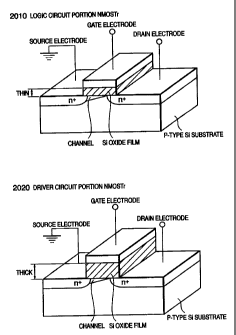
larger oxide film thickness TOX. 2010 and 2020 in
Fig. 2A are views schematically showing the NMOS
transistors of the logic and driver circuit portions
having different oxide film thicknesses.
In the first embodiment, as shown in 2020 of
Fig. 2A, the enhancement NMOS transistor which
constitutes the driver is formed with a gate oxide film
thickness of 70 nm. As shown in 2010 of Fig. 2A, the
enhancement NMOS transistor which constitutes the logic
circuit is formed with a gate oxide film thickness of
35 nm.
The oxide film thickness on the driver side is
larger than that of the transistor on the logic circuit
side. The threshold of a device formed under these
conditions is higher on the driver side by 1.5 V. When
a current of 140 mA per heater bit flows and heaters of
- 30 -
CA 02390750 2002-06-14
16 bits at maximum are instantaneously driven at the
same time, about 2.2 A is switched and noise of about
0.5 V is generated on the board. However, the driver
can stably operate without any malfunction.
Since the logic circuit is smaller in oxide film
thickness than the driver circuit, the threshold
becomes lower. The drivability of the element can be
improved even at a voltage of 3.3 V or lower supplied
from the apparatus main body. Even if the power supply
voltage is changed from 5 V to 3.3 V, the printing
apparatus can maintain a data transfer rate of 12 MHz
or higher and cope with high-speed printing.
According to the first embodiment, the oxide film
thickness of the driver portion can be set larger than
that of a conventional driver. The breakdown voltage
can also be increased in addition to the drivability.
Consequently, the current can be decreased, and any
loss and noise can be reduced.
<Second Embodiment: Channel Impurity Concentration>
The arrangement of a printhead board according to
the second embodiment is identical to that of Fig. 1A
in the first embodiment, and a detailed description
thereof will be omitted.
To prevent the malfunction of a heater element
and prevent an abnormal current from flowing, the
second embodiment controls the operating voltage
threshold of a transistor by using the channel impurity
- 31 -
CA 02390750 2002-06-14
concentration NA in equation (1) as a key parameter in
processing of step S1440 of Fig. 14. More
specifically, the operation threshold of an enhancement
NMOS transistor which constitutes a driver for driving
a heater, and the operation threshold of an enhancement
NMOS transistor which constitutes a logic circuit for
driving the driver are changed as follows. The channel
impurity concentration NA is changed to control the
channel impurity concentrations of the two transistors
so as to maintain the printing performance of the
ink-jet printing apparatus.
From the relation in equation (1), the threshold
Vth is higher for a higher channel impurity
concentration NA.
2030 and 2040 in Fig. 2B are views schematically
showing the NMOS transistors of the logic and driver
circuit portions having different channel
concentrations. In forming the gates of the
enhancement NMOS transistors of the driver and logic
circuit, the B ion implantation amount is controlled to
set the channel impurity concentration NA to be high
(heavy) for the transistor of the driver and low
(light) for the transistor of the logic circuit.
In this case, the channel impurity concentration
on the driver side is higher than that on the logic
circuit side. The threshold on the driver side is
higher by 1.5 V than that on the logic side. When a
- 32 -
CA 02390750 2002-06-14
current of 140 mA per heater bit flows and heaters of
16 bits at maximum are instantaneously driven at the
same time, about 2.2 A is switched and noise of about
0.5 V is generated on the board. However, the driver
can stably operate without any malfunction.
Since the logic circuit is lower in channel
impurity concentration than the driver circuit, the
threshold becomes lower. The drivability can be
improved even at a voltage of 3.3 V or lower supplied
from the apparatus main body. Even if the power supply
voltage is changed from 5 V to 3.3 V, the printing
apparatus can maintain a data transfer rate of 12 MHz
or higher and cope with high-speed printing.
The second embodiment can be achieved only by
controlling the channel concentration of the logic
circuit in a conventional manufacturing process. The
printhead board can be manufactured more easily than
the first embodiment.
<Third Embodiment: Oxide Film Thickness + Channel
Impurity Concentration>
To prevent the malfunction of a heater element
and prevent an abnormal current from flowing, the third
embodiment controls the operating voltage threshold of
a transistor by using control of the oxide film
thickness TOX and the channel impurity concentration NA
in equation (1) as key parameters in steps S1401 and
S1440 of Fig. 14. More specifically, the operation
- 33 -
I"'~ I! II ,
CA 02390750 2002-06-14
threshold of an enhancement NMOS transistor which
constitutes a driver for driving a heater, and the
operation threshold of an enhancement NMOS transistor
which constitutes a logic circuit for driving the
driver are changed as follows. The oxide film
thickness and channel impurity concentration NA are
changed in a superposition manner to control the
threshold voltages of the two transistors so as to
maintain the desired printing performance of the
ink-jet printing apparatus.
In Fig. 1B showing an ink-jet printhead board
according to the third embodiment, heater arrays 201B
including 512-bit heaters, driver arrays 202B having
drivers for driving the respective heaters, and logic
circuits 203B for driving the drivers are formed on a
single board 200B. Pads 204B for electrically
connecting the board to its outside are formed on the
board 200B. Ink supply ports 205B are formed at the
center of the board.
2050 and 2060 in Fig. 2C are views schematically
showing the NMOS transistors of the logic and driver
circuit portions having different oxide film
thicknesses and different channel impurity
concentrations.
In the third embodiment, as shown in 2060 of
Fig. 2C, the enhancement NMOS transistor which
constitutes the driver is formed with a gate oxide film
- 34 -
!; ~~ H 11
CA 02390750 2002-06-14
thickness of 70 nm and a high (heavy) channel impurity
concentration.
In equation (1), the operating voltage threshold
of the NMOS transistor is higher for a larger oxide
film thickness TOX. The threshold Vth increases as the
channel impurity concentration NA increases.
The oxide film thickness and channel impurity
concentration are selected and changed as parameters to
be controlled. The superposition effect of the two
parameters can change the thresholds of the respective
devices.
Accordingly, an element in which the driver has a
higher threshold than that adjusted by either parameter
can be formed. When a current of 140 mA per heater bit
flows and heaters of 32 bits at maximum are
instantaneously driven at the same time, about 4.4 A is
switched and noise of about 1.0 V is generated on the
board. However, the driver can stably operate without
any malfunction.
The enhancement NMOS transistor which constitutes
the logic circuit is formed with a gate oxide film
thickness of 10 nm and a lower channel impurity
concentration. In this case, an element with a lower
threshold than that adjusted by either parameter can be
formed. The drivability of the element can be improved
even at a power supply voltage of 2 V or lower supplied
from the apparatus main body. The printing apparatus
- 35 -
{,,,, ,I I {I ;
CA 02390750 2002-06-14
can maintain a data transfer rate of 20 MHz to 30 MHz
and cope with high-speed printing.
The third embodiment separately sets the gate
oxide film thickness and channel impurity
concentration, and can set the threshold by an optimal
combination of them. This embodiment can provide a
board which can cope with high-speed printing while a
large current is stably switched.
As for the setting of the channel impurity
concentration, the impurity concentration at the
channel portion of the enhancement NMOS transistor
which forms the driver is set higher than that at the
channel portion of the enhancement NMOS transistor
which forms the logic circuit. Alternatively, the
impurity concentration at the channel portion of the
enhancement NMOS transistor which forms the driver may
be set lower than that at the channel portion of the
enhancement NMOS transistor which forms the logic
circuit. This setting is also included in the third
embodiment.
In the above embodiments, droplets discharged
from the printhead are ink, and a liquid stored in the
ink tank is ink. The content of the ink tank is not
limited to ink. For example, the ink tank may contain
a processing solution to be discharged onto a printing
medium in order to increase the fixing properties,
water resistance, or quality of a printed image.
- 36 -
I~ LI II
CA 02390750 2002-06-14
The above embodiments can employ an element such
as a piezoelectric element or heat generation element
as an energy generation element for discharging ink.
Of ink-jet printing systems, the embodiments can adopt
a system which comprises a means (e.g., an
electrothermal transducer) for generating heat energy
as energy utilized to discharge ink and causes a state
change of ink by the heat energy. This ink-jet
printing system can increase the printing density and
resolution.
As a representative arrangement or principle, the
present invention preferably uses the basic principle
disclosed in, e.g., U.S.P. No. 4723129 or 4740796.
This system is applicable to both a so-called on-demand
apparatus and continuous apparatus. The system is
particularly effective in an on-demand apparatus
because of the following reason. At least one driving
signal which corresponds to printing information and
gives a rapid temperature rise exceeding nuclear
boiling is applied to an electrothermal transducer
which corresponds to a sheet or liquid channel holding
a liquid (ink). This signal causes the electrothermal
transducer to generate heat energy and causes film
boiling on the heat acting surface of a printhead.
Consequently, a bubble can be formed in the liquid
(ink) in one-to-one correspondence with the driving
signal.
- 37 -
I I' ;I i 41 ~
CA 02390750 2002-06-14
Growth/shrinkage of this bubble discharges the
liquid (ink) from an orifice to form at least one
droplet. This driving signal is more preferably a
pulse signal because growth and shrinkage of a bubble
are instantaneously appropriately performed. Discharge
of the liquid (ink) with high response is achieved.
The above-described embodiments can employ an
element such as a piezoelectric element or heat
generation element as an energy generation element for
discharging ink. Of ink-jet printing systems, the
embodiments can adopt a system which has a means (e.g.,
electrothermal transducer) for generating heat energy
as energy utilized to discharge ink, and changes the
ink state by the heat energy. This ink-jet printing
system can realize high-density, high-precision
printing.
The arrangement of the printhead can be a
combination (linear liquid channel or right-angle
liquid channel) of orifices, liquid channels, and
electrothermal transducers disclosed in the
specifications described above. The present invention
also includes arrangements disclosed in U.S.P.
Nos. 4558333 and 4459600 in each of which the heat
acting surface is placed in a bent region. The present
invention also uses an arrangement based on Japanese
Patent Laid-Open No. 59-123670 in which a common slot
is used as a discharge portion of a plurality of
- 38 -
~ I I i II ~
CA 02390750 2002-06-14
electrothermal transducers or Japanese Patent Laid-Open
No. 59-138461 in which an opening for absorbing the
pressure wave of heat energy is opposed to a discharge
portion.
A full line type printhead having a length
corresponding to the width of the largest printing
medium printable by a printing apparatus can have a
structure which meets this length by combining a
plurality of printheads as disclosed in the
above-mentioned specifications or can be a single
integrated printhead.
It is possible to use not only a cartridge type
printhead, explained in the above embodiments, in which
ink tanks are integrated with a printhead itself, but
also an interchangeable chip type printhead which can
be electrically connected to an apparatus main body and
supplied with ink from the apparatus main body when
attached to the apparatus main body.
Adding a recovering means or preliminary means
for a printhead to the arrangement of the printing
apparatus described above is preferable because
printing can further stabilize. Practical examples of
the additional means for a printhead are a capping
means, a cleaning means, a pressurizing or drawing
means, and an electrothermal transducer or another
heating element, or a preliminary heating means
combining them. A predischarge mode for performing
- 39 -
~ 3i i~l 41 3
CA 02390750 2002-06-14
discharge different from printing is also effective to
perform stable printing.
The printing mode of the printing apparatus is
not restricted to a printing mode using only a main
color such as black. The apparatus can have at least a
composite color mode using different colors and a full
color mode using mixed colors, regardless of whether a
printhead is an integrated head or a combination of a
plurality of heads.
The above embodiments are explained assuming that
ink is a liquid. However, it is possible to use ink
which solidifies at room temperature or less but
softens or liquefies at room temperature. In inkjet
systems, the general approach is to perform temperature
control such that the viscosity of ink falls within a
stable discharge range by adjusting the temperature of
the ink itself within the range of 300C to 700C. Hence,
ink needs only to be a liquid when a printing signal
used is applied to it.
To positively prevent a temperature rise caused
by heat energy by positively using this temperature
rise as energy of the state change from the solid state
to the liquid state of ink, or to prevent evaporation
of ink, ink which solidifies when left to stand and
liquefies when heated can be used. The present
invention is applicable to any ink which liquefies only
when heat energy is applied, such as ink which
- 40 -
1 I1;I ;I 4 41 ;
CA 02390750 2002-06-14
liquefies when applied with heat energy corresponding
to a printing signal and is discharged as liquid ink,
or ink which already starts to solidify when arriving
at a printing medium.
As described in Japanese Patent Laid-Open
No. 54-56847 or 60-71260, this type of ink can be held
as a liquid or solid in a recess or through hole in a
porous sheet and opposed to an electrothermal
transducer in this state. In the present invention,
executing the aforementioned film boiling scheme is
most effective for each ink described above.
Furthermore, the printing apparatus according to
the present invention can take the form of any of an
integrated or separate image output terminal of an
information processing apparatus such as a computer, a
copying apparatus combined with a reader or the like,
and a facsimile apparatus having a
transmission/reception function.
As has been described above, the threshold of a
transistor on the driver side is higher than that of a
transistor on the logic circuit side in the ink-jet
printhead board, ink-jet printhead, and ink-jet
printing apparatus according to the present invention.
Even when a voltage supplied from the printing
apparatus main body is 3.3 V or lower, a stable
operation can be realized without any malfunction of
the driver even under this voltage condition.
- 41 -
, ; I l~ll il IiI i
CA 02390750 2002-06-14
The drivability of the element can be improved.
Even if the power supply voltage is changed from 5 V to
3.3 V, the printing apparatus can maintain a high data
transfer rate and cope with high-speed printing.
As many apparently widely different embodiments
of the present invention can be made without departing
from the spirit and scope thereof, it is to be
understood that the invention is not limited to the
specific embodiments thereof except as defined in the
claims.
- 42 -