Note: Descriptions are shown in the official language in which they were submitted.
CA 02391331 2002-O1-23
WO 01/99114 PCT/USO1/40736
Description
REFERENCE CELL FOR HIGH SPEED SENSING
TN NON-VOLATILE MEMORIES
FIELD OF THE INVENTION
The present invention relates to sense amplifi-
ers for use with nonvolatile seifiiconductor memories.
More specifically, it relates to the structure of a ref-
erence memory cell used in establishing a reference volt-
age for a sense amplifier.
BACKGROUND ART
Within a memory IC, sense amplifiers are used
to read data from a target memory cell within a memory
array. These amplifiers are typically categorized as
single-ended sense amplifiers or differential sense am-
plifier. Single-ended sense amplifiers are commonly used
in memories having a single-bit per memory cell. Exam-
ples of single-bit per cell memories are EEPROM and Flash
EPROMs. These single-bit per cell memories store only
one of the true value or compliment value of a datum item
in each memory cell. This is in contrast to dual-bit per
cell memories such as SRAMs, which store both the true
and complement value of a datum item in each memory cell.
Having both the true and complement value of a datum item
within each memory cell facilitates and speeds up the
reading of a memory cell since one can identify the
stored datum item by simultaneously accessing both true
and complement bits and simply determining which has the
higher voltage potential. Stated more clearly, SRAMs use
differential amplifiers to read each memory cell, and
identify the logic state stored within a memory cell as
soon as the direction of the voltage imbalance, represen-
tative of the true and complimentary data stored within
the memory cell, is determined. Since single-bit per
cell memories do not have the luxury of knowing the com-
pliment of the stared datum item, their single-ended
CA 02391331 2002-O1-23
WO 01/99114 PCT/USO1/40736
_2_
sensing circuitry requires a different, and more criti-
cally balanced approach.
Use of a differential sense amplifier in a
nonvolatile memory would provide a big boost in reading
speed, but would require two memory storage devices per
memory cell, one for the true data and another for the
complement data. This would reduce the memory capacity
at least by 50%. It is more likely that the reduction
would be much greater because of the need to accommodate
additional bitlines, equalization circuitry, more complex
program and erase circuitry, and other circuitry required
to implement a dual-bit per memory cell architecture.
Therefore, nonvolatile memories generally use single-
ended sense amplifiers.
With reference to Fig. 1, a single-ended sens-
ing circuit 12 suitable for use with a single-bit memory
cell is shown 14. Target single-bit memory cell 14 is
depicted as a single floating gate transistor 16. Sens-
ing circuit 12 determines the logic state stored within
target memory cell 14 by sensing a potential difference
between a sense line 18 coupled to target memory cell 14
and a reference line 20 coupled to a reference memory
cell 22. The potential of sense line 18 is dependent on
the logic state, high or low, of the datum stored within
target memory cell 14. Typically, if the potential of
sense line 18 is higher than that of reference line 20,
then target memory cell 14 is read as having a logic low
state, and if the potential of sense line 18 is lower
than reference line 20, then target memory cell 14 is
read as having a logic high state. Therefore, it is
important that the voltage potential of reference line 20
be maintained at a value intermediate the logic high and
logic low voltage potentials of target cell 14.
At first glance, it would appear that the ref-
erence voltage on line 20 could be produced with a con-
stant voltage generator, but this is not preferred. The
potential at sense line 18 is affected not only by the
potential at the gate of floating gate transistor 16, but
CA 02391331 2002-O1-23
WO 01/99114 PCT/USO1/40736
-3-
also by the architecture of the memory. The capacitive
loads of target memory cell 14 depend on its physical
structure and on its location within a larger memory
array. These capacitive loads, in turn, affect the cur-
s rent sourcing capability of target memory cell 14 and
thereby the potential at sense line 18.
Therefore, an effort is made to help reference
line 20 reflect these capacitive loads in order to better
track the logic high and logic low voltages of target
memory cell 16. A typical method of tracking these ef-
fects on the logic high and logic low voltages of a tar-
get memory cell is to use another memory cell, i.e. a
reference memory cell 22, to produce the voltage poten-
tial for reference line 20. The idea is that since the
reference memory cell 22 has a similar structure as tar-
get memory cell 14, its behavior will be similar to that
of target cell 14. The potential of reference line 20 is
therefore dependent on the current sourcing value of
reference cell 22.
Various methods of using a reference cell for
producing the reference voltage for use with a single-
ended sensing circuit are known in the art. Some of
these methods are discussed in U.S. Pat. No. 5,572,474 to
Sheen et al., U.S. Pat. No. 5,608,679 to Medlock et al.,
and 5,642,308 to Yoshida.
Applicants have found, however, that existing
methods of generating a reference voltage on reference
line 20 are not stable over the life of the memory IC.
This is in part due to reference cell 22 using a floating
gate transistor 26 to produce the reference voltage.
Although using a floating gate transistor 26 within ref-
erence cell 22 is advantageous because it provides a
better balance with the floating gate transistor 16 of
target memory cell 14, floating gate transistor 26 intro-
duces additional problems that may complicate generating
an accurate reference voltage on reference line 20.
Since the threshold voltage of reference cell
22 should not changed, reference cell 22 is isolated from
CA 02391331 2002-O1-23
WO 01/99114 PCT/USO1/40736
-4-
program and erase circuitry used in altering the state of
the storage memory cells 14 in a main memory array.
Reference memory cells, in general, are constructed with
no charge on their floating gate 28, and the charge level
on their floating gate 28 is not intended to change since
they are not connected to any programming or erasing
circuitry. If desired, the threshold voltage level of
reference cells may be adjusted by adjusting the sub-
strate doping concentration of their channel region.
Unfortunately, there are several factors that
can alter the charge level of a reference cell's floating
gate 28. Floating gate transistors, in general, are
susceptible to read disturb problems that can change the
amount of charge on a reference cell's floating gate 28,
which results in a change in its threshold voltage. This
can result in a change in the cell's reference current
value, which in turn changes the voltage value of refer-
ence line 20. Due to the critical balancing of the sens-
ing circuit 12, a voltage change in sense line 20 can, at
best, slow down sensing circuit 12, and at worst, cause
it to read erroneous data.
Additionally, Applicants have identified an-
other source of error associated with the use of a float-
ing gate reference cell 22. The manufacturing of nonvol-
able memory ICs often requires the use of plasmas.
Plasma has an intrinsic electric charge associate with it
that will typically alter the charge on the floating gate
of a nonvolatile memory cell during the manufacturing
process. To accommodate for this change in the floating
gate charge, the main memory array is typically subjected
to an erase sequence at the end of the manufacturing
process. However, since reference cell 22 is isolated
from the main memory's program and erase circuitry, it is
not erased in this erase sequence and its floating gate
is not brought to a neutral position. One method of
addressing this problem is to subject the entire memory
IC to ultra violet, UV, light for a predetermined period
of time at the end of the manufacturing process. Expo-
CA 02391331 2002-O1-23
WO 01/99114 PCT/USO1/40736
-5-
sure to UV light can erase reference cell 22, but one
cannot be certain that reference cell 22 is fully erased.
As a result, sense amplifier 12 must accommodate for such
variations, which necessarily slows it down.
As the density of nonvolatile memories contin-
ues to increase and their speeds requirements continue to
rise, every factor affecting the speed performance be-
comes more critical. It is an object of the present
invention to provide a faster, and more process insensi-
tine, sense amplifier.
It is another object of the present invention
to generate a reference voltage for use with a sense
amplifier that is not affected by threshold voltage
changes in the sense amplifier's reference cell, but
which still accurately tracks variations in a target
memory cell within the main memory array.
It is still another object to provide a refer-
ence cell that compensate for layout variations in a
compact EEPROM memory structure.
SUMMARY OF THE INVENTION
The above objects are met in a single-ended
sense amplifier having a reference cell circuit whose
structure mirrors that of the main memory array, but
which does not rely on accurate measures of charge stored
within a floating gate to establish a reference voltage.
The sense amplifier's reference voltage is dependent on
the level of current sourced by its reference cell. This
level of current is in turn dependent on the reference
cell's threshold voltage, structural characteristics and
physical layout. Since the structure of the reference
cell is similar to that of the target memory array, the
reference voltage tracks changes over the life of the
target memory array. To better track the physical layout
of a target memory cell within the main memory array, the
present reference cell circuit include two different
reference cell layouts. A first reference cell layout
corresponds to the layout of a target memory cell in an
CA 02391331 2002-O1-23
WO 01/99114 PCT/USO1/40736
-6-
even numbered row, and a second reference cell layout
correspond to the layout of a target memory cell in an
odd numbered row. This permits even closer tracking of
cell layout variations of target cell within the main
memory array.
A reference cell's threshold voltage, and
thereby its current sourcing capability, is also depend-
ent on the amount of charge on its floating gate. As
explained above, the charge on the floating gate estab-
fishes a threshold voltage for a memory cell, which de-
termines how much current it sources in response to a
voltage applied at its control gate. Applicants have
found, however, that reliance on the floating gate to
establish the threshold voltage of the reference cell can
introduce unexpected errors.
During the manufacture of a memory IC, it is
often required that the memory IC be submitted to a
plasma process step. This, for example, may be part of a
plasma etchant step. Plasma has an associated charge,
and the floating gates of all floating gate transistors
will be partly charged during a plasma step. This does
not severely affect the main array since it generally
undergoes an erase sequence during initial testing of the
memory IC, which removes any accumulated charge from
their respective floating gates. The reference cells,
however, do not under this erase step. Indeed, memory
IC's typically do not have erase circuitry coupled to the
reference cells. To reduce the charge trapped within the
floating gates after manufacture, the memory IC is typi-
cally subjected to an ultra violet erase step. Ideally,
the W light should remove the charge within each memory
cell and bring all floating gate within an IC to a known
charge state. This is critical for the reference cell
since it must generate a known, and precisely controlled
current. Any variation from the expected value will slow
down the sensing of a cell since the tolerance margins
would have to be relaxed. It has been found, however,
that not all referenced cells are fully erased during
CA 02391331 2002-O1-23
WO 01/99114 PCT/USO1/40736
this W light erase step, which prevents the IC from
having its read margins tightened and thereby its read
access time shorten.
Even if the charge in a the reference cell can
be initiated to known low values, the charge on the
floating gate is prone to vary over the life of the mem-
ory. In other words, the charge on the reference cell
will change over time as a result of normal read opera-
tions. This is due to various phenomena, such as an
error known as read disturb, which can cause a small
change in the amount of charge stored within a floating
gate by virtue of repeated read operations. Since the
reference cell is read every time any memory cell within
the main memory array is read, the reference cell is more
susceptible to read disturb problems.
The present invention addresses both of the
above listed, floating gate related, sources of error by
not allowing the reference cell's floating gate to float.
The reference cell's control gate is connected to the
cell's floating gate. This permits the present invention
to eliminates any errors resulting from charge variations
on a floating gate. Furthermore, this also allows a
better control of the exact voltage coupling of the
floating gate to the control gate. Floating gate cells
typically having an ~5% to 90o coupling ratio between
their control gate and their floating gate, and this
coupling ratio cannot be controlled to an exact value.
Additionally, the effective coupling margin is likely to
change over the life the cell as the charge on the float-
ing gate varies. By offering a precise coupling ratio of
1000, the present invention can further tighten the oper-
ating margins of the memory IC and thereby increase its
speed.
Since the amount of charge on the floating gate
is controlled by a direct line from its control gate, it
is not susceptible to charge buildup or charge leakage on
the floating gate. Thus, the present reference cell is
unaffected by charge buildup caused by plasma steps in
CA 02391331 2002-O1-23
WO 01/99114 PCT/USO1/40736
_g_
the manufacturing process. This also makes the reference
memory cell resistant to other floating gate related
errors such as read disturb and aging. The amount of
charge on the floating gate is directly adjusted by a
digitally controlled, constant reference voltage source
coupled to the control gate of the reference cell's con-
trol gate. This permits the present invention to tighten
the operating margins even more, resulting in greater
speed gains.
Use of a reference cell having its control gate
tied to its floating gate allows the present invention to
focus on tracking the architectural layout of the target
memory cells within the main memory array. The reference
cell of the present invention tracks a target memory
cell's structure, ion implantation profile, layout, etc.
to assure an accurate comparison for read operations,
without being prone to the errors associated with the use
of a floating gate structure.
Preferably, the reference Cell circuitry of the
~0 present sense amplifier consists of two reference cells
to mimic two floating gate transistors on adjacent rows
of a target memory array sharing the same bitline and the
same source line. It has been found that the memory
array layout can affect the reading of a targeted memory
cell. A first target memory cell lying within a first
row may produce a different voltage on its bitline, than
a second target memory cell having the same stored data
value and coupled to the same bit Line but lying on an
adjacent row. This is in part due to the physical layout
orientation of the two cell which causes them "to see"
different Capacitive load levels. To compensate for
this, the layout of the two reference floating gate tran-
sistors of the present invention is constructed in a
manner corresponding to the memory layout of a target
memory cell on an even number row Coupled to an adjacent
target memory cell in an odd number row. The digitally
controlled constant reference voltage source of the pres-
ent invention can determine whether an even number row or
CA 02391331 2002-O1-23
WO 01/99114 PCT/USO1/40736
-9-
an odd number row is being addressed, and activate only
the reference floating gate transistor having a layout
corresponding to the appropriately targeted even or odd
numbered row. This permits the present invention to
better match voltage variations within the main memory
array and thereby further tighten operating margins to
achieve higher speeds.
BRIEF DESCRIPTION OF THE DRAWINGS
Fig. 1 is prior art view of a single-ended
sense amplifier and a reference cell.
Fig. 2 is a flash memory structure using a
sensing scheme in accord with a first embodiment of the
present invention.
Fig. 3 is a plot of voltage potentials on a
sense line and on a reference line.
Fig. 4 is plot of voltage potentials on a sense
line and reference line having tighter tolerance levels
that shown in Fig. 3.
Fig. 5 is a first sample layout of an EEPROM
main memory array in accord with the present invention.
Fig. 6 is a second sample layout of an EEPROM
main memory array in accord with the present invention.
Fig. 7 is a reference cell in accord with a
second embodiment of the present invention.
Fig. 8 is a control voltage generator for a
reference in accord with the present invention.
Fig. 9 is a layout view of a reference cell in
accord with the second embodiment of the present inven-
tion.
Fig. 10 is a detailed view of a sense amplifier
in accord with the present invention.
BEST MODE FOR CARRYING OUT THE INVENTION
With reference to Fig. 2, a sample view of a
partial flash memory 11 in accord with the present inven-
tion is shown. The sample view shows a main memory array
13 coupled through a partial y-decoder 15 to a single-
CA 02391331 2002-O1-23
WO 01/99114 PCT/USO1/40736
-10-
ended sensing circuit 17. Memory array 13 consists of a
plurality of memory cells C00 to Cnm arranged in n rows
and m columns. An X-address permits each row of memory
cells to be individually addressed by selecting, i.e.
actuating, a corresponding wordline, XO to Xn. Simi-
larly, each column of memory cells may be uniquely iden-
tified by a Y-address that selects a corresponding
bitline BO to Bm. An individual memory cell is selected
if it lies at the intersection of a selected wordline and
a selected bitline. For example, if it were desired to
select memory cell Cn1 for a read operation, then
wordline Xn, corresponding to row n, and bitline B1,
corresponding to column 1, would be selected. To
select row n, a read voltage, of for example 5V, is ap-
plied to wordline Xn while all other wordlines received
OV. The read voltage applied to wordline Xn is applied
to all memory cells within the row defined by wordline
Xn, i.e. memory cells Cn0 to Cnm. Anyone of memory cells
Cn0 to Cnm within the selected row may respond to the
applied read voltage by coupling its drain to ground,
which would consequently couple its corresponding bitline
BO to Bm to ground. As a result, multiple bitlines BO to
Bm may be coupled to ground during a read operation.
Single-ended sensing circuit 17 determines the
logic level of the data stored within a selected memory
cell by determining if the target cell's corresponding
bitline is coupled to ground during the read operation.
Typically, a bitline coupled to ground is indicative of a
logic,l and a bitline isolated from ground is indicative
of a logic 0. Therefore, in order to read memory cell
Cnl, flash memory 11 must determine if Cn1's correspond-
ing bitline, B1, is coupled to ground. Tn order to do
this, it must ignore the state of all other bitlines,
Partial y-decoder 15 isolates the bitline corresponding
to target memory cell Cnl, bitline B1 in this case, from
all other bitlines and couples it to an intermediate node
19, which is an input to single-ended sensing circuit 17.
Y-select lines YO to Ym activate one of Y-decode transis-
CA 02391331 2002-O1-23
WO 01/99114 PCT/USO1/40736
-11-
for Ty0 to Tym. By actuating only Y-select line Y1, only
the corresponding bitline, i.e. B1, is coupled to inter-
mediate node 19.
A memory cell, C00 to Cnm, couples its corre-
sponding bitline, BO to Bm, to ground if its threshold
voltage is below the read voltage applied to its corre-
sponding wordline XO to Xn. Otherwise, the memory cell
C00 to Cnm remains off and its corresponding bitline
remains isolated from ground. Thus, logic high and low
data is stored in a memory cell by adjusting the memory
cell's threshold voltage. This is done by adding or
removing charge from the floating gate of the non-vola-
tile floating gate transistor within the memory cell. To
store a logic high, i.e. logic 1, charge is removed from
floating gate 21, which lowers its threshold voltage
below the read voltage. Conversely, to store a logic
low, i.e. logic 0, charge is added to floating gate 21,
which raises it threshold voltage above the read voltage.
Single-ended sensing circuit 17 includes a
differential amplifier, typically referred to in the art
as a sense amplifier 23 having two inputs, a sense line
and a reference line 27. Since sense line 25 is cou-
pled to a pull-up device represented as pull-up resistor
33. Sense line 25 is also coupled to intermediate node
25 19 through a pass NMOS device 31. Intermediate node 19
is additional coupled to VCC via a pull-up NMOS device
35. If intermediate node 19 is not coupled to any
bitline, BO to Bm, then it will be pulled up toward a
predetermined reference high voltage through pull-up NMOS
device 35 and pull-up resistor 33.
A bias voltage generator 37 determines the
actual reference high voltage of intermediate node 19.
The source electrode of an NMOS transistor cannot rise
higher than one threshold voltage below the potential
applied to its control gate. Since the output of bias
voltage generator 37 is coupled to the control gate of
both NMOS device 31 and 35 arid their respective source
electrodes are coupled to intermediate node 19, the high-
CA 02391331 2002-O1-23
WO 01/99114 PCT/USO1/40736
-12-
est potential intermediate node 19 can reach is at most
one threshold voltage below the output of bias voltage
generator 37.
Whenever partial y-decoder 15 couples a
bitline, BO to Bm, to intermediate node 19, the higher
capacitive value of the bitline causes the voltage at
intermediate node 19 to be momentarily pulled down.
Pull-up NMOS device 35 and pull-up resistor 33 then start
raising the voltage of intermediate node 19. The final
voltage value of intermediate node 19 depends on the
datum stored within the target memory cell. If the tar-
get memory cell has a logic 0, and thus remains off in
response to an applied read voltage, then the correspond-
ing bitline will be isolated from ground and intermediate
node 19 will rise to the aforementioned predetermined
voltage. On the other hand, if the targeted memory cell
has a logic 1, and thus turns on in response to an ap-
plied read voltage, then the corresponding bitline will
be coupled to ground through the memory transistor and
the potential of intermediate node 19 will reach a lower
potential. Since sense line-25 is coupled to intermedi-
ate node 19 through NMOS device 31, its potential Vsense
tracks that of intermediate node 19.
With reference to Fig. 3, sample Vsense volt-
ages corresponding to the reading of a logic 0 and a
logic 1 are shown. Initially, Vsense is pulled low when
intermediate node 19 is first coupled to a selected
bitline. If the targeted memory transistor has a logic
1, then Vsense will rise to a maximum logic low poten-
tial, VLL~, but remain below reference voltage Vref. If
the targeted memory transistor has a logic 0, then Vsense
will rise to a maximum logic high voltage VLH~ that is
above reference voltage Vref. In this manner, sense
amplifier 23 can determine the contents of a targeted
memory transistor.
It should be noted that Vref is defined by a
maximum error margin VrefM. As explained above, reference
voltage Vref applied to sense amplifier 23 is prone to
CA 02391331 2002-O1-23
WO 01/99114 PCT/USO1/40736
-13-
vary for a variety of reasons. Therefore, the value of
Vref may not be assumed to be absolute and must instead
be defined by a margin of error VrefM. As a result, sense
amplifier 23 may not identify a logic 0 signal until
Vsense has been given enough time to rise above Vref's
margin of error. The time required for sense amplifier
23 to determine the logic state of the targeted memory
transistor is labeled tsense in Fig. 3.
As seen, tsense is the sum of three components,
~ tLL, tmargin~ and t~P. The tLL time is the maximum time
required for a logic low signal to reach its highest
potential VLL~. After this, sense amplifier 23 must
wait for the time, tmargin~ that it would take a logic high
signal to rise above Vref's error margin, VrefM. Fi-
nally, t~P, is the time required for sense amplifier 23
to make a decision about the voltage value of Vsense
relative Vref . Times tLL and t~P are fixed, but time tmargin
may be reduced by reducing Vref's margin of error, VrefM.
With reference to Fig. 4, an example of a
shorter sense time tsense resulting from a reduced margin
of error VrefM is shown. All elements in Fig. 4 similar
to those of Fig. 3 are identified with similar reference
characters and are explained above. In the present exam-
ple, the error margin VrefM of reference voltage Vref is
reduced by about 15o to form new VrefM' in Fig. 4. Be-
cause of the logarithmic nature of the rise time of
Vsense, this 15% reduction in the error margin of refer-
ence voltage Vref, results in almost a 70o reduction in
the tmargin~ the time that the sense amplifier must wait for
a logic high Vsense signal to rise from VLLMa,~ to above
the error margin VrefM'. In the present example, the 15%
reduction in VrefM also resulted in a 20% reduction in
the overall tsense time required for sense amplifier 23
to compare Vsense to Vref. Thus, even small improvements
in Vref's error margin can result in sizable gains in
speed.
Returning to Fig. 2, Vref is the potential of
reference line 27. As explained above, it is important
CA 02391331 2002-O1-23
WO 01/99114 PCT/USO1/40736
-14-
that Vref track variations in main memory array 13.
Therefore, most of the circuit elements in the read path
of memory array 13 are reproduced in the path for gener-
ating the reference voltage. Reference line 27 is shown
coupled to a second pull-up resistor 43 and coupled to a
second intermediate node 39 via a second NMOS pass tran-
sistor 41. Second intermediate node 39 is coupled to Vcc
via a second pull-up NMOS device 45. A reference memory
cell 47 is coupled through a select transistor 49 to
second intermediate node 39. This structure mirrors the
structure used to address main memory array 13 through y-
decoder 15. The main difference in that the structure of
reference memory cell 47 is not the same as that of any
of memory cells C00 to Cnm in main memory array 13.
Reference cell 47 does not include a memory
transistor. Rather, it includes a reference transistor
51 having a structure similar to the memory transistors
within memory cells C00 to Cnm in main memory array 13,
but reference transistor 51 does not have a floating
gate. The control gate of reference transistor 51 is
broken into two parts, a first part 55 is in direct con-
tact with a control line 57 and a second part 53 is in-
terpose between the first part 55 and the channel of
reference transistor 51. This second part 53 of the
control gate is separated from the first part 55 and from
the transistor channel by insulative oxide. The dimen-
sions of the first part 55 are preferably the same as the
dimensions of the control gates of memory cells C00 to
Cnm, and the dimensions of the second part 53 are is
preferably the same as the floating gates 21 of memory
cells C00 to Cnm. Also, the oxide separating the second
part 53 from the first part 55 is preferably the same as
the inter-gate oxide separating the floating gate 21 from
the control gate within memory cells C00 to Cnm. Lastly,
the dimensions of the oxide separating the second part 53
of the control gate from the channel region of reference
transistor 51 is preferably the same as the tunneling
oxide separating the floating gate 21 of memory cells C00
CA 02391331 2002-O1-23
WO 01/99114 PCT/USO1/40736
-15-
to Cnm from their respective channel regions. Structur-
ally, reference transistor 51 looks like a floating gate
transistor within any of memory cells C00 to Cnm and has
similar dimensions, but reference transistor 51 addition-
s ally has a coupling arm 59 connecting the first part 53
of its control gate to the second part 55 of its control
gate.
In this manner, the second part 53 of the con-
trol gate, which would represent a floating gate in mem-
ory cells C00 to Cnm is not allowed to float. Therefore,
reference cell 47 is not susceptible to voltage threshold
variations resulting from the alteration of charge on the
second part 53 of its control gate. This is because
charge cannot be stored on interpose part 53 of the ref-
erence transistor's control gate and therefore its
threshold voltage cannot be altered in this manner. As a
direct result, the present invention is not susceptible
to reference voltage Vref variations resulting from the
use of plasma during its manufacturing process. Again,
this is due to the potential of the second, interpose
part 53 being directly controlled by the first part 55 of
the control gate. Additionally, the present invention
overcomes the problem of not having absolute control over
the coupling ration between the control gate and floating
gate of a prior art reference cell, as described above.
In the present case, the second interpose part 53 has a
100% coupling ration to the first part 55 of the control
gate through connecting arm 59. With these sources of
error eliminated, the margin of error of Vref can be
reduced resulting in faster reading speeds.
In Fig. 2, main memory array 13 is shown having
a structure typical in EPROM and Flash EPROM memories,
but the structure of memory array 13 could be replaced
with that of an EEPROM. Fig. 5, for example, shows a
memory array 13 having an EEPROM memory array arrange-
ment. As it would be understood, the memory array 13 of
Fig. 5 would typically take the place of memory array 13
of Fig. 2. Therefore, all elements in memory array 13 of
CA 02391331 2002-O1-23
WO 01/99114 PCT/USO1/40736
-16-
Fig. 5 similar to those of memory array 13 of Fig. 2 are
given similar reference characters and are explained
above. In the present case,' each cell C00 to Cnm con-
sists of a select transistor 61 in series with a floating
gate memory transistor 63. Each wordline XO to Xn is
coupled to the control gate of both the select 61 tran-
sistor and floating gate transistor 63 of each memory
cell C00 to Cnm within a corresponding row. Each row has
a separate ground source line SO to Sn, and source elec-
trode of all floating gate transistors 63 within each row
are coupled to their corresponding source line.
A reference cell in accord with the present
invention would match the architecture of any of memory
cells C00 to Cnm within memory array 13 of Fig. 5 with
the exception that the floating gate would be shorted to
the control gate. In effect, reference cell 47 of Fig. 2
would be replaced with a two transistor reference cell.
The two transistor reference cell would follow the struc-
ture of reference cells C00 to Cnm in Fig. 5 and have a
select transistor in series with a two-gate transistor
similar to that the select transistor 61 in series with
floating gate transistor 63 of main memory array 13. The
main difference would be that in the reference cell, the
floating gate would have a coupling arm connecting it to
its respective control gate, in a manner similar to ref-
erence transistor 51 of Fig. 2. Although the architec-
ture of Fig. 5 is easily integrated into the architecture
of Fig. 2, it is not the most convenient since it re-
quires much more space in an IC.
A more compact memory array architecture suit-
able for an EEPRQM memory is shown in Fig. 6. All ele-
ments in Fig. 6 similar to those of Fig. 5 are given
similar reference characters and are explained above.
The structure of Fig. 6 requires only one source line SO
per pair of wordlines X0, X1. Additionally, memory cells
in adjacent rows share drain connections to a common
bitline. This reduces the number of required contacts
CA 02391331 2002-O1-23
WO 01/99114 PCT/USO1/40736
-17-
per memory cell and thereby reduces the size of the over-
all memory array 13.
This compact structure, however, complicates
the use of the reference memory cell used within the
sensing circuit 17. As explained above, it is desirable
that the reference cell match the general structure of
the memory cells within the main memory array 13. Al-
though the reference cell would still require a select
transistor in series with a floating gate memory transis-
tor, as was required with the structure of Fig. 5, Appli-
cants have found that such a structure does not provide
the best component matching and does not provide for the
most reduction of the error margin of reference voltage
Vref .
The layout of a memory array can greatly affect
its capacitance distribution, and thus its behavior.
Simply using a two-transistor memory cell within the
reference cell in a memory using the array structure 13
of Fig. 6 would not assure that the reference voltage
Vref would accurately track changes in the main array 13.
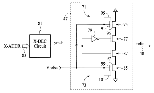
With reference to Fig. 7, a reference cell 47
in accord with a second embodiment of the present inven-
tion and suitable for the memory array layout of Fig. 6
is shown. Reference cell 47 includes first and second
sub-components 73 and 71, only one of which is active
during each read operation. First sub-component 73 con-
sists of a first select device 87, implemented as an nmos
switch transistor, in series with a first reference tran-
sistor 85. First select device 87 and first reference
transistor 85 are connected in series between an output
lead, refin, 48 and ground. Second sub-component 71
consists of a second select device 77, implemented as an
nmos switch transistor, in series with a second reference
transistor 75. Second select device 77 and second refer-
ence transistor 85 are connected in series between output
lead 48 and ground.
A control line ymsb selectively activates one
of first and second sub-components 71 and 73. Control
CA 02391331 2002-O1-23
WO 01/99114 PCT/USO1/40736
-18-
signal ymsb is coupled through an inverter 79 to the
control gate of second select device 77, and ymsb is
coupled directly to the control gate of first select
device 87. If control signal ymsb has a logic high, then
first sub-circuit 73 is activated, and if control signal
ymsb has a logic low, then second select sub-circuit 71
is selected. The logic'state of control signal ymsb is
directly related to the whether an even or odd numbered
row is selected within main memory array 13.
An X-decoding circuit 81 receives X-address bus
83, which carries the address of the row being addressed
within main memory 13. X-decoder circuit 81 may be the
main X-address decoder that is used to select a row of
memory cells within main memory array 13, or it may be a
second X-address decoder especially used for selecting
one of first and second sub-circuits 71 and 73. Alterna-
tively, signal ymsb may be tapped off of the least sig-
nificant bit of the x-address since a zero on this bit
would be indicative of an even numbered row and a 1 would
be indicative of an odd numbered row. In this case, the
x-address itself would control the reference cell 47.
If X-decoder 81 is part of the main X-address
decoder, then X-decoding circuitry 81 includes an X-
predecoder in series with an X-decoder, and together they
select a single wordline within main memory array 13. In
this case, X-decoding circuit 81 also issues a signal on
control line ymsb. In this presently preferred embodi-
ment, if X-address bus 83 indicates an even numbered row,
then a logic low will be placed on control line ymsb and
second sub-circuit 71 will be selected. Conversely, if
X-address bus 83 indicates an odd numbered row, then a
logic high will be placed on control line ymsb and first
sub-circuit 73 will be selected. Since X-decoding cir-
cuit 81 will typically know if an odd or even numbered
row is being address after its X-predecoder state and
before its X-decoder, signal ymsb may be issued before
the exact address of the selected wordline has been fully
decoded. This permits the appropriate sub-component
CA 02391331 2002-O1-23
WO 01/99114 PCT/USO1/40736
-19-
within reference cell 47 to already be selected prior to
initiating reading of a target memory cell.
In this manner, the~present reference cell 47
can more accurately track changes in the layout of a
targeted memory cell within the main memory array. As
stated above, the read potential of a two-transistor
memory cell arranged in a compact architecture, like in
Fig. 6, will likely vary depending on whether an even
numbered or odd numbered row is selected. In order to
more closely follow this variation in the read potential,
and thereby reduced the error margin of reference voltage
Vref, first sub-component 73 matches the layout of a
target memory cell within an odd numbered row and second
sub-component 71 matches the layout of a targeted memory
cell within an even numbered row. Additionally, the
control gate and floating gate of reference transistors
75 and 85 are shorted together by respective coupling
arms 95 and 101 in a manner similar to that shown in Fig.
2. The exact value applied to control gates 91 and 99 of
reference transistors 75 and 85, respectively, is applied
by control line Vrefsa.
With reference to Fig. 8, a layout representa-
tion of the reference cell of Fig. 7 is shown. As be-
fore, reference cell 47 is responsive to a control line
ymsb, which is coupled to inverter 79 and to the control
gate 72 of first select device 87. The output of in-
verter 79 is connected to the control gate 104 of second
select device 77. Control line ymsb selects which of
first 73 and second 71 sub-components is activated during
each read operation. First sub-component 73 includes
first select device 87 and first reference transistor 85.
First select device 87 is defined by a drain region 80
and source region 82 separated by a polysilicon control
gate 72 over a channel region. The source region 82 of
first select device 87 functions as the drain of first
reference transistor 85. The source 100 of first refer-
ence transistor 85 is coupled to ground and to a routing
metal line 76 by means of a via 102. The channel region
CA 02391331 2002-O1-23
WO 01/99114 PCT/USO1/40736
-20-
between drain 82 and source 100 is overlaid by a first
polysilicon layer, poly-1, forming gate 97 under a second
polysilicon layer, poly-2, forming gate 99. As explained
before, poly-1 gate 97 and poly-2 gate 99 are coupled
together by mean of a coupling arm 101. In the present
example, coupling arm 101 are implemented as a via cou-
pling first poly layer 97 to second poly layer 99.
Similarly, the second sub-component 71 includes
second select device 77 and second reference transistor
75. Second select device 77 is defined by a drain region
80 and source region 78 separated by a polysilicon con-
trol gate 104 over a channel region. Thus region 80
forms the drain region of both first and second select
devices 77 and 87. The source region 78 of second select
device 77 functions as the drain of second reference
transistor 75. The source 106 of second reference tran-
sistor 75 is coupled to ground and to routing metal line
76 by means of a second via 108. Thus, the source re-
gions of both first and second reference devices 75 and
85 are coupled together by means of metal routing line
76. The channel region between drain 78 and source 106
is overlaid by a poly-1 gate 95 under a poly-2 gate 91.
As explained before, poly-1 gate 95 and poly-2 gate 91
are coupled together by mean of a coupling arm 95, imple-
mented as a via. Coupling arms 95 and 101 are connected
together by means of metal routing line 74, and they are
also coupled to the reference voltage line Vrefsa. Out-
put reference line refin is taken at via 48, which cou-
ples not only a partial bitline 88, but also drain region
80. Two additional partial bitlines 92 and 94 are laid
adjacent partial bitline 88. This helps simulate the
capacitance associated with having multiple target memory
cells adjacent each other within a main memory array.
With reference to Fig. 9 the voltage value of
control line Vrefsa is controlled by a reference voltage
generating circuit 111, which consists of a pull-up
branch and a pull-down branch in series between Vcc and
ground. The pull-up branch includes two pmos transistors
CA 02391331 2002-O1-23
WO 01/99114 PCT/USO1/40736
-21-
113 and 115, and the pull-down branch includes at least
one nmos transistor 117. The control gates of pmos tran-
sistors 113 and 115 are connected to ground, and the
control gate of nmos transistor 117 is connected to its
drain in a diode formation. This generates a current
through transistors 113, 115, and 117 from Vcc to ground.
The value of Vrefsa is dependent on the voltage drop
across the pull-down branch, which iii. turn is dependent
on the current through transistors 113, 115, and 117. If
desired, nmos transistor 117 may be the combination of
multiple predefined nmos transistors and multiple op-
tional nmos transistors connectable at the manufacturing
stage with metal options. This permits the current
through the pull-down branch, and thereby the voltage on
Vrefsa, to be hardwired to a specific value during pro-
duction.
In the present embodiment, the pull-down branch
includes additional, optional nmos transistor that may be
digitally inserted or removed from the composite pull-
down branch. Each of nmos transistors n1 to n3 is diode
connected and is selectively coupled to ground by a re-
spective control switch transistor C1 to C3. Each of
control switch transistors C1 to C3 is responsive to a
voltage control line VC1 to VC3. By appropriate activa-
tion of control lines VC1 to VC3, any of additional nmos
transistors n1 to n3 may be inserted into the pull-down
branch and the value of Vrefsa adjusted accordingly.
This permits iterative adjustment of Vrefsa even after
production. In this manner, the value of Vrefsa may be
adjusted over the life of the memory IC to compensate for
the effects of aging on the memory array and reference
cell. The value of VC1 to VC3 may be stored within a
predefined area of the main memory array.
With reference to Fig. 10, a second embodiment
of a sensing circuit 121 in accord with the present in-
vention and suitable to replace sensing circuit 17 of
Fig. 2 is shown. For the sake of brevity, only the new
elements of interest are shown. Omitted from the figure
CA 02391331 2002-O1-23
WO 01/99114 PCT/USO1/40736
_22_
are y-select circuitry, sense amplifier enable circuitry,
output drivers, and other circuit elements already de-
scribed above or considered to be within the scope of one
versed in the art. In Fig. 10, a target memory cell 123,
which is understood to be part of a main memory array, is
applied to sensing circuit 121 for reading. As in the
previous case of Fig. 2, target memory cell 123 is se-
lected by the application of a read voltage at its corre-
sponding wordline 125. The current sourcing magnitude of
target memory cell 123 is compared with a reference cur-
rent from reference cell 131, which is responsive to a
control potential Vrefsa. The configuration of target
memory cell 123 and reference cell 131 may be any of the
configurations discussed above with reference to Figs. 2
to 9. Similarly, the magnitude of control potential line
Vrefsa may be generated in a manner similar to that de-
picted with reference to Fig. 9.
In Fig. 10, the read current magnitude of tar-
get memory cell 123 is converted into a voltage represen-
tation on Vsense line 135 by means of a first
transconductance amplifier 137. Similarly, the reference
current from reference cell 131 is converted to a repre-
sentative voltage value on Vref line 139 by second
transconductance amplifier 141. The representative volt-
age potentials of Vsense line 135 and Vref line 139 are
then compared by differential amplifier 143 and the re-
sult is placed on sense-amp output line sa_out, 145. It
is to be understood that the sa_out output on line 145
would typically be amplified and latched.
First transconductance amplifier 137 is a com-
posite of two regulated cascode amplifiers sharing a
common regulating voltage amplifier 150. The common
regulating voltage amplifier 150 consists of a variable
current source 151 and a compensating transistor 153
coupled in series between Vcc and ground. Regulating
amplifier 50 and transistors 165 and 163 constitute the
first regulated cascode amplifier, and regulating ampli-
fier 50 and transistor 155 constitute the second regulat-
CA 02391331 2002-O1-23
WO 01/99114 PCT/USO1/40736
-23-
ing cascode amplifier. The first and second regulating
cascode amplifiers together form the first composite
transconductance amplifier 137.
The current generated by target memory cell 125
flows through both first and second regulated cascode
amplifiers, which together generate an amplified voltage
representation of the current. Cascode circuits are used
since they typically provide a high output impedance and
a significantly lower feedback capacitance resulting in
an amplifier having a larger do gain. By using regulated
cascodes, instead of simple unregulated cascodes, an even
higher output impedance and a larger output voltage swing
can be achieved. This permits higher amplification of a
read current from a target memory cell 123 and reference
current from a reference cell 131 making it easier for
the differential amplifier 143 to differentiate between
the two voltage potentials.
Additionally, in highly integrated memories, it
is often necessary to use minimum size transistors, which
can exhibit pronounce channel-length modulation and car
rier multiplication, even at lower voltages. This is of
special concern in nonvolatile memories, whose minimum
size transistors are often in close proximity to high
voltage transistors. Channel-length modulation will
alter the behavior of a transistor and may upset the
critical balance of a sense amplifier. It has been found
that regulated cascode circuits, even with minimum size
transistors, can achieve small circuit areas, good fre-
quency response, high do gains and mitigate the errors of
channel modulation.
The first regulated cascode amplifier within
first transconductance amplifier 137 includes first out-
put nmos transistor 163, regulating voltage amplifier
150, constant current source 157, and memory cell 123
itself. It should be noted that contrary to typical
cascode architectures, current source 151 of regulating
voltage amplifier 150 is not a constant current source,
rather it is controlled by the source electrode of nmos
CA 02391331 2002-O1-23
WO 01/99114 PCT/USO1/40736
-24-
transistor 163 within the first regulated cascode. In
essence, the first regulated cascode is a self-regulated
cascode.
In operation, target memory transistor 123
converts the read voltage on wordline 125 into a drain
current that partly flows through the drain-source path
of first output nmos transistor 163 to Vsense line 135,
which is applied to differential amplifier 143. Constant
current source 157 supplies the drain of output nmos
transistor 163 through nmos diode-connected transistor
165. To obtain a high output resistance, i.e. to sup-
press channel-length modulation of target memory cell
123, the respective drain-source voltage must be kept
stable. This is accomplished by a feedback loop consist-
ing of regulating voltage amplifier 150 (dependent cur-
rent source 151 and transistor 153) and first output nmos
transistor 163 as a voltage follower. Therefore, the
drain-source voltage of target memory cell 123 is regu-
lated to a fixed value.
To further stabilize the potential at the
source of first output transistor 163, i.e. the drain of
target memory cell 123, the source of transistor 163 is
coupled to control variable current source 151. Prefera-
bly, the current magnitude of variable current source 151
is made inversely proportional to the potential at the
source of first output transistor 163. This can be done,
for example, by implementing variable current source 151
as a pmos transistor. In this manner, if the potential
at the source of output transistor 163 falls, the current
magnitude of variable current source 151 will increase
causing the potential at the control gate of output tran-
sistor 163 to rise. This in turn will turn on harder
transistor 163 causing it to raise back up the potential
at its source. Similarly, if the potential at the source
of output transistor 163 rises, the magnitude of variable
current source 151 will be reduced lowering the potential
at the control gate of output transistor 163 and causing
CA 02391331 2002-O1-23
WO 01/99114 PCT/USO1/40736
-25-
it to source less current and bring back down the poten-
tial at its source.
Thus, the present self-regulated cascode ampli
fier uses two mechanisms to minimize voltage fluctuations
at node 152. First it uses a feedback mechanism between
regulating transistor 153 and output transistor 163, and
secondly uses a feedback mechanism between variable cur-
rent source 151 and output transistor 163. Although this
helps stabilize the potential at the drain of first out-
put transistor 163, the current through target memory
cell 123 is still converted to a representative potential
at the drain of output transistor 163 since the source-
to-drain potential of first output transistor 163 is
still allowed to vary.
The second regulated cascode functions in man-
ner similar to that of the first regulated cascode dis-
cussed above. It includes a second output nmos transis-
tor 155, regulating voltage amplifier 150, constant cur-
rent source 157 and target memory cell 123 itself. In
operation, target memory transistor 123 converts the read
voltage on wordline 125 into a drain current that partly
flows through the drain-source path of second output nmos
transistor 155 to an intermediate output node 159. Con-
stant current source 157 supplies intermediate output
node 159 and the voltage potential of intermediate output
node 159 is established by the amount of current through
nmos transistor 155. To obtain a high output resistance,
i.e. to suppress channel-length modulation of target
memory cell 123, the respective drain-source voltage is
kept stable. This is accomplished by a feedback loop
consisting of regulating voltage amplifier 150 and second
output nmos transistor 155 as a voltage follower. There-
fore, the drain-source voltage of target memory cell 123
is regulated to the same fixed value.
The output of transconductance amplifier 137 is
taken at the drain of first output nmos transistor 163,
which is coupled the drain of second output nmos transis-
for 155 through diode connected transistor 161. Thus,
CA 02391331 2002-O1-23
WO 01/99114 PCT/USO1/40736
-26-
the potential of Vsense line 135 is under direct control
of both first and second regulated cascode amplifiers
with their respective outputs coupled together via a
diode. This permits the potential of Vsense line 135 to
more quickly reach a stable value and thereby improve the
reading speed of sensing circuit 121.
The current of reference cell 131 is converted
into a representative voltage potential at Vref line 139
by means of second composite transconductance amplifier
141. In order to better balance sensing circuit 121,
second composite transconductance amplifier has the same
structure as the first composite transconductance ampli-
fier 137 and functions in a similar manner, as described
above. Furthermore, both of said first 137 and second
141 composite transconductance amplifiers are supplied by
the same constant current source 147.
The potentials of Vsense line 135 and Vref line
139 are applied to differential amplifier 143. Differen-
tial amplifier 143 includes a first branch consisting of
pmos transistor 171 and nmos transistor 173 connected in
series, and includes a second branch consisting of pmos
transistor 175 and nmos transistor 177 connected in se-
ries. The first and second branches are connected in
parallel between Vcc and a current drain 179. The drain
of pmos transistor 171 is connected to the control gates
of pmos transistors 171 and 175. Vsense line 135 is
coupled to the control gate of nmos transistor 173 and
Vref line 139 is coupled to the control gate of nmos
transistor 177. The drain of pmos transistor 177 is the
output, sa._out, on line 145 of differential amplifier
143.