Note: Descriptions are shown in the official language in which they were submitted.
CA 02391336 2002-01-25
- 1 -
SPECIFICATION
METHOD AND CIRCUIT FOR ACQUISITION
FIELD OF THE INVENTION
The present invention relates to a synchronization acquiring circuit
for acquiring an RF channel, and more particularly to a synchronization
acquiring circuit capable of acquiring an RF channel in a short time.
RELATED ART
In receiving digital broadcasting of a broadcasting satellite (BS), a
synchronization acquiring circuit such as shown in Fig. 15 is used to
establish a synchronization and acquire a radio frequency (RF) channel of
a predetermined frequency.
In BS digital broadcasting, a digital signal is transmitted in the
frame which is time divisionally divided and multiplexed by various digital
modulation methods. In order to acquire an RF channel, it is necessary
to detect a frame synchronization pattern and establish a synchronization.
The frame synchronization pattern is formed by a digital signal of
symbols transmitted by a BPSK modulation method. In the
20 synchronization acquiring circuit shown in Fig. 15, a BPSK demapper 73
recovers the digital signal and a frame synchronization pattern detection
circuit 74 detects a predetermined frame synchronization pattern.
The BPSK demapper 73 specifies a signal point position on an I-Q
vector plane in accordance with the in-phase component I and a
quadrature-phase component Q of a baseband signal, and specifies the
value (0 or 1) of the digital signal in accordance with the phase obtained
from the signal point.
For example, the BPSK demapper 73 specifies the digital signal
CA 02391336 2002-01-25
- 2 -
value as "1" if the signal point is in the hatched line area of an I-Q vector
plane shown in Fig. 16, and as "0" if it is in the white area of the I-Q
vector
plane. Namely, depending upon whether the signal point representative
of the phase of a received signal is in which one of the two areas of the
I-Q vector plane divided by a BPSK decision criterion border line BL, the
BPSK demapper 73 specifies the value of the transmitted digital signal.
In receiving BS digital broadcasting, an outdoor unit (ODU) first
down-converts a received radio wave into a broadcasting satellite -
intermediate frequency (BS-IF) signal as an intermediate frequency
signal.
This BS-IF signal is quasi-synchronization detected by using a
local oscillation signal having a fixed frequency to obtain a baseband
signal.
Since the local oscillation signal used for quasi-synchronization
detection has a fixed frequency, a frequency error generated during
down-converting by ODU appears in the BS-IF signal and also in the
baseband signal.
In the synchronization acquiring circuit, frequency synchronization
for regenerating the carrier is not performed when the frame
synchronization pattern is to be detected.
Therefore, in detecting the frame synchronization pattern, the
signal point of each symbol on the I-Q vector plane specified by the BPSK
demapper 73 from the baseband signal moves on the I-Q vector plane
along the rotation direction. Namely, the phase angle of the received
signal changes and a phase rotation occurs.
For example, the position of a signal point assigned a bit "1" on the
transmission side moves on the I-Q vector plane along the rotation
direction as shown in Fig. 17, while symbols of the frame synchronization
CA 02391336 2002-01-25
- 3 -
pattern of 20 bits are received.
In order to correctly detect the frame synchronization pattern from
the baseband signal containing such a frequency error, it is required that
the signal point assigned a predetermined digital signal value ("0" or "1")
on the transmission side does not ride across the BPSK decision criterion
border line BL of the I-Q vector plane, while the symbols constituting the
frame synchronization pattern are received on the reception side.
In the case wherein the signal point assigned a predetermined
digital signal value ("0" or "1 ") on the transmission side rides across the
BPSK decision criterion border line BL of the I-Q vector plane on the
reception side, although the BPSK demapper 73 converts the digital
signal value into an inverted value, the frame synchronization pattern
cannot be detected correctly.
In the above-described synchronization acquiring circuit, the BPSK
demapper specifies the position of a signal point on the I-Q vector plane
having the fixed BPSK decision criterion border line BL to recover the
digital signal.
There is known a synchronization acquiring circuit which can use
the transmission method for the BS digital broadcasting and can correctly
detect the frame synchronization pattern even if the baseband signal has
a phase error, by providing a plurality of BPSK demappers having
different positions (rotated phases) of the BPSK judgement criterion
border line BL.
Even with such a synchronization acquiring circuit, each BPSK
demappter specifies the position of a signal point on one I-Q vector plane
having a fixed BPSK judgement criterion border line BL to reproduce the
digital signal. Therefore, if the frequency error contained in the
baseband signal is larger than a predetermined value, the frame
CA 02391336 2002-01-25
- 4 -
synchronization pattern cannot be detected correctly.
If the BPSK decision criterion border line BL is fixed, the maximum
frequency error Af up to which the signal assigned a predetermined
digital signal value (0 or 1) on the transmission side can be received
without riding across the BPSK decision criterion border line BL while the
reception side receives the symbols representative of the frame
synchronization pattern, is obtained by the formula 1:
(Formula 1) Af = ((7u/N)/27t) x Fs
where is a ratio of the circumference of a circle to its diameter, N is the
number of symbols of a frame synchronization pattern, and Fs is a
symbol rate.
For example, the maximum frequency error capable of correctly
receiving a frame synchronization pattern having 20 symbols of BS digital
broadcasting at a symbol rate of 28.860 MHz is 721.5 kHz.
In the BS digital broadcasting, in order to acquire one RF channel,
it is necessary to detect the frame synchronization pattern in the range of
2 MHz of the frequency error contained in the baseband signal.
To this end, in the conventional synchronization acquiring circuit,
three types of scanning are required to be sequentially performed by
adjusting the output of an AFC circuit 79. The three types of scanning
includes: scanning for the detection of a frame synchronization pattern if
the frequency error contained in the baseband signal is 0 Hz; scanning
for the detection of a frame synchronization pattern if the frequency error
is + 1.3 MHz; and scanning for the detection of a frame synchronization
pattern if the frequency error is - 1.3 MHz.
With the conventional synchronization acquiring circuit, the
frequency error contained in the baseband signal becomes maximum
when a difference between the frequency at which an RF channel is
CA 02391336 2002-01-25
- 5 -
acquired and the frequency of the local oscillator for tuning in at the
reception side becomes maximum.
In this case, it is necessary to sequentially execute the three types
of scanning so that it takes a long time to acquire an RF channel.
The invention has been made under such a circumstance, and an
object of the invention is to provide a synchronization acquiring circuit
capable of establishing a synchronization and acquiring a channel in a
short time.
DISCLOSURE OF THE INVENTION
In order to achieve the above object, according to a first aspect of
the invention, there is provided a synchronization acquiring circuit for
receiving a baseband signal transferred as an intermediate frequency
signal obtained by down-converting a received radio wave and for
acquiring a radio frequency channel, comprising:
a plurality of pattern detection means disposed in parallel each
performing an operation of receiving the baseband signal transferred by
the intermediate frequency signal in a different frequency range and
detecting a predetermined frame synchronization pattern; and
carrier recovery means for establishing a frame synchronization
and recovering a carrier to be used for removing a frequency error of the
baseband signal when one of the plurality of pattern detection means
detects the frame synchronization pattern.
More specifically, the synchronization acquiring circuit comprises:
first pattern detection means for receiving the baseband signal
transferred by the intermediate frequency signal in a predetermined
frequency range and detecting a predetermined frame synchronization
pattern;
CA 02391336 2002-01-25
- 6 -
second pattern detection means for receiving the baseband signal
transferred by the intermediate frequency signal in a frequency range
higher than the frequency range of the intermediate frequency signal
transferring the baseband signal from which the first pattern detection
means can detect the frame synchronization pattern, and. detecting the
predetermined frame synchronization pattern;
third pattern detection means for receiving the baseband signal
transferred by the intermediate frequency signal in a frequency range
lower than the frequency range of the intermediate frequency signal
transferring the baseband signal from which the first pattern detection
means can detect the frame synchronization pattern, and detecting the
predetermined frame synchronization pattern; and
carrier recovery means for establishing a frame synchronization
and recovering a carrier to be used for removing a frequency error of the
baseband signal when one of the first to third pattern detection means
detects the frame synchronization pattern.
It is desired that each of the first to third pattern detection means
comprises;
signal conversion means for specifying a phase of the received
baseband signal and converting the phase into a digital signal
corresponding to the specified phase; and
signal decision means for deciding whether the digital signal
generated through conversion by the signal conversion means contains
the predetermined frame synchronization pattern.
It is possible to detect a frame synchronization pattern transmitted
by the phase modulation method such as a BPSK modulation method.
It is desired that:
the signal conversion means has:
CA 02391336 2002-01-25
- 7 -
eight de-mapping means each for specifying the phase of the
baseband signal on a phase plane having a decision criterion border line
whose phase is rotated by (~ = 450 x n (where n is an integer of 0 to 7)
and obtaining the converted digital signal, the decision criterion border
line being used for specifying a value of the converted digital signal
corresponding to the specified phase of the baseband signal; and
the signal decision means has:
eight sequence decision means for deciding whether each digital
signal sequence generated through conversion by each of the eight
de-mapping means contains the predetermined frame synchronization
pattern; and
means for notifying the carrier recovery means of that the frame
synchronization pattern was detected, if at least one of the eight
sequence decision means decides that the digital signal sequence
contains the predetermined frame synchronization pattern.
It is possible to correctly detect a frame synchronization pattern
even if a phase error is generated in the baseband signal to be
transmitted by the hierarchical transmission method by which data is
multiplexed by various modulation methods.
It is desired that:
each of the first to third pattern detection means comprises:
waveform data making means for creating waveform data to be
used for rotating a phase of the baseband signal; and
complex calculation means for rotating the phase of the baseband
signal by executing a complex number calculation between the waveform
data created by the waveform making means and the received baseband
signal; and
the carrier recovery means comprises:
CA 02391336 2002-01-25
identification means for identifying one of the first to third pattern
detection means which detected the frame synchronization pattern;
signal selection means for selecting the baseband signal whose
phase was rotated by the complex calculation means of one of the first to
third pattern detection means identified by the identification means;
phase error identification means for identifying a phase error by
comparing the phase of the baseband signal selected by the signal
selection means and an absolute phase;
frequency error identification means for identifying a frequency
error contained in the baseband signal in accordance with the phase
error identified by the phase error identification means; and
carrier recovery means for recovering a carrier to be used for
removing the phase error and frequency error contained in the baseband
signal, by controlling the waveform data making means of one of the first
to third pattern detection means identified by the identification means in
accordance with the phase error identified by the phase error
identification means and the frequency error identified by the frequency
error identification means.
After the frame synchronization is established, phase and
frequency synchronization can be made for removing the phase and
frequency errors contained in the baseband signal.
According to a second aspect of the present invention, there is
provided a synchronization acquiring circuit for receiving a baseband
signal transferred as an intermediate frequency signal obtained through
frequency conversion of a received radio wave and for acquiring a radio
frequency channel of BS digital broadcasting, wherein:
the baseband signal is received which contains a frequency error
corresponding to a whole frequency range of the intermediate frequency
CA 02391336 2002-01-25
- 9 -
signal, the baseband signal being used for acquiring the radio frequency
channel, a frame synchronization pattern is detected through conversion
into a digital signal and in correspondence with the frequency error, and a
carrier synchronized with a frequency of the baseband signal is recovered
in accordance with a range of the frequency error contained in the
baseband signal from which the frame synchronization pattern was
detected, to thereafter establish a frame synchronization.
According to the second aspect, the frame synchronization pattern
can be detected from the digital signal converted in correspondence with
the range of a frequency error contained in the baseband signal received
for acquiring a radio frequency channel of BS digital broadcasting. It is
therefore possible to quickly establish the frame synchronization and
acquire an RF channel in a short time.
According to a third aspect of the present invention, there is
provided a synchronization acquiring circuit for receiving a baseband
signal transferred as an intermediate frequency signal obtained by
down-converting a received radio wave and for acquiring a radio
frequency channel, comprising:
signal conversion means for identifying a phase of a received
baseband signal phase-modulated in a symbol unit and converting the
baseband signal into a digital signal corresponding to the identified
phase;
a plurality of pattern detection means disposed in parallel for
detecting a predetermined frame synchronization pattern transferred by
the baseband signal, in accordance with the digital signal generated
through conversion by the signal conversion means, each of the plurality
of pattern detection means being related to a frequency of the
intermediate frequency signal in a different frequency range; and
CA 02391336 2002-01-25
- 10 -
,=
frequency control means for changing the frequency of the
baseband signal by an off-set frequency corresponding to a frequency
error contained in the baseband signal, when one of the plurality of
pattern detection means detects the frame synchronization pattern, and
for establishing a frame synchronization after the signal conversion
means identifies the phase of the baseband signal.
More specifically, according to the third aspect, the
synchronization acquiring circuit for receiving a baseband signal
transferred as an intermediate frequency signal obtained by
down-converting a received radio wave and for acquiring a radio
frequency channel, comprises:
first pattern detection means for detecting a predetermined frame
synchronization pattern transferred by the baseband signal, in
accordance with the digital signal generated through conversion by the
signal conversion means, if a center frequency of a range assigned to the
radio frequency channel corresponds to a frequency of the intermediate
frequency signal in a predetermined frequency range;
second pattern detection means for detecting the predetermined
frame synchronization pattern transferred by the baseband signal, in
accordance with the digital signal generated through conversion by the
signal conversion means, if the center frequency of the range assigned to
the radio frequency channel corresponds to the frequency of the
intermediate frequency signal in a frequency range higher than the
frequency range of the intermediate frequency signal from which the first
pattern detection means can detect the frame synchronization pattern;
third pattern detection means for detecting the predetermined
frame synchronization pattern transferred by the baseband signal, in
accordance with the digital signal generated through conversion by the
CA 02391336 2002-01-25
- 11 -
signal conversion means, if the center frequency of the range assigned to
the radio frequency channel corresponds to the frequency of the
intermediate frequency signal in a frequency range higher than the
frequency range of the intermediate frequency signal from which the
second pattern detection means can detect the frame synchronization
pattern;
fourth pattern detection means for detecting the predetermined
frame synchronization pattern transferred by the baseband signal, in
accordance with the digital signal generated through conversion by the
signal conversion means, if the center frequency of the range assigned to
the radio frequency channel corresponds to the frequency of the
intermediate frequency signal in a frequency range iower than the
frequency range of the intermediate frequency signal from which the first
pattern detection means can detect the frame synchronization pattern;
fifth pattern detection means for detecting the predetermined frame
synchronization pattern transferred by the baseband signal, in
accordance with the digital signal generated through conversion by the
signal conversion means, if the center frequency of the range assigned to
the radio frequency channel corresponds to the frequency of the
intermediate frequency signal in a frequency range lower than the
frequency range of the intermediate frequency signal from which the first
fourth detection means can detect the frame synchronization pattern; and
frequency control means for transforming the frequency of the
baseband signal by an off-set frequency corresponding to a frequency
error contained in the baseband signal, when one of the first to fifth
pattern detection means detects the frame synchronization pattern, for
making the signal conversion means identify a phase of the baseband
signal, and for making the first pattern detection means detect the frame
CA 02391336 2002-01-25
- 12 -
synchronization pattern to thereafter establish a frame synchronization.
According to the third aspect, the first to fifth pattern detection
means can detect the frame synchronization pattern in accordance with
the digital signal generated through conversion by the signal conversion
means, if the center frequency of the band assigned to the radio
frequency channel corresponds to the frequency of the intermediate
frequency signal in the predetermined frequency range.
As the frame synchronization pattern is detected, the frequency of
the baseband signal is changed by using the off-set frequency
corresponding to the frequency error contained in the baseband signal,
and the first pattern detection means detects the frame synchronization
pattern.
If the first pattern detection means is set so that it can detect the
frame synchronization pattern from the baseband signal having a broader
band than other pattern detection means, the broader frequency range
can be scanned quickly and the stable frame synchronization can be
established.
It is desired that:
the signal conversion means has:
eight de-mapping means each for specifying the phase of the
baseband signal on a phase plane having a decision criterion border line
whose phase is rotated by d) = 450 x n (where n is an integer of 0 to 7)
and obtaining the converted digital signal, the decision criterion border
line being used for specifying a value of the converted digital signal
corresponding to the specified phase of the baseband signal;
the first pattern detection means has:
eight sequence decision means each for deciding whether each
digital signal sequence generated through conversion by each of the
CA 02391336 2002-01-25
- 13 -
eight de-mapping means contains the predetermined frame
synchronization pattern; and
means for notifying the frequency controi means of that the frame
synchronization pattern was detected, if at least one of the eight
sequence decision means decides that the frame synchronization pattern
is contained;
the second and fourth pattern detection means have each:
eight first rotation sequence decision means for deciding whether
the predetermined frame synchronization pattern is contained, by using
three of eight digital sequences generated trough conversion by the eight
de-mapping means; and
the third and fifth pattern detection means have each:
eight second rotation sequence decision means for deciding
whether the predetermined frame synchronization pattern is contained, by
using four of eight digital sequences generated through conversion by
the eight de-mapping means.
It is desired that:
first and second rotation sequence decision means each have:
delay means for delaying each bit of the digital signal sequence;
and
means for deciding whether the predetermined frame
synchronization pattern is contained, by deriving the digital signal
sequence from the delay means in a manner that the phase of the
decision criterion border line rotates in the same direction as a signal
reception time lapses.
The second to fifth pattern detection means can detect a frame
synchronization pattern transferred by the baseband signal
corresponding to each of different frequency ranges.
CA 02391336 2002-01-25
- 14 -
More specifically:
the first rotation sequence decision means of the second pattern
detection means and the first rotation sequence decision means of the
fourth pattern detection means derive the digital signal sequence from the
delay means in a manner that the phase of the decision criterion border
lines rotate in opposite directions as a signal reception time lapses; and
the second rotation sequence decision means of the third pattern
detection means and the second rotation sequence decision means of
the fifth pattern detection means derive the digital signal sequence from
the delay means in a manner that the phase of the decision criterion
border lines rotate in opposite directions as a signal reception time
lapses.
It is desired that the frequency control means comprises:
waveform data making means for creating waveform data to be
used for rotating a phase of the baseband signal;
complex calculation means for rotating the phase of the baseband
signal by executing a complex number calculation between the waveform
data created by the waveform making means and the received baseband
signal;
phase error identification means for identifying a phase error by
comparing the phase of the baseband signal rotated by the complex
calculation means and an absolute phase;
frequency error identification means for identifying a frequency
error contained in the baseband signal in accordance with the phase
error identified by the phase error identification means; and
carrier recovery means for recovering a carrier to be used for
removing the phase error and frequency error contained in the baseband
signal, by controlling the waveform data making means in accordance
CA 02391336 2002-01-25
- 15 -
with the phase error identified by the phase error identification means and
the frequency error identified by the frequency error identification means.
According to a fourth aspect of the invention, there is provided a
synchronization acquiring method of receiving a baseband signal
transferred as an intermediate frequency signal obtained by
down-converting a received radio wave and for acquiring a radio
frequency channel, comprising:
a first pattern detection step of receiving the baseband signal
transferred by the intermediate frequency signal in a predetermined
frequency range and detecting a predetermined frame synchronization
pattern;
a second pattern detection step of receiving, at the same time as
the first pattern detection step, the baseband signal transferred by the
intermediate frequency signal in a frequency range higher than the
frequency range of the intermediate frequency signal transferring the
baseband signal from which the first pattern detection step can detect the
frame synchronization pattern, and detecting the predetermined frame
synchronization pattern;
a third detection step of receiving, at the same time as the first and
second pattern detection steps, the baseband signal transferred by the
intermediate frequency signal in a frequency range lower than the
frequency range of the intermediate frequency signal transferring the
baseband signal from which the first pattern detection step can detect the
frame synchronization pattern, and detecting the predetermined frame
synchronization pattern; and
a carrier recovery step of establishing a frame synchronization and
recovering a carrier to be used for removing a frequency error of the
baseband signal when one of the first to third pattern detection steps
CA 02391336 2002-01-25
- 16 -
detects the frame synchronization pattern.
BRIEF DESCRIPTION OF THE DRAWINGS
Fig. 1 is a diagram showing an example of a frame structure used
by a hierarchical transmission method.
Fig. 2 is a schematic diagram illustrating mapping of each
modulation method on the transmission side.
Fig. 3 is a diagram showing the structure of a synchronization
acquiring circuit according to a first embodiment of the invention.
Fig. 4 is a diagram showing an I-Q vector plane used when BPSK
demappers recover a digital signal.
Fig. 5 is a diagram showing the structure of BPSK demappers.
Fig. 6 is a diagram showing the structure of a frame
synchronization pattern detection circuit.
Fig. 7 is a diagram showing the structure of a synchronization
detector.
Fig. 8 is a diagram showing the structure of a synchronization
acquiring circuit according to a second embodiment of the invention.
Fig. 9 is a diagram showing the structure of a frame
synchronization pattern detection circuit.
Fig. 10 is a diagram illustrating the positions of signal points by
which the synchronization acquiring circuit detects a frame
synchronization pattern.
Fig. 11 is a diagram showing a synchronization detector.
Fig. 12 is a diagram showing the structure of a frame
synchronization pattern detection circuit.
Fig. 13 is a diagram showing the positions of signal points by
which the synchronization detector detects a frame synchronization
CA 02391336 2002-01-25
- 17 -
pattern.
Fig. 14 is a diagram showing the structure of the synchronization
detector.
Fig. 15 is a diagram showing the structure of a conventional
synchronization acquiring circuit.
Fig. 16 is a diagram showing an I-Q vector plane used by a BPSK
demapper.
Fig. 17 is a diagram illustrating a motion of signal points to be
caused by a frequency error.
EMBODIMENTS OF THE INVENTION
(First Embodiment)
A synchronization acquiring circuit according to the first
embodiment of the invention will be described in detail with reference to
the accompanying drawings.
In this synchronization acquiring circuit, an outdoor unit (ODU) or
the like down-converts a received radio wave to obtain a broadcasting
satellite-intermediate frequency (BS-IF) signal which is
quasi-synchronization detected by a quadrature detector to obtain a
baseband signal. The baseband signal is quantized for establishing a
synchronization.
A baseband signal input to the synchronization acquiring circuit is
repetitively transmitted one frame after another after being subjected to a
plurality of modulation methods time divisionally used and having
different C/N (carrier-to-noise) values required, such as 8PSK (phase shift
keying) modulation, QPSK (quadrature PSK) modulation and BPSK
(binary PSK) modulation. Such a transmission method is called a
hierarchical transmission method.
CA 02391336 2002-01-25
- 18 -
Fig. 1 is a diagram showing the frame structure used by the
hierarchical transmission method.
As shown in Fig. 1, one frame is constituted of 39,936 symbols
including a header part 100 of 192 symbols and a plurality of pairs of a
main signal part 101 of 203 symbols and a burst symbol part 102 of 4
symbols.
The header part 100 includes a frame synchronization pattern 110
which is transmitted by BPSK modulation, transmission and multiplexing
configuration control (TMCC) data 111 and a super frame identification
pattern 112.
The frame synchronization pattern 110 is used for transmitting a bit
stream for establishing a frame synchronization by using predetermined
bits among 32 bits. The bit stream (S19S18S17...S1S0) in the order of
transmission for establishing a frame synchronization is
15 (11101100110100101000).
The TMCC data 111 is transmission multiplex and configuration
control data representative of the multiplexing configuration of the time
division and multiplexing modulation.
Eight frames constitute one super frame. The super frame
20 identification pattern 112 is a pattern for identifying the position of
each
frame in the super frame.
The main signal part 101 is transmitted by a TC8PSK (Trellis-coded
8PSK) or QPSK modulation method. The burst symbol part 102 is
transmitted by BPSK, is a pseudo noise (PN) signal reset at each frame,
and is energy-spread.
On the transmission side, the following mapping is performed for
each modulation method.
Fig. 2(a) shows the layout of signal points when 8PSK is used as
CA 02391336 2002-01-25
- 19 -
the modulation method.
With the 8PSK modulation method, digital signals of 3 bits (abc : a,
b, c= 0 or 1) are assigned eight different phases shown in Fig. 2(a) and
transmitted.
Namely, the 8PSK modulation method uses eight combinations of
bits constituting one symbol, including (000), (001), (010), (011), (100),
(101), (110) and (111). These digital signals each constituted of three
bits are converted into the signal positions "0" to "7" on the I-Q (in-phase -
quadrature) vector plane on the transmission side as shown in Fig. 2(a).
This conversion is called 8PSK mapping.
In Fig. 2(a), as one example, the bit train (000) is converted into a
signal point position "0", the bit train (001) is converted into a signal
point
position "1 ", the bit train (101) is converted into a signal point position
"2",
the bit train (100) is converted into a signal point position "3", the bit
train
(110) is converted into a signal point position "4", the bit train (111) is
converted into a signal point position "5", the bit train (011) is converted
into a signal point position "6", and the bit train (010) is converted into a
signal point position "7".
Fig. 2(b) shows the layout of signal points when QPSK is used as
the modulation method.
With the QPSK modulation method, digital signals of 2 bits (de : d,
e = 0 or 1) are assigned four different phases shown in Fig. 2(b) and
transmitted.
Namely, the QPSK modulation method uses four combinations of
bits constituting one symbol, including (00), (01), (10) and (11). In Fig.
2(b), as one example, the bit train (00) is converted into the signal point
position "1 ", the bit train (10) is converted into the signal point position
"3",
the bit train (11) is converted into the signal point position "5", and the
bit
CA 02391336 2002-01-25
- 20 -
train (01) is converted into the signal point position 7". This conversion
is called QPSK mapping.
In Fig. 2(b), the relation between the signal point position and its
number is set to the relation same as the relation between the signal point
position and its number of 8PSK shown in Fig. 2(a).
Similarly. Fig. 2(c) is a diagram showing the layout of signal points
when BPSK is used as the modulation method. With the BPSK
modulation method, a digital signal of one bit ( f: f = 0 or 1) is assigned
two different phases and transmitted.
In Fig. 2(c), as one example, the bit "0" is converted into the signal
point position "0" and the bit 1" is converted into the signal point position
11411
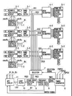
Fig. 3 shows the synchronization acquiring circuit for establishing a
synchronization by receiving a carrier with which the digital signal is
transmitted by the above-described hierarchical transmission method.
As shown in Fig. 3, the synchronization acquiring circuit has numerically
controlled oscillators 1-1 to 1-3, complex calculation circuits 2-1 to 2-3,
band limit filters 3-1 to 3-3, binary phase shift keying (BPSK) demappers
4-1 to 4-3, frame synchronization pattern detection circuits 5-1 to 5-3, a
timing generator 6, a selector 7, a phase error detection circuit 8, a
frequency error calculation circuit 9, a loop filter 10, and an automatic
frequency control (AFC) circuit 11.
The numerically controlled oscillators 1-1 to 1-3 generate sine
wave data sin B, to sin 6 3 and cosine wave data cos 8, to cos 6 3,
respectively. The numerically controlled oscillators 1-1 to 1-3 generate
digital signals representative of the amplitudes of the sine wave data or
cosine wave data corresponding to the phase signals 6, to B 3 received
from the AFC circuit 11, and send them to the complex calculation circuits
CA 02391336 2002-01-25
- 21 -
2-1 to 2-3.
The complex calculation circuits 2-1 to 2-3 are each made of an
inverter, a multiplier and the like, and perform calculations for removing
the phase error and frequency error of the quantized baseband signal.
More specifically, each of the complex calculation circuits 2-1 to
2-3 receives the in-phase component I and quadrature component Q of
the baseband signal containing the phase error and frequency error.
The complex calculation circuits 2-1 to 2-3 also receive the sine wave data
sin 6, to sin 0 3 and cosine wave data cos 6, to cos 0 3 from the
numerically controlled oscillators 1-1 to 1-3. The complex calculation
circuits 2-1 to 2-3 perform an inversion process and the like for the
received sine wave data sin 9, to sin 9 3 and cosine wave data cos 9, to
cos 8 3, and multiply them with the in-phase component I and quadrature
component 0 of the baseband signal to thereby generate I (in-phase)
signals RI1 to R13 and Q (quadrature) signals RQ1 to RQ3.
The complex calculation circuits 2-1 to 2-3 send the generated I
signals RI1 to R13 and Q signals RQ1 to RQ3 to the band limit filters 3-1 to
3-3.
The band limit filters 3-1 to 3-3 are each made of a digital roll-off
filter or the like having the raised cosine characteristics, and limit the
pass
bands of the I signals R11 to RI3 and Q signals RQ1 to RQ3 received from
the complex calculation circuits 2-1 to 2-3 to thereby generate data
waveforms having no inter-code interference. The band limit filters 3-1 to
3-3 send the band-limited I signals D11 to D13 and Q signals DQ1 to DQ3
to the BPSK demappers 4-1 to 4-3.
The band limit filters 3-1 to 3-3 also send the band-limited I signals
D11 to D13 and Q signals DQ1 to DQ3 to the selector 7.
The BPSK demappers 4-1 to 4-3 recover the digital signals from
CA 02391336 2002-01-25
- 22 -
the signal point positions of the baseband signal in the manner opposite
to the BPSK mapping on the transmission side, in order to detect the
frame synchronization pattern 110 of 20 symbols transmitted through
BPSK modulation.
More specifically, upon reception of the I signals DI1 to D13 and Q
signals DQ1 to DQ3 from the band limit filters, the BPSK demappers 4-1
to 4-3 obtain received signal points on the I-Q vector plane on the
reception side such as shown in Figs. 4(a) to 4(h). The BPSK
demappers 4-1 to 4-3 convert the baseband signal into the digital signals
(0 or 1) corresponding to the received signal point positions on the I-Q
vector plane.
As shown in Fig. 5, each of the BPSK demappers 4-1 to 4-3 has
eight BPSK de-mapping circuits 20 to 27.
Each of the BPSK de-mapping circuits 20 to 27 is made of a read
only memory (ROM) and the like, and converts the received signal point
into a digital signal by using one of eight I-Q vector planes having
different phases of BPSK decision criterion border lines BL shown in Figs.
4(a) to 4(h).
More specifically, each of the BPSK de-mapping circuits 20 to 27
specifies a received signal point and converts it into a digital signal, by
using the I-Q vector plane whose BPSK decision criterion border line BL
is rotated by an angle corresponding to 4) = 450 x n (n is an integer
from 0 to 7) from the I-Q vector plane on the transmission side.
It is assumed in the following that the BPSK de-mapping circuit 20
first converts a signal point into a digital signal by using the I-Q vector
plane shown in Fig. 4(a), and sequentially thereafter the BPSK
de-mapping circuits 21 to 27 convert a signal point into a digital signal by
using the I-Q vector planes shown in Figs. 4(b) to 4(h).
CA 02391336 2002-01-25
- 23 -
The BPSK de-mapping circuits 20 to 27 send bit streams BO to B7
of the recovered digital signals to the frame synchronization pattern
detection circuits 5-1 to 5-3.
The frame synchronization pattern detection circuits 5-1 to 5-3
shown in Fig. 3 detect frame synchronization patterns from the digital
signals recovered by the BPSK demappers 4-1 to 4-3. The frame
synchronization pattern detection circuits 5-1 to 5-3 correspond to three
different frequency ranges representative of frequency errors of the
baseband signal. The frame synchronization pattern detection circuits
5-1 to 5-3 receive the bit streams BO to B7 from the BPSK demappers 4-1
to 4-3 and detect a frame synchronization pattern 110.
Specifically, for example, the frame synchronization pattern
detection circuit 5-1 corresponds to a frequency range of 700 kHz of
the frequency error of + 1.3 MHz, the frame synchronization pattern
detection circuit 5-2 corresponds to a frequency range of 700 kHz of
the frequency error of 0 Hz of the frequency error, and the frame
synchronization pattern detection circuit 5-3 corresponds to a frequency
range of 700 kHz of the frequency error of - 1.3 MHz of the frequency
error.
Each of the frame synchronization pattern detection circuits 5-1 to
5-3 has eight synchronization detection circuits 30 to 37 and an OR gate
38 shown in Fig. 6.
The synchronization detection circuits 30 to 37 all have the same
structure having twenty shift registers (delay latches Do to D19), inverters
IN for the logical inversion of predetermined bits, and an AND gate Al, as
shown in Fig. 7.
The AND gate Al outputs a high level voltage when the state
(D19D18D,,...D,Do) of the delay latches Do to D19 takes
CA 02391336 2002-01-25
- 24 -
(1 1 1 01 1 001 1 01 001 01 000). This corresponds to the bit stream of the
frame synchronization pattern 110. When the output of the AND gate Al
take a high potential, it means that one of the synchronization decision
circuits 30 to 37 detected the frame synchronization pattern.
When one of the synchronization detection circuits 30 to 37 detects
the frame synchronization pattern 110, the OR gate 38 notifies this
detection to the timing generator 6.
The timing generator 6 shown in Fig. 3 establishes a frame
synchronization when it is notified from the frame synchronization pattern
detection circuits 5-1 to 5-3 that the frame synchronization pattern 110
was detected.
In this case, the timing generator 6 decides which one of the frame
synchronization pattern detection circuits 5-1 to 5-3 detected the frame
synchronization pattern 110, and sends a selection signal corresponding
to the decided one of the frame synchronization pattern detection circuits
5-1 to 5-3, to the selector 7.
Namely, when the timing generator 6 decides that the frame
synchronization pattern detection circuit 5-1 detected the frame
synchronization pattern 110, it sends the selector 7 a selection signal to
select the I signal DI1 and Q signal DQ1 output from the band limit filter
3-1. When the timing generator 6 decides that the frame synchronization
pattern detection circuit 5-2 detected the frame synchronization pattern
110, it sends the selector 7 a selection signal to select the I signal D12 and
Q signal DQ2 output from the band limit filter 3-2. When the timing
generator 6 decides that the frame synchronization pattern detection
circuit 5-3 detected the frame synchronization pattern 110, it sends the
selector 7 a selection signal to select the I signal D13 and Q signal DQ3
output from the band limit filter 3-2.
CA 02391336 2002-01-25
- 25 -
After the timing generator 6 establishes the frame synchronization,
it derives the TMCC data 111 to identify the frame multiplex configuration,
and sends a TMCC section signal to the frequency error calculation circuit
9 to specify the TMCC section.
The timing generator 6 also sends a switch signal to the AFC
circuit 11 which makes one of the numerically controlled oscillators 1-1 to
1-3 recover a carrier for acquiring the RF channel under the control of the
phase signals 0, to 6 3.
In response to the selection signal from the timing generator 6, the
. selector 7 made of a multiplexer and the like selects a pair of the I
signals
D11 to D13 and Q signals DQ1 to DQ3 output from one of the band limit
filters 3-1 to 3-3. The selector 7 inputs the selected I signal DI and W
signal DQ to the phase error detection circuit 8.
In accordance with the I signal DI and W signal DQ received from
the selector 7, the phase error detection circuit 8 specifies the signal point
position on the I-Q vector plane to obtain a phase error (received signal
phase rotation angle) between the phase of the signal point position and
the absolute phase.
The phase error detection circuit 8 generates a phase error signal
PED corresponding to the obtained phase error, and sends it to the
frequency error calculation circuit 9 and loop filter 10.
The frequency error calculation circuit 9 specifies the TMCC
section from the TMCC section signal received from the timing generator
6, and calculates a difference (error frequency) Of between a desired
frequency and the frequency of the recovered carrier, in accordance with
the phase error in the TMCC section represented by the phase error
signal PED received from the phase error detection circuit 8.
The frequency error calculation circuit 9 notifies the calculated
CA 02391336 2002-01-25
- 26 -
error frequency Af to the AFC circuit 11.
The loop filter is a low pass filter for smoothing the phase error
signal PED received from the phase error detection circuit 8, and supplies
the smoothed phase error signal PED to the AFC circuit 11 as a phase
adjustment signal LOf.
The AFC circuit 11 generates phase signals 9, to 0 corresponding to the error
frequency Af supplied from the frequency
error calculation circuit 9 and the phase adjustment signal LAf supplied
from the loop filter 10.
The AFC circuit 11 supplies the generated phase signals 0, to 6 3
to the numerically controlled oscillators 1-1 to 1-3 to make them generate
the sine wave data sin 9, to sin 9 3 and cosine wave data cos 8, to cos 9 3.
If the baseband signal received at the complex calculation circuit
2-1 contains a frequency error of + 1.3 MHz, the AFC circuit 11 performs
a complex number calculation of the phase signal 6, to set it to such a
value that the phase of the signal point assigned a predetermined signal
(0 or 1) on the transmission side will not rotate.
If the baseband signal received at the complex calculation circuit
2-2 does not contain a frequency error (a frequency error of 0 MHz), the
AFC circuit 11 performs a complex number calculation of the phase signal
6 2 to set it to such a value that the phase of the signal point assigned a
predetermined signal (0 or 1) on the transmission side will not rotate.
If the baseband signal received at the complex calculation circuit
2-3 contains a frequency error of - 1.3 MHz, the AFC circuit 11 performs a
complex number calculation of the phase signal 9 3 to set it to such a
value that the phase of the signal point assigned a predetermined signal
(0 or 1) on the transmission side will not rotate.
The operation of the synchronization acquiring circuit according to
CA 02391336 2002-01-25
_ 27 -
the first embodiment of the invention will be described.
This synchronization acquiring circuit can acquire an RF channel of
BS digital broadcasting in a short time, because it has a plurality of
reception series for detecting a frame synchronization pattern, the
reception series corresponding in number to a plurality of frequency
ranges each being representative of a different frequency error contained
in the baseband signal.
In the synchronization acquiring circuit of the first embodiment of
the invention, the numerically controlled oscillators 1-1 to 1-3, complex
calculation circuits 2-1 to 2-3, band limit filters 3-1 to 3-3, selector 7,
phase error detection circuit 8, frequency error calculation circuit 9, loop
filter 10 and AFC circuit 11 constitute a carrier reproduction loop which
removes the frequency error of the carrier contained in the in-phase
component I and quadrature component Q of the baseband signal input
to the complex calculation circuits 2-1 to 2-3.
More specifically, first the complex calculation circuits 2-1 to 2-3
receive the in-phase component I and quadrature component Q of the
baseband signal which are obtained by detecting the BS-IF signal of the
received radio wave down-converted by an ODU (not shown), by using a
local oscillation signal generated by a local oscillator and having a
frequency fixed to the center frequency of a frequency band assigned to
an RF channel of BS digital broadcasting.
The frequency error generated when ODU down-converts the
received radio wave appears in the BS-IF signal which is an intermediate
signal and also in the baseband signal.
By using the sine wave data sin 0, to sin @ 3 and cosine wave data
cos e, to cos 0 3 received from the numerically controlled oscillators 1-1
to 1-3, the complex calculation circuits 2-1 to 2-3 perform calculations of
CA 02391336 2002-01-25
- 28 -
the formulas 2 to rotate the phase of the baseband signal:
(Formulas 2) Rik = I xcos6k-Qxsin9k
RQk=lxsinek+QxcosBk
where k is an integer of 0 to 3.
If the baseband signal received at the complex calculation circuit
2-1 contains a frequency error of + 1.3 MHz, the AFC circuit 11 performs
a complex number calculation of the phase signal , to set it to such a
value that the phase of the signal point assigned a predetermined signal
(0 or 1) on the transmission side will not rotate.
If the baseband signal received at the complex calculation circuit
2-2 does not contain a frequency error (a frequency error of 0 MHz), the
AFC circuit 11 performs a complex number calculation of the phase signal
02 to set it to such a value that the phase of the signal point assigned a
predetermined signal (0 or 1) on the transmission side will not rotate.
If the baseband signal received at the complex calculation circuit
2-3 contains a frequency error of - 1.3 MHz, the AFC circuit 11 performs a
complex number calculation of the phase signal 0 3 to set it to such a
value that the phase of the signal point assigned a predetermined signal
(0 or 1) on the transmission side will not rotate on the reception side.
Namely, the AFC circuit 11 sets the phase signal 0, to such a
value that the frame synchronization pattern 110 can be detected by
receiving the baseband signal which is contained in the intermediate
frequency signal (BS-IF signal) in a predetermined frequency range
higher than the oscillation frequency of a local oscillation signal
generated by a local oscillator (not shown) and used for
quasi-synchronization detection.
The AFC circuit 11 sets the phase signal 6 2 to such a value that the
frame synchronization pattern 110 can be detected by receiving the
CA 02391336 2002-01-25
- 29 -
baseband signal which is contained in the intermediate frequency signal
(BS-IF signal) in a predetermined frequency range including the same
frequency as the oscillation frequency of a local oscillator (not shown).
The AFC circuit 11 sets the phase signall 9 3 to such a value that
the frame synchronization pattern 110 can be detected by receiving the
baseband signal which is contained in the intermediate frequency signal
(BS-IF signal) in a predetermined frequency range lower than the
oscillation frequency of a local oscillator (not shown).
Upon reception of the phase signals 91 to e 3 from the AFC
circuit 11, the numerically controlled oscillators 1-1 to 1-3 generate the
sine wave data sin B, to sin 6 3 and cosine wave data cos 9, to cos 8 3
and supply them to the complex calculation circuits 2-1 to 2-3.
The complex calculation circuits 2-1 to 2-3 input the obtained I
signals RI1 to R13 and Q signals RQ1 to RQ3 to the band limit filters 3-1 to
3-3 to limit the bands thereof and obtain the I signals D11 to D13 and Q
signals DQ1 to DQ3.
In this manner, the complex calculation circuits 2-1 to 2-3 can
change the frequency of the baseband signal so that the frame
synchronization pattern 110 can be detected in the range of 2 MHz of
the frequency error contained in the baseband signal. Therefore, if the
frequency error generated when ODU down-converts is in the range of
2 MHz, it is possible to detect the frame synchronization pattern and
acquire the RF channel.
The I signals D11 to D13 and Q signals DQ1 to Dq3 output from the
band limit filters 3-1 to 3-3 are input to the BPSK demappers 4-1 to 4-3
and to the selector 7.
The selector 7 selects a pair of the I signals D11 to D13 and Q
signals DQ1 to DQ3 output from one of the band limit filters 3-1 to 3-3,
CA 02391336 2002-01-25
- 30 -
and sends the. pair to the phase error detection circuit 8.
Whether the selector 7 selects which pair of the I signals DI1 to D13
and Q signals DQ1 to DQ3 is determined by the selection signal supplied
from the timing generator 6.
The operations up to outputting the selection signal from the timing
generator 6 will be described.
When the I signals Di1 to D13 and Q signals DQ1 to DQ3 output
from the band limit filters 3-1 to 3-3 are input to the BPSK demappers 4-1
to 4-3, the BPSK de-mapping circuits 20 to 27 recover the digital signals.
In this case, in order to convert the received signal point into the
digital signal, each of the BPSK de-mapping circuits 20 to 27 specifies the
received signal point on the I-Q vector plane having the BPSK decision
criterion border line BL whose phase is rotated so as to match the I-Q
vector plane rotated by 0 = 450 x n (n is an integer of 0 to 7).
The reason why the signal point is converted into the digital signal
by using the eight I-Q vector planes having the BPSK decision criterion
border lines BL whose phases are rotated, is as follows.
Namely, in the hierarchical transmission method of repetitively
transmitting each frame by using a plurality of time division modulation
methods, the TMCC data 111 representative of the transmission
multiplexing configuration identification data indicating the multiplexing
configuration of modulation methods, is derived at the timing generated
by the frame synchronization pulse after the frame synchronization is
established. By identifying the multiplexing configuration of the
modulation method indicated by the TMCC data 111, the processes for
each modulation method can be executed.
Since the 8PSK demodulation is also performed until the. frame
synchronization is established, the phase of the baseband signal may
CA 02391336 2002-01-25
- 31 -
rotate by d~ = 450 x n (n is an integer of 0 to 7) until the frame
synchronization is demodulated, depending upon the phase of the carrier
recovered by the numerically controlled oscillators 1-1 to 1-3 and AFC
circuit 11.
For example, it is assumed that the bit "0" is assigned to the signal
point position "0" shown in Fig. 2(c) and the bit "1" is assigned to the
signal point position "4".
In this case, the signal points for the bits "0" and "1" specified by
the I signals D11 to D13 and Q signals DQ1 to DQ3 received at the BPSK
demappers 4-1 to 4-3 from the band limit filters 3-1 to 3-3, may appear at
the signal point positions "0" and "4" at 0 = 00 shown in Fig. 2(c) which
is same as those of the transmission side.
However, depending upon the phase of the carrier recovered by
the numerically controlled oscillators 1-1 to 1-3 and AFC circuit 11, the
signal points for the bits "0" and "1" may appear at the signal point
positions "1" and "5" at the phase rotation of 0 = 45 shown in Fig. 2(a).
Alternatively, they may appear at the signal point positions "2" and "6" at
the phase rotation of 0 = 90, or may appear at the signal point positions
"0" and "4" at the phase rotation of d) = 135 .
Since the phase may rotate by = 450 x n (n is an integer of 0 to
7) until the frame synchronization pattern 110 is demodulated, it is
necessary to reliably detect the frame synchronization pattern 110 even if
it is demodulated at each of eight phases.
From this reason, each of the BPSK demappers 4-1 to 4-3 has
eight BPSG de-mapping circuit 20 to 27 and converts the signal point into
a digital signal by using one of the eight I-Q vector planes having the
BPSK decision criterion border lines BL whose phases are rotated.
The bit streams (BO to 137) of the digital signal recovered by the
CA 02391336 2002-01-25
- 32 -
BPSK demappers 4-1 to 4-3 are sent to the frame synchronization pattern
detection circuits 5-1 to 5-3.
When the timing generator 6 is notified from one of the frame
synchronization pattern detection circuits 5-1 to 5-3 that the frame
synchronization pattern 110 was detected, it decides which one of the
frame synchronization pattern detection circuits 5-1 to 5-3 detected the
frame synchronization pattern 110, and sends the select signal
corresponding to the decision result.
Namely, if the timing generator 6 decides that the frame
synchronization pattern detection circuit 5-1 detected the frame
synchronization pattern 110, it sends the selection signal to the selector 7
to select the I signal D11 and Q signal DQ1 output from the band limit filter
3-1. If the timing generator 6 decides that the frame synchronization
pattern detection circuit 5-2 detected the frame synchronization pattern
110, it sends the selection signal to the selector 7 to select the I signal
D12
and Q signal DQ2 output from the band limit filter 3-2. If the timing
generator 6 decides that the frame synchronization pattern detection
circuit 5-3 detected the frame synchronization pattern 110, it sends the
selection signal to the selector 7 to select the I signal D13 and Q signal
DQ3 output from the band limit filter 3-3.
In this manner, the timing generator 6 can send the selection signal
for making the selector 7 decide which pair of the I signals DI1 to D13 and
Q signals DQ1 to DQ3 is selected.
At the same time, the timing generator 6 establishes a frame
synchronization at the timing when the timing generator receives a notice
that the frame synchronization pattern 110 was detected, from one of the
frame synchronization pattern detection circuits 5-1 to 5-3. Then, the
timing generator 6 generates a TMCC section signal for specifying the
CA 02391336 2002-01-25
- 33 -
TMCC section and sends it to the frequency error calculation circuit 9.
At the same time, the timing generator 6 sends a switch signal to
the AFC circuit 11 to make it recover the carrier for acquiring an RF
channel. The switch signal corresponds to the decision result of which
one of the frame synchronization pattern detection circuits 5-1 to 5-3
detected the frame synchronization pattern 110.
Namely, if the timing generator 6 decides that the frame
synchronization pattern detection circuit 5-1 detected the frame
synchronization pattern 110, it sends the switch signal to the AFC circuit
11, the switch signal instructing the AFC circuit 11 to control the
numerically controlled oscillator 1-1 by the phase signal 8, and recover
the carrier. If the timing generator 6 decides that the frame
synchronization pattern detection circuit 5-2 detected the frame
synchronization pattern 110, it sends the switch signal to the AFC circuit
11, the swftch signal instructing the AFC circuit 11 to control the
numerically controlled oscillator 1-2 by the phase signal 9 2 and recover
the carrier. If the timing generator 6 decides that the frame
synchronization pattern detection circuit 5-3 detected the frame
synchronization pattern 110, it sends the switch signal to the AFC circuit
11, the switch signal instructing the AFC circuit 11 to control the
numerically controlled oscillator 1-3 by the phase signal 0 3 and recover
the carrier.
The I signal DI and Q signal DQ selected by the selector 7 are sent
to the phase error detection circuit 8.
In accordance with the I signal DI and Q signal DQ received from
the selector 7, the phase error detection circuit 8 specifies the signal point
position on the I-Q vector plane, and calculates the phase error (reception
point phase rotation angle) between the phase of the signal point position
CA 02391336 2002-01-25
34 -
and the absolute phase.
The phase error detection circuit 8 sends a phase error signal PED
corresponding to the calculated phase error to the frequency error
calculation circuit 9 and loop filter 10.
The frequency error calculation circuit 9 specifies the TMCC
section from the TMCC section signal received from the timing generator
6, and calculates a difference (error frequency) Af between the desired
frequency and the frequency of the recovered carrier from the phase error
in the TMCC section indicated by the phase error signal PED received
from the phase error detection circuit 8.
The frequency error calculation circuit 9 notifies the calculated
error frequency A f to the AFC circuit 11.
The loop filter 10 smoothes the phase error signal PED received
from the phase error detection circuit 8 to obtain a phase adjustment
signal LOf which is sent to the AFC circuit 11.
The AFC circuit 11 adjusts one of the phase signals 9, to 0 3
corresponding to the switch signal received from the timing generator 6,
in accordance with the error frequency 0 F notified from the frequency
error calculation circuit 9 and the phase adjustment signal LOf received
from the loop filter 10, and supplies the adjusted phase signal to a
corresponding one of the numerically controlled oscillators 1-1 to 1-3.
In this manner, the sine wave data sin 8, to sin 6 3 and cosine wave
data cos , to cos 3 for removing the frequency error of the carrier
contained in the in-phase component I and quadrature component Q of
the baseband signal input to the complex calculation circuits 2-1 to 2-3
can be generated and the channel having the desired frequency can be
acquired.
As described above, in the synchronization acquiring circuit
CA 02391336 2002-01-25
- 35 -
according to the first embodiment of the invention, the frame
synchronization pattern 110 contained in the baseband signal can be
detected in correspondence with the three frequency ranges
representative of different frequency errors. Therefore, if the frequency
error generated when ODU down-converts a received radio wave is in a
predetermined range (in a range of 2 MHz), the frame synchronization
pattern can be detected quickly.
It is therefore possible to quickly establish a frame synchronization
and acquire an RF channel in a short time.
(Second Embodiment)
A synchronization acquiring circuit according to the second
embodiment of the invention will be described.
Fig. 8 shows the structure of the synchronization acquiring circuit
according to the second embodiment of the invention.
As shown in Fig. 8, the synchronization acquiring circuit has a
numerically controlled oscillator 50, a complex calculation circuit 51, a
band limit filter 52, a BPSK demapper 53, frame synchronization pattern
detection circuits 54-1 to 54-5, a timing generator 55, a phase error
detection circuit 56, a frequency error calculation circuit 57, a loop filter
58,
and an AFC circuit 59.
The numerically controlled oscillator 50 generates sine wave data
sin 0 and cosine wave data cos 0 respectively. The numerically
controlled oscillator 50 generates a digital signal representative of the
amplitude of the sine wave data or cosine wave data corresponding to the
phase signal 0 received from the AFC circuit 59, and sends it to the
complex calculation circuit 51.
The complex calculation circuit 51 is made of an inverter, a
CA 02391336 2002-01-25
- 36 -
multiplier and the like, and performs calculations for removing the phase
error and frequency error of the quantized baseband signal.
More specifically, the complex calculation circuit 51 receives the
in-phase component I and quadrature component Q of the baseband
signal containing the phase error and frequency error. By using the sine
wave data sin 0 and cosine wave data cos 0 received from the
numerically controlled oscillator 50, the complex calculation circuit 51
performs a calculation for rotating the phase of the baseband signal to
thereby generate an I (in-phase) signal RI and a Q (quadrature) signal
RQ.
The complex calculation circuit 51 sends the generated I signal RI
and Q signal RQ to the band limit filter 52.
The band limit filter 52 is made of a digital roll-off filter or the like
having the raised cosine characteristics, and limits the pass band of the 1
signal RI and Q signal RQ received from the complex calculation circuit
51 to thereby generate a data waveform having no inter-code interference.
The band limit filter 52 sends the band-limited I signal DI and Q signal
DQ of the I signal RI and Q signal RQ received from the complex
calculation circuit 51, to the BPSK demapper 53.
The band limit filter 52 also sends the band-limited I signal DI and
Q signal DQ to the phase error detection circuit 56.
The BPSK demapper 53 recovers the digital signal from the signal
point position of the baseband signal in the manner opposite to the BPSK
mapping on the transmission side, in order to detect the frame
synchronization pattern 110 of 20 symbols transmitted through BPSK
modulation.
The BPSK demapper 53 has eight BPSK de-mapping circuits 20 to
27 similar to the synchronization acquiring circuit of the first embodiment.
CA 02391336 2002-01-25
- 37 -
The BPSK de-mapping circuits 20 to 27 send bit streams BO to B7
of the recovered digital signals to the frame synchronization pattern
detection circuits 54-1 to 54-5.
The frame synchronization pattern detection circuits 54-1 to 54-5
detect frame synchronization patterns from the bit streams B0 to B7
output from the BPSK de-mapping circuits 20 to 27 of the BPSK
demapper 53.
Each of the frame synchronization pattern detection circuits 54-1 to
54-5 detects the frame synchronization pattern 110 in the frequency range
corresponding to the frequency error contained in the baseband signal.
For example, the frame synchronization pattern detection circuit
54-1 detects the frame synchronization pattern 110 if the frequency error
of the baseband signal is in the range from + 2.1 MHz to + 1.4 MHz.
Similarly the frame synchronization pattern detection circuits 54-2,
54-3, 54-4, and 54-5 detect the frame synchronization pattern 110 if the
frequency error is in the ranges from + 1.4 MHz to + 700 kHz, from +
700 kHz to - 700 kHz, from -700 kHz to - 1.4 MHz, and from - 1.4 MHz to -
2.1 MHz.
The frame synchronization pattern detection circuit 54-1 has eight
synchronization detection circuits 40-1 to 47-1 and an OR gate 48-1 as
shown in Fig. 9, in order to detect the frame synchronization pattern 110 if
the baseband signal received at the complex calculation circuit 51 has a
frequency error in the range from + 2.1 MHz to + 1.4 MHz.
In order to detect the frame synchronization pattern 110 correctly
in the case that the frequency error of the baseband signal is in the range
from + 2.1 MHz to + 1.4 MHz, for example, as shown in Figs. 10(a) to
10(e), a BPSK decision criterion border line LN on the I-Q vector plane is
rotated four times along the same phase direction while 20 symbols of the
CA 02391336 2002-01-25
- 38 -
frame synchronization pattern are received.
The signal point positions shown in Figs. 10(a) to 10{e) are
assigned to the bit "1" on the transmission side.
The synchronization detection circuits 40-1 to 47-1 of the frame
synchronization pattern detection circuit 54-1 detect the frame
synchronization pattern 110 by using four of the eight bit streams B0 to
B7 received from the eight BPSK de-mapping circuits 20 to 27 of the
BPSK demapper 53.
Consider for example the case wherein the synchronization
detection circuit 40-1 is used as the circuit for detecting the frame
synchronization pattern 110 from the digital signals converted by using
the I-Q vector plane whose BPSK decision criterion border line LN is
rotated in the order shown in Figs. 10(a) to 10(e).
In this case, as shown in Fig. 11, the synchronization detection
circuit 40-1 has six AND gates A10-1 to A15-1, and delay latches Do to D19
serially connected for respective bit streams.
By using the delay latches Do to Dt9, this synchronization detection
circuit 40-1 delays the bit stream B2 received from the BPSK de-mapping
circuit 22 which demaps by using the I-Q vector plane shown in Fig. 4(c).
The AND gate A10-1 outputs a high level voltage when the state
(D3D2D,Do) of the delay latches Do to D3) is (1000). The AND gate A11-1
outputs a high level voltage. when the state (D19D1eDõD16) of the delay
latches D,s to D19 is (1110).
By using the delay latches Do to D15, the synchronization detection
circuit 40-1 delays the bit stream 64 received from the BPSK de-mapping
circuit 24 which demaps by using the I-Q vector plane shown in Fig. 4(e).
The AND gate A12-1 outputs a high level voltage when the state
(D,SDõD13D12) of the delay latches D,2 to Dt5) is (1100).
CA 02391336 2002-01-25
39 -
By using the delay latches Do to D,,, the synchronization detection
circuit 40-1 delays the bit stream B6 received from the BPSK de-mapping
circuit 26 which demaps by using the I-Q vector plane shown in Fig. 4(g).
The AND gate A13-1 outputs a high level voltage when the state
(DõD,0D9D8) of the delay latches D8 to Dõ) is (1101).
By using the delay latches Do to Dõ the synchronization detection
circuit 40-1 delays the bit stream B0 received from the BPSK de-mapping
circuit 20 which demaps by using the I-Q vector plane shown in Fig. 4(a).
The AND gate A14-1 outputs a high level voltage when the state
(D7D6D5D4) of the delay latches D4 to D7) is (0010).
The AND gate A15-1 outputs a high level voltage when all the AND
gates A10-1 to A14-1 output the high level voltage. Therefore, the
synchronization detection circuit 40-1 notifies the timing generator 55 of a
detection of a frame synchronization pattern 110 via the OR gate 48-1.
Similar to the synchronization detection circuit 40-1, the
synchronization detection circuits 41-1 to 47-1 shown in Fig. 9 detect the
frame synchronization pattern 110 by using four of the bit streams B0 to
B7 received from the eight BPSK de-mapping circuits 20 to 27 of the
BPSK demapper 53.
The synchronization detection circuits 40-1 to 47-1 are structured
so that they can deal with different reception point phase rotation angles
by 45 x n (n is an integer of 0 to 7) at the time when the first bits of the
frame synchronization pattern 110 are received.
The synchronization detection circuits 40-1 to 47-1 may share the
delay latches Do to D1e for delaying each of the bit streams B0 to B7. In
this case, the connection wiring is formed in accordance with the state of
the delay latches Do to D19 for obtaining the logical products.
The frame synchronization pattern detection circuit 54-2 shown in
CA 02391336 2002-01-25
- 40 -
Fig. 8 has eight synchronization detection circuits 40-2 to 47-2 and an OR
gate 48-2 as shown in Fig. 12, in order to detect the frame
synchronization pattern 110 if the baseband signal received at the
complex calculation circuit 51 has a frequency error in the range from +
1.4 MHz to + 700 kHz.
In order to detect the frame synchronization pattern 110 correctly
in the case that the frequency error of the baseband signal is in the range
from + 1.4 MHz to + 700 kHz, for example, as shown in Figs. 13(a) to
13(c), the BPSK decision criterion border line LN on the I-Q vector plane
is rotated twice along the same phase direction while 20 symbols of the
frame synchronization pattern are received.
The signal point positions shown in Figs. 13(a) to 13(c) are
assigned to the bit "1" on the transmission side.
The synchronization detection circuits 40-2 to 47-2 of the frame
synchronization pattern detection circuit 54-2 detect the frame
synchronization pattern 110 by using three of the eight bit streams BO to
B7 received from the eight BPSK de-mapping circuits 20 to 27 of the
BPSK demapper 53.
Consider for example the case wherein the synchronization
detection circuit 40-2 is used as the circuit for detecting the frame
synchronization pattern 110 from the digital signals converted by using
the I-Q vector plane whose BPSK decision criterion border line LN is
rotated in the order shown in Figs. 13(a) to 13(c).
In this case, as shown in Fig. 14, the synchronization detection
circuit 40-2 has four gates A10-2 to A13-2, and delay latches D. to D19
serially connected for respective bit streams.
By using the delay latches Do to D,a, this synchronization detection
circuit 40-2 delays the bit stream B2 received from the BPSK de-mapping
CA 02391336 2002-01-25
- 41 -
circuit 22 which demaps by using the I-Q vector plane shown in Fig. 4(c).
The AND gate A10-2 outputs a high level voltage when the state
(D19D18DõD,sD15D14D13) of the delay latches D13 to D,9) is (1110110).
By using the delay latches Do to D12, the synchronization detection
circuit 40-2 delays the bit stream B4 received from the BPSK de-mapping
circuit 24 which demaps by using the I-Q vector plane shown in Fig. 4(e).
The AND gate A11-2 outputs a high level voltage when the state
(Dt2DõD,oD9DeD7) of the delay latches D7to D12) is (011010).
By using the delay latches Do to D6, the synchronization detection
circuit 40-2 delays the bit stream B6 received from the BPSK de-mapping
circuit 26 which demaps by using the I-Q vector plane shown in Fig. 4(g).
The AND gate A12-2 outputs a high level voltage when the state
(D6D5D4D3D2D,Do) of the delay latches Do to D6) is (0101000).
The AND gate A13-2 outputs a high level voltage when all the AND
gates A10-2 to A12-2 output the high level voltage. Therefore, the
synchronization detection circuit 40-2 notifies the timing generator 55 of a
detection of a frame synchronization pattern 110 via the OR gate 48-2.
Similar to the synchronization detection circuit 40-2, the
synchronization detection circuits 41-2 to 47-2 shown in Fig. 12 detect the
frame synchronization pattern 110 by using three of the bit streams B0 to
B7 received from the eight BPSK de-mapping circuits 20 to 27 of the
BPSK demapper 53.
The synchronization detection circuits 40-2 to 47-2 are structured
so that they can deal with different reception point phase rotation angles
by 45 x n (n is an integer of 0 to 7) at the time when the first bits of the
frame synchronization pattern 110 are received.
The synchronization detection circuits 40-2 to 47-2 may share the
delay latches Do to Dt9 for delaying each of the bit streams BO to B7. In
CA 02391336 2002-01-25
- 42 -
this case, the connection wiring is formed in accordance with the states of
the delay latches Do to D19 for obtaining the logical products.
The frame synchronization pattern detection circuit 54-3 shown in
Fig. 8 detects the frame synchronization pattern 110 if the baseband
signal received at the complex calculation circuit 51 has a frequency error
in the range from + 700 kHz to - 700 kHz, and has the same structure as
that of the frame synchronization pattern detection circuits 5-1 to 5-3 of
the first embodiment.
The frame synchronization pattern detection circuit 54-4 detects
the frame synchronization pattern 110 if the baseband signal received at
the complex calculation circuit 51 has a frequency error in the range from
- 700 kHz to - 1.4 MHz. This frame synchronization pattern detection
circuit 54-4 is structured in order to recover the digital signal by rotating
the BPSK decision criterion border line LN twice in the phase direction
opposite to that of the frame synchronization detection circuit 54-2 while
the symbols of the frame synchronization pattern 13 are received.
The frame synchronization pattern detection circuit 54-5 detects
the frame synchronization pattern 110 if the baseband signal received at
the complex calculation circuit 51 has a frequency error in the range from
- 1.4 MHz to - 2.1 MHz. This frame synchronization pattern detection
circuit 54-5 is structured in order to recover the digital signal by rotating
the BPSK decision criterion border line LN four times in the phase
direction opposite to that of the frame synchronization detection circuit
54-2 while the symbols of the frame synchronization pattern 13 are
received.
The timing generator 55 establishes a frame synchronization when
it is notified from the frame synchronization pattern detection circuits 54-1
to 54-5 that the frame synchronization pattern 110 was detected.
CA 02391336 2002-01-25
- 43 -
After the timing generator 55 establishes the frame synchronization,
it derives the TMCC data 111 to identify the frame multiplex configuration,
and sends a TMCC section signal to the frequency error calculation circuit
57 to specify the TMCC section.
When the timing generator 55 receives a notice of a detection of
the frame synchronization pattern 110 from one of the frame
synchronization pattern detection circuits 54-1 to 54-5, it decides which
one of the frame synchronization pattern detection circuits 54-1 to 54-5
detected the frame synchronization pattern. In accordance with this
decision result, the timing generator 55 notifies the AFC circuit 59 of an
off-set frequency for acquiring an RF channel.
In accordance with the I signal DI and W signal DQ received from
the band limit filter 52, the phase error detection circuit 56 specifies the
signal point position on the I-Q vector plane to obtain a phase error
(received signal phase rotation angle) between the phase of the signal
point position and the absolute phase.
The phase error detection circuit 56 generates a phase error signal
PED corresponding to the obtained phase error, and sends it to the
frequency error calculation circuit 57 and loop filter 58.
The frequency error calculation circuit 57 specifies the TMCC
section from the TMCC section signal received from the timing generator
55, and calculates a difference (error frequency) Af between a desired
frequency and the frequency of the recovered carrier, in accordance with
the phase error in the TMCC section represented by the phase error
signal PED received from the phase error detection circuit 56.
The frequency error calculation circuit 57 notifies the calculated
error frequency Af to the AFC circuit 59.
The loop filter 58 is a low pass filter for smoothing the phase error
CA 02391336 2002-01-25
- 44 -
signal PED received from the phase error detection circuit 56, and
supplies the smoothed phase error signal PED to the AFC circuit 59 as a
phase adjustment signal LA f.
The AFC circuit 59 is used for generating a.phase signal 9
corresponding to the error frequency Of supplied from the frequency
error calculation circuit 57 and the phase adjustment signal LAf supplied
from the loop filter 58, so as to recover the carrier.
The AFC circuit 59 controls the numerically controlled oscillator 50
by the phase signal corresponding to the off-set frequency notified
from the timing generator 55, to thereby make the numerically controlled
oscillator 50 generate the sine wave data sin and cosine wave data cos
which allow the frame synchronization pattern detection circuit 54-3 to
detect the frame synchronization patten 110.
Next, the operation of the synchronization acquiring circuit
according to the second embodiment of the invention will be described.
In the synchronization acquiring circuit of the second embodiment
of the invention, the numerically controlled oscillator 50, complex
calculation circuit 51, band limit filter 52, phase error detection circuit
56,
frequency error calculation circuit 57, loop filter 58 and AFC circuit 59
constitute a carrier reproduction loop which removes the frequency error
of the carrier contained in the in-phase component I and quadrature
component Q of the baseband signal input to the complex calculation
circuit 51.
The numerically controlled oscillator 50, complex calculation circuit
51 and band limit filter 52 operate in the manner similar to the numerically
controlled oscillators 1-1 to 1-3, complex calculation circuits 2-1 to 2-3
and band limit filters 3-1 to 3-3 of the synchronization acquiring circuit of
the first embodiment.
CA 02391336 2002-01-25
- 45 -
If the baseband signal received at the complex calculation circuit
51 contains no frequency error (frequency error of 0 Hz), the AFC circuit
59 performs a complex number calculation of the phase signal to set it
to such a value that the phase of the signal point assigned a
predetermined signal (0 or 1) on the transmission side will not rotate on
the reception side.
The I signal DI and Q signal DO output from the band limit filter 52
are input to the BPSK demapper 53 and phase error detection circuit 56.
The BPSK de-mapping circuits 20 to 27 of the BPSK demapper 53
recover digital signals and send them to the frame synchronization
pattern detection circuits 54-1 to 54-5.
The frame synchronization pattern detection circuits 54-1 to 54-5
detect the frame synchronization pattern 110 in the different ranges of a
frequency error of the baseband signal.
Namely, the frame synchronization detection circuit 54-1 detects
the frame synchronization pattern 110 if the frequency error of the
baseband received at the complex calculation circuit 51 is in the range
from + 2.1 MHz to + 1.4 MHz.
Similarly, the frame synchronization detection circuits 54-2 to 54-5
detect the frame synchronization pattern 110, respectively in the
frequency error ranges from + 1.4 MHz to + 700 kHz, from + 700 kHz
to - 700 kHz, from - 700 kHz to - 1.4 MHz, and from - 1.4 MHz to - 2.1
MHz.
The frame synchronization pattern detection circuit 54-3 can detect
the frame synchronization pattern 110, if the center frequency in the
frequency band assigned to an RF channel is down-converted by ODU
(not shown) so as to correspond to the frequency of the intermediate
frequency signal (BS-IF signal) in the predetermined frequency range
CA 02391336 2002-01-25
- 46 -
including the oscillation frequency of the local oscillator (not shown).
The frame synchronization pattern detection circuit 54-2 can detect
the frame synchronization pattern 110, if the center frequency in the
frequency band assigned to an RF channel is down-converted by ODU
(not shown) so as to correspond to the frequency of the intermediate
frequency signal (BS-IF signal) in the predetermined frequency range
higher than the frequency range in which the frame synchronization
pattern detection circuit 54-3 can detect the frame synchronization pattern
110.
The frame synchronization pattern detection circuit 54-1 can detect
the frame synchronization pattern 110, if the center frequency in the
frequency band assigned to an RF channel is down-converted by ODU
(not shown) so as to correspond to the frequency of the intermediate
frequency signal (BS-IF signal) in the predetermined frequency range
higher than the frequency range in which the frame synchronization
pattern detection circuit 54-2 can detect the frame synchronization pattern
110.
The frame synchronization pattern detection circuit 54-4 can detect
the frame synchronization pattern 110, if the center frequency in the
frequency band assigned to an RF channel is down-converted by ODU
(not shown) so as to correspond to the frequency of the intermediate
frequency signal (BS-IF signal) in the predetermined frequency range
lower than the frequency range in which the frame synchronization
pattern detection circuit 54-3 can detect the frame synchronization pattern
110.
The frame synchronization pattern detection circuit 54-5 can detect
the frame synchronization pattern 110, if the center frequency in the
frequency band assigned to an RF channel is down-converted by ODU
CA 02391336 2002-01-25
- 47 -
(not shown) so as to correspond to the frequency of the intermediate
frequency signal (BS-IF signal) in the predetermined frequency range
lower than the frequency range in which the frame synchronization
pattern detection circuit 54-4 can detect the frame synchronization pattern
110.
When the frame synchronization detection circuits 54-1 to 54-5
detect the frame synchronization pattern 110, it notifies this effect to the
timing generator 55.
When the timing generator 55 is notified from one of the frame
synchronization pattern detection circuits 54-1 to 54-5 that the frame
synchronization pattern 110 was detected, in response to this notice, the
timing generator 55 establishes the frame synchronization, generates a
TMCC section signal for specifying the TMCC section, and sends it to the
frequency error calculation circuit 57.
In this case, the timing generator 55 decides which one of the
frame synchronization pattern detection circuits 54-1 to 54-5 detected the
frame synchronization pattern 110, and in accordance with this decision
result, the timing generator 55 notifies the AFC circuit 59 of the off-set
frequency for acquiring the RF channel.
More specifically, if the timing generator 55 decides that the frame
synchronization pattern detection circuit 54-1 detected the frame
synchronization pattern 110, the timing generator 55 notifies the AFC
circuit 59 of the off-set frequency of + 1.75 MHz.
If the timing generator 55 decides that the frame synchronization
pattern detection circuit 54-2 detected the frame synchronization pattern
110, the timing generator 55 notifies the AFC circuit 59 of the off-set
frequency of + 1.05 MHz.
If the timing generator 55 decides that the frame synchronization
CA 02391336 2002-01-25
- 48 -
pattern detection circuit 54-3 detected the frame synchronization pattern
110, the timing generator 55 notifies the AFC circuit 59 of the off-set
frequency of 0 MHz.
If the timing generator 55 decides that the frame synchronization
pattern detection circuit 54-4 detected the frame synchronization pattern
110, the timing generator 55 notifies the AFC circuit 59 of the off-set
frequency of - 1.05 MHz.
If the timing generator 55 decides that the frame synchronization
pattern detection circuit 54-5 detected the frame synchronization pattern
110, the timing generator 55 notifies the AFC circuit 59 of the off-set
frequency of - 1.75 MHz.
The AFC circuit 59 controls the numerically controlled oscillator 50
by the phase signal corresponding to the off-set frequency notified
from the timing generator 55 to generate the sine wave data sin and
cosine data cos
By using the sine wave data sin and cosine data cos defined
by the phase signal corresponding to the off-set frequency, the
complex calculation circuit 51 removes the frequency error contained in
the in-phase component I and quadrature component Q of the baseband
signal.
In this manner, if the frequency error of an RF channel to be
acquired is outside the range of 700 kHz, the frequency error is inside
the range of 35 kHz.
Therefore, when one of the frame synchronization pattern detection
circuits 54-1 to 54-5 detects the frame synchronization pattern 110, the
complex calculation circuit 51 changes the frequency of the baseband
signal so that the frame synchronization pattern detection circuit 54-3 can
detect the frame synchronization pattern.
CA 02391336 2002-01-25
- 49 -
Since the band to be covered by the frame synchronization pattern
detection circuit 54-3 is as broad as 1.4 4MHz, the RF channel can be
stably acquired.
Thereafter, in accordance with the I signal DI and Q signal DQ
received from the band limit filter 52, the phase error detection circuit 56
specifies the signal point position on the I-Q vector plane and obtains the
phase error (received signal phase rotation angle) between the phase of
the signal point position and the absolute phase.
The phase error detection circuit 56 generates the phase error
signal PED corresponding to the obtained phase error, and sends it to the
frequency error calculation circuit 57 and loop filter 58.
The frequency error calculation circuit 57 specifies the TMCC
section from the TMCC section signal received from the timing generator
55, and calculates a difference (error frequency) Af between the desired
frequency and the frequency of the recovered carrier by using the phase
error in the TMCC section indicated by the phase error signal PED
received from the phase error detection circuit 56.
The frequency error calculation circuit 57 notifies the calculated
error frequency Of to the AFC circuit 59.
The loop filter 58 smoothes the phase error signal PED received
from the phase error detection circuit 56 to obtain a phase adjustment
signal L f which is sent to the AFC circuit 59.
The AFC circuit 59 adjusts the phase signal in accordance with
the error frequency A F notified from the frequency error calculation
circuit 57 and the phase adjustment signal L Af received from the loop
filter 58 to control the numerically controlled oscillator 50 and recover the
carrier.
In this manner, the sine wave data sin and cosine wave data cos
CA 02391336 2002-01-25
- 50 -
for removing the frequency error of the carrier contained in the in-phase
component I and quadrature component 0 of the baseband signal input
to the complex calculation circuit 51 can be generated and the channel
having the desired frequency can be acquired.
As described above, in the synchronization acquiring circuit
according to the second embodiment of the invention, the frame
synchronization pattern detection circuits 54-1 to 54-5 are provided for
detecting the frame synchronization pattern 110 in correspondence with
the five frequency ranges representative of different frequency errors
contained in the baseband signal. Therefore, even if the baseband
signal has a large frequency error, the frame synchronization pattern can
be detected instantly. If the frequency error generated when ODU
down-converts is in the predetermined range (in the range of 2 MHz),
the frame synchronization pattern 110 can be detected at once.
When one of the frame synchronization pattern detection circuits
54-1 to 54-5 detects the frame synchronization pattern 110, the off-set
frequency is set so that the frame synchronization pattern detection circuit
54-3 capable of detecting the frame synchronization pattern in the
broadest range of the frequency error, can establish the frame
synchronization.
It is therefore possible to quickly establish a frame synchronization
and acquire an RF channel in a short time and stably.
The present invention is not limited only to receiving BS digital
broadcasting, but is applicable -to any receiver which receives the
baseband signal containing a frequency error and establishes a frame
synchronization.
INDUSTRIAL APPLICABILITY
CA 02391336 2002-01-25
- 51 -
As described so far, according to the present invention, the frame
synchronization pattern is detected in correspondence with the frequency
ranges representative of different frequency errors contained in the
baseband signal, so that the frame synchronization can be established
quickly and an RF channel can be acquired in a short time.
15
25