Note: Descriptions are shown in the official language in which they were submitted.
~ 02391789 2002-06-27
SIN ENHANCER
BACKGItOUNII OF THE INVENTION
Field of the-Invention
The present invention relates to a signal-to-noise (Hereinafter, referred
to "SfN") enhancer, more particuiarly, a signal-to-noise enhancer that is
implemented by using a balun coupler and a rnagnetostatic wave filter.
Description of the Prior Art
Recently; due to miniaturization of a digital broadcasting system, a
satellite broadcasting system; a mobile communication system; a satellite
communication system, a lightweight SIN enhancer that takes little cost is
required. Also, in the characteristic aspect, the S/N enhancer having a low
insertion loss;: a high S/N ratio, a broadband; and low power consumption is
required.
Hereinafter, a conventional S/N enhancer will be explained with
reference to the accompanying drawings.
First, refernng to FIG. 1, the SfN enhancer disclosed in "A Reflection
type of MSW signal to noise enhances in the 404MHz band" of Takao Kuki
and Toshihiro Nomoto, IEEE MTT-S digest voi: 4l, No. 8, pplll-114, 1995
will be explained:
The S/IV enhances comprises a magnetostatic wave filter 10 and a
directional coupler 12. The one end of the magneto static wave filter is
CA 02391789 2005-02-04
'w 50108-2
connected with a circulator or a directional coupler that
the input port and output port are separated. Explaining
the principle thereof, when a RF signal having a small size
thereof is applied to an input port, the signal is converted
into a magnetostatic wave signal at an Yttrium-Iron-Garnet
film. Therefore, the RF input signal is not output to the
output port. Otherwise, when RF input signals equal to and
more than a threshold value are applied to the input port,
almost all the RF signals are reflected to the output port,
without convert into the magnetostatic wave signals.
Accordingly, the S/N enhancer that obtain a high loss when
the signal has a small level and obtain a low loss when the
signal has a large level can be accomplished.
The above-mentioned S/N enhancer has merits which
the structure thereof is simple and the input/output
characteristics is excellent, but has demerits which the
impedance matching as well as a large signal level is
required.
Next, referring to FIG. 2, the S/N enhancer
disclosed in "A signal to Noise'Enhancer using two MSW
filters and its application to Noise reduction in DBS
reception" of Thoshihiro Nomoto and Yoshihiro Matsushita,
IEEE Trans MTT vol. 41, No. 8, pp1316-1322, 1993.8 will be
explained.
The conventional S/N enhancer shown in FIG. 2
comprises magnetostatic wave filters 12~ and 126, a phase
shifter 136, an attenuator 134, and directional couplers 122
and 138. In principle, a first path signal and second path
signal having different level are input to the directional
coupler 122 and are distributed therein. Thereby, these two
2
CA 02391789 2005-02-04
50108-2
signals supplied to the magnetostatic wave filters 124 and
126, respectively. L~h.ere, while the first
2a
CA 02391789 2002-06-27
signal has a high level, the second sigrLal has a low level. That is, the
first
signal includes a noise signal and a desired signal; wherein the noise signal
passes through the rnagnetostatic wave filter 124, without being amplitude
limited, but the desired signal is -amplitude limited: In addition, the-second
signal: has a noise signal and a desired signal which have both level lower
than
that of a saturation threshold powex, thereby the noise level signal and the:
desired signal pass through the magnetostatic filter 126; without being:
amplitude limited.
Next, the directional coupler 138 synthesizes two path signals having
the same amplitude and the opposite phase thereof with respect to the signal
less than the threshold value. At the result; the noise signals are cancelled
and the desired signal of the second signal becomes a main power level signal.
At this time, the level of the threshold power is in the range from
l2dBm (PH) to -l9dBm (PL), forming somewhat of a band. In addition, the
attenuator 134 functions as,a trimmer for compensating the power loss due to
the phase shifter 136.
In the above-mentioned manner, there are merits which the input/output
characteristics thereof is excellent and it is advantageous in the insertion
loss,
but there are derrmerits which it is can be not used at the low power.
SI7MM~RY: OF THE INVENTION
Thus, the object of the present invention is to solve the problems of
prior art and provide a S/N enhancer having a low insertion loss; a high S!N
ratio, broadband.
CA 02391789 2005-02-04
'° 50108-2
In addition, another object of the present
invention is to provide a small-sized S/N enhancer that can
be easily matched with an external circuit in impedance and
can be applicable to the system using the low power or the
high power.
According to the one embodiment of the present
invention, S/N ,enhancer comprising a balun coupler for
dividing an input signal into first and second signals
having the same power, the second signal having the phase
difference of 180 degree with respect to the first signal; a
saturation magnetostatic wave filter for receiving the first
signal output from the balun coupler, converting that into a
first magnetostatic wave signal, and converting the firs
magnetostatic wave signal into a signal having a shape of
the first signal, wherein a power of the first magnetostatic
wave signal is saturated if the first signal has a power of
equal to or more than that of a noise signal; a linear
magnetostatic wave filter for receiving the second signal
from the balun coupler, converting that into a second
magnetostatic wave signal, and converting the second
magnetostatic wave signal into a signal having a shape of
the second signal, wherein the received second signal is
converted into the second magnetostatic wave signal having
an energy linear to a power of the input signal; and a power
synthesizer for synthesizing respective signals output from
the saturation magnetostatic wave filter and the linear
magnetostatic wave filter.
According to another embodiment of the present
invention, a S/N enhancer comprising a balun coupler for
dividing an input signal into a first and second signals
4
CA 02391789 2005-02-04
~~ 50108-2
having the same power, the second signal having the phase
difference of 180 degree with respect to the first signal; a
saturation magnetostatic wave filter for receiving the first
'signal output from the balun coupler, converting that into a
magnetostatic wave signal, and converting the magnetostatic
wave signal into a signal having a shape of the first
signal, wherein a power of the magnetostatic wave signal is
saturated if the first signal has a power of equal to or
more than that of a noise signal; a delay line having the
linearity to transmit the second signal output from the
balun coupler; and a power synthesizer for synthesizing
respective signals output from the saturation magnetostatic
wave filter and the delay line.
BRIEF DESCRIPTION OF THE ATTAC~3ED DRAt~IINGS
The above and other objects, effects, features and
advantages of the present invention will become more
apparent by describing in detail the preferred embodiment of
the present invention with reference to the attached
drawings in which:
FIG. 1 is a schematic block diagram showing a
conventional S/N enhancer;
FIG. 2 is a schematic block diagram showing
another conventional S/N enhancer;
FIG. 3a is a schematic black diagram showing a S/N
enhancer according to a first embodiment of the present
invention;
FIG. 3b is a schematic block diagram showing a S/N
enhancer according to a second embodiment of the present
invention;
5
CA 02391789 2005-02-04
4
' ' 50108-2
FIG. 4 shows an example of a balun coupler in
FIGS. 3a and 3b;
FIG. 5a shows an example of a magnetostatic wave
filter in FIGS. 3a and 3b;
5a
CA .02391789 2002-06-27
FIG. Sb shows the structure of he magnetostatic wave filter connected
with attenuators; and
FIG. 6 shows a power synthesizer in FIGS. 3a and 3b.
Similar reference characters refer to similar parts in the several views ,
of the drawings.
DESCRIPTION OF Tl<IE PREPERRED EMBODIMENT
The embodiments of the present invention wily be explained with:
reference to the accompanyirig.drawings.
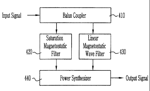
FIG. 3a is a schematic block diagram showing a S/N enhances
according to a first embodiment of the present invention. The SIN enhances
comprises a balun coupler 410, a saturation magnetosatie filter 420, a linear
magnetostatic filter 430, and a power synthesizer 440:
The balun coupler 410 is the balance-to-unbalance: transformer for
receiving one input signal and outputting two output signals Having a phase
difference there between. Each of the two output ignals is output as a
balance signal or an unbalance signal -by dividing into the power of the input
signal at need: The balun coupler employed in the present invention is not
limited to the specific embodiment if it can accomplish the above-mentioned
function. For example, a merchant balun coupler using a micro-strip line has
a broadband width and is implemented by a coaxial line shape or a plane shape.
Hereinafter, the balun coupler 410 will be explained with reference to FIG. 4.
In FIG. 4, an example of the balun coupler 410 is shown. The balun
coupler 410 has an input port A and two output ports B and C, wherein the
6
CA 02391789 2002-06-27
two output signals thereof have a ame power level and a phase difference of
180 degree. In addition; the balun coupler 41p further includes a Z1
transmission line' 412, a Z2 transiriission line 413; and a Z3 ransmission
line ,
414. Also, the Z 1 transmission line 412, the Z2 transmission line 413; the Z3
transmission line 414 have ~; /~, ~: 14, the electrical length of the ~. /4,
and a
characteristic impedance, respectively: Where, ~, means the wavelength of
the propagated signal.
The input signal is input o the input port A of the Z l transmission line
412 and the output signal is output at the output port B to be directed to the
saturation magnetostatic wave filter 420 or the linear znagnetostatic wave
filter
430. The input port B of the Z2 transmission port 413 is grounded, and the
output port thereof is connected to ahe saturation magnetostatic wave: filter
420
or the linear magnetostatic wave filter 430 which is not connected with the
output port B of the Z 1 transmission . line 412; so as to transmit the output
signal: Also; the input port and the output port of the Z3 transmission line
:414 are grounded to induce the coupling.
The trainsmission lines may be composed of; for example, a silver alloy;
a copper, tungsten, or aluminum, may be formed by trimming at least a coil; or
may be formed. by trimming at least a capacitor. Also, the transmission lines
are micro-strip type lines or strip-lute type lines.
The magentostatic wave fibers 420, 430 convert the input signal. such
as a microwave signal to a - magnetostatic wave signal, convert the
magnetostatia wave signal into the signal having the shape of the input signal
again, and output that.
CA 02391789 2002-06-27
The magnetostatic wave filters 420, 430 receive signal output from the
balun coupler 410, respectively, The other words, the balance and unbalance
signals are applied as he input signals of the saturation rnagnetostatie wave
filter 420 and the linear magmetostatic wave filter 430; respectively. The
saturation magnetostatic wave filter 420 saturates the energy of the converted
magnetostatic wave signal such that he input/output characteristics thereof
becomes non-linear, in case where the :power level of the input signal is not
less than a certain threshold value Ptm.- Otherwise; the linear magnetostatic
wave filter 430 converts the input signal into the rnagnetostatic wave signal;
having the energy proportional to the power-level of the input signal, though
the signal passing through the saturation magnetostatic wave filter 420 is
saturated and converted to the magnetostatic wave signal. For example; the
linear magnetostatic wave filter 430 is composed so as to have the saturation
threshold value P~;2 larger than the saturation threshold value P~,1 of the
saturation magnetostatic wave filter 42:0. Therefore; the range of the power
level of the input signal passing ' through the saturation magnetostatic wave
filter 420 can be adjusted the range from the values P~,1 to the values Ptha
such
that the level of the input signal passing hrough the linear magnetostatic
filter
430 can be not saturated. Hereinafter; the principle for: embodying the SIN
enhances according to the present invention using the saturation phenomenon
for converting the electromagnetic wave signal into the magnetostatic wave
signal will be explained. In addition, each of the magnetostatic wave filters
420, 430 converts the converted magnetostatic wave signal into the microwave
signal and outputs that.
CA 02391789 2002-06-27
Hereinafter, the example of the r~aagnetostatic wave filter will be
explained in detail with reference to FIG. Sa. For example,, an Yttrium-Iron-
Garnet film 51~ is grown on a Gadoliurn-Galium-Garnet (GGG) substrate 517,
a strip line 513 is formed on the dielectric substrate 517; and the both sides
of
the dielectric substrate 517 are formed with a magnetostatic wave absorber:
518. When the input microwave signal is input at an input port 511 to be
progressed to an output port SIZ; the input microwave signal is converted into
the magnetostatic vcrave signal ,haring tl~e level proportional to the level
of: the
input power while paSSing through :the: YIG film- 515. Thereafter, the
magnetostatic wave signal is oppositely converted into the microwave signal:
When the microwave signal is converted into the magnetostatic wave signah
the rnagnetostatic wave filter: maintains the linearity thereof until the
power
level of the microwave signal becomes the threshold value P~" but has the
input/output characteristics having the saturation characteristics :when the
power level of the microwave becomes larger than the threshold value Pth.
Generally, the level of the threshold value Pth can be adjusted by varying the
characteristics of the YIG film, the shape of the strip line; the magnetic
field
strength: Accordingly, the saturation magnetostat~c wave filter 42~ and the
linear magnetostatic wave filter 43a can be applied to the present embodiment
by manufacturing each of the ri~agnetostatic filters 420 and 430 such that the
level of the threshold value _ P~ of the linear magnetostatic wave filter 430
becomes larger than that Pthl of the saturation rnagnetostatic wave filter
420.
However, above-mentioned implementation of the saturation magnetostatic
wave filter 420 and the linear magnetostatic wave filter 430 was explained as
CA 02391789 2002-06-27
an example.
Qn the other hand, the saturation magnetosatic filter 420 and the linear'
magnetostatic filter 430 in FIG. Sa may be connected with the attenuators 425,
426. The structure of the - saturation magnetostatic filter 420 and the linear
magnetostatic filter 430 connected with the attenuators 425 and 426 is shown
in FIG. Sb:
The power synthesizer 440 synthesizes the powers of the signals output
from the mag~etostatic wave filters 420, 430: The kind of such 2:1 power
synthesizer 440 is specially limited, and:: can be implemented, for example,
by
a Wilkinson power divider/synthesizer: The power synthesizer 440 of the'
present embodiment has two input ports and an output port, wherein the phase
difference between the input signals is Z 80 degree the output port cancelled
the signals having opposite phase each other and outputs the remaining
signals:
The power synthesizer 440 synthesizes three powers without varying the phase
difference between the two input signals:
FIG. 6 shows an example of above-mentioned power synthesizer 440:
The power synthesizer 440 has two input ports G and H and an output port I
wherein the two input signals are synthesized to output a synthesized signal.
The power synthesize 440 further includes a Z4 transmission line 442 and a
ZS transmission line 443. also; .the Z4 transmission line 442 and the ZS
transmission line 443 have the electrical length of ~, /4 and the
characteristic
impedance of (~ 2)Z0: Where, ~: means the wavelength of the propagated
signal.
Hereinafter, the operation of the S/N erihancer according to the first
CA 02391789 2002-06-27
embodiment will be described:
First, when an input signal is input to the balun coupler 410; the balun
coupler 410 divides the input signal into two balance and unbalance output
signals which the powers thereof are a half of that of the input signal and
the
-phases difference there between is 180 degree arid outputs them to the
saturation magnetostatic wave filter 420 and the .linear. magnetostatic wave
filter 430. At this time, the corr~spQndence of the saturation magnetostatic
wave filter 420 and the linear magnetostatic wave falter 430 for the: balance
and unbalance output signals maybe changed.
Next, in case where the level of he input signal is less than a certain
value (the threshold value of the saturation magnetostatic wave filter 420),
the
signals having' a power level which can be judged as the noise are input to
the'
saturation magnetostatic wave filter 420 and the linear magnetostatic wave
filter 430; and these two signals are converted into the magnetostatic wave
signals having the similar energy in the saturation magnetostatic wave filter
420 and he linear magnetostatic wave filter 430; and then ~e concerted
magnetostatic wave signals- are oppositely converted into the microwave
signals again, thereby the signals having same size and the phase difference
of
18U degree are output. Thereafter, these two signals output from the
magnetostatic wave filters are synthesized in the power synthesizer 440;
thereby the signal is not output of the output port. The reason is because
these signals have same size and opposite phase to be cancelled each other.
Next; in case where the level of the input signal is not less than the
certain value (the threshold value of the saturation magnetostatic wave filter
CA 02391789 2002-06-27
420); since the signal input to the saturation rnagnetostatic wave filter 420
is
not less than the saturation value, the energy of the converted the
magnetostatic wave signal' is saturated to do not exceed the certain value;
but,
in the linear magnetostatic wave filter 430; the signal is converted to the
magnetostatic :wage signal having the energy proportional to the power of the'
input signal. Accordingly; when these signals are oppositely converted again;
the signals having different :power and the phase difference of 180 degree are
output: Thereafter; the these two signals output from the magnetostatic wave
filters are synthesized in the power synthesizer 440 to output the synthesized
signal, wherein the synthesised signal. has mainly the power of the signal
passing hrough the linear magnetostatic wave filter 430:
By the above-mentioned-manner, the S/N enhances that the loss in the
small signal: (noise) is higher than the loss in the large signal can be
accomplished. By the above-mentioned manner, the S/N enhances that can
be miniaturized, can be matched with an external circuit in impedance, arid
can be applicable to a system using the high power or the low power, because
the phase shifter is not used. Also, since he S/N enhances according to the
first embodiment can be implemented by one chip shape; it is advantageous to
mass production.
Hereinafter, the second embodiment according to the present invention
will be described.
FIG: 3b shows the structure of the S/N enhances accoxding. to the
second embodiment of the present invention: The SfN enhances includes a
balun coupler 410; a satura~on magnetostatic wave filter 420; a delay line
450;
CA 02391789 2002-06-27
and a power synthesizer 440.
While the linear magnetostatic wave filter is employed in the first
embodiment, the delay line 450. is employed in the second embodiment: That
is; v~hiie the linear magnetostatic wave filter in the :first embodiment
converts
the signal into the magnetostatic wave signal having the energy proportional
to
the power of the input signal and :oppositely converts the converted signal
into
the microwave signal again; the delay line 454 in the second embodiment
transmits the input power to the power synthesizer 440; maintaining the'
linearity thereof. Since the principle thereof is- er~ual to that of the'
first
embodiment, the explanation thereof will. be omitted.
The above-mentioned SfN enhancer improves the SJN ratio of the
digital images thereby the images having good quality can be received.
According the present invention, the small-sized S/N enhaneer that can
be readily matched with an external circuit in impedance, used at a low powera
and applied to a broadband system can be provided.
In addition; since the. distinction of the images in the multimedia
communication system such : as a digital television and a camera can be
improved, the S/N ratio of the, digital imaged; thereby the images having good
quality can be feceived:
Although the present: invention has been illustrated and: described with
respect to exemplary embodirnentS thereof, the present invention should not be
understood as limited to the specific embodiment; and it should be-understood
by those skilled in he art that the foregoing and various other changes,
omission and additions mayebe made therein and thereto; without departing
Image