Note: Descriptions are shown in the official language in which they were submitted.
WO 01/37011 CA 02392092 2002-05-17 pCT/US00/26281
WRAPAROUND OPTICAL SWITCH MATRIX
FIELD AND BACKGROUND OF THE INVENTTION
The present invention relates to optical switch matrices and. more
particularly.
to an improved optical switch matrix with wraparound architecture
Figure 1 illustrates the prior art optical switch matrix 10 of which the
present
invention is an improvement. This prior art optical switch matrix also is
described as
prior art in US 4,852,958, to Okuyama et al. Matrix 10 connects four input
to waveguides 18 to four output waveguides 20 via four rows (a, b, c, d) of
switches.
Each row includes a 1 x2 switch 12, two 2x2 switches 14 and a 2x 1 combiner
16.
Each 1x2 switch 12 has a single input port 40 and two output ports: an upper
output
port 22 and a lower output port 24. Each 2x2 switch has two input ports and
two
output ports: an upper input port 26, a lower input port 28, an upper output
port 30
and a lower output port 32. Each 2x 1 combiner has two input ports: an upper
input
port 34 and a lower input port 36; and a single output port 42. Input
waveguides 18
are connected to corresponding input ports 40. Output waveguides 20 are
connected
to corresponding output ports 42. In each row, lower output ports 24 and 32
are
connected by intermediate waveguides 38 to lower input ports 28 and 36 of the
2o immediately succeeding switches 14 or 16; whereas upper output ports 22 and
30 are
connected by intermediate waveguides 38 to upper input ports 26 or 34 of
respective
switches 14 or 16 in the cyclically succeeding row. Cyclical succession means
that
the connection topology is as though the rows were fabricated on the periphery
of a
cylinder, parallel to the axis of the cylinder: row b is the successor of row
a, row c is
the successor of row b, row d is the successor of row c and row a is the
successor of
row d. So, for example, an intermediate waveguide 38 connects upper output
port 22
of switch 12d to upper input port 26 of switch l4aa. In Okuyama et al., rows a
and d
are shown connected by intermediate waveguides 38 that cross other
intermediate
waveguides 38. For illustrational clarity, this wraparound of the connectivity
between
3o rows a and d is represented in Figure 1 by the circled terminations A, B
and C on
CA 02392092 2002-05-17
WO 01/37011 PCT/US00/26281
2
intermediate waveguides 38 that connect output ports 22 and 30 in row d to
input
ports 26 and 34 in row a.
Several implementations of 2x2 switches 14 are known in the prior art,
including, among others, directional coupler switches and Mach-Zehnder
interferometer switches. A 2x2 switch 14 can be in one of two states: a
straight-through state (also called the "bar" state or the "_" state), in
which optical
energy, that enters switch 14 via upper input port 26, exits switch 14 via
upper output
port 30, and in which optical energy, that enters switch 14 via lower input
port 28,
exits switch 14 via lower output port 32; and a crossover state (also called
the ''cross''
1 o state or the "X" state") in which optical energy. that enters switch 14
via upper input
port 26, exits switch 14 via lower output port 32, and in which optical
energy, that
enters switch 14 via lower input port 28, exits switch 14 via upper output
port 30.
Switch 14 is switched from one state to another by the application of a
voltage to an
internal component of switch 14. With no voltage applied, switch 14 is "OFF"
in one
of its two states. With the switching voltage applied, switch 14 is "ON" in
the other
of its two states. Two variants of switch 14 thus are possible. In the first
variant,
switch 14 is in its = state when OFF and in its X state when ON. In the second
variant, switch 14 is in its X state when OFF and in its = state when ON. In
the
context of the present invention, the first variant of switch 14 is preferred.
2x2 switch 14 is turned into a 1x2 switch 12 simply by making one of the
input ports an idle port, i.e., leaving this input port disconnected. For
example, if
lower input port 28 is idle, then upper input port 26 serves as input port 40,
upper
output port 30 serves as upper output port 22 and lower output port 32 serves
as lower
output port 24. In the preferred variant of such a 1 x2 switch 12, when this
switch 12
is OFF, it is in its = state, so that optical energy entering via input port
40 leaves via
upper output port 22; and when this switch 12 is ON, it is in its X state. so
that optical
energy entering via input port 40 leaves via lower output port 24.
Alternatively. if
input port 26 is idle, then lower input port 28 serves as input port 40. In
the preferred
variant of this alternative 1x2 switch 12, when this switch 12 is OFF, it is
in its =
3o state, so that optical energy entering via input port 40 leaves via lower
output port 24,
CA 02392092 2002-05-17
WO 01/3701 I PCT/US00/26281
3
and when this switch 12 is ON, it is in its X state, so that optical energy
entering via
input port 40 leaves via upper output port 22.
2x1 combiners 16 may be either passive or active. 2x2 switch 14 is turned into
a 2x 1 active combiner 16 simply by making one of the output ports an idle
port, i. e. ,
leaving this output port disconnected. For example, if lower output port 32 is
idle,
then upper input port 26 serves as upper input port 34, lower input port 28
serves as
lower input port 36, and upper output port 30 serves as output port 42. In
what
follows, an active 2x 1 combiner usually is referred to as a "2x 1 switch". In
the
preferred variant of such a 2x1 switch 16, when this 2x1 switch 16 is OFF, it
is in its =
1 o state, so that only optical energy entering via upper input port 34 leaves
via output
port 42; and when this 2x1 switch 16 is ON, it is in its X state, so that only
optical
energy entering via lower input port 36 leaves via output port 42.
Alternatively, if
upper output port 30 is idle, then lower output port 32 serves as output port
42. In the
preferred variant of this alternative 2x1 switch 16, when this 2x1 switch 16
is OFF, it
is in its = state, so that only optical energy entering via lower input port
36 leaves via
output port 42, and when this 2x 1 switch 16 is ON, it is in its X state, so
that only
optical energy entering via upper input port 34 leaves via output port 42.
Although
2x1 combiners 16 are most simply implemented as passive combiners, such as
y junction combiners, the preferred 2x1 combiners of the present invention are
active
2x1 combiners, both because passive 2x1 combiners are inherently lossy and for
a
second reason describe below.
By turning appropriate switches 12 and 14 ON and OFF, any input waveguide
18 may be connected to any output waveguide 20. For example, let 1x2 switches
12
be 2x2 switches with idle lower input ports, let 1x2 switches 12 and 2x2
switches 14
be in their = states when OFF and in their X states when ON, and let 2x1
combiners
16 be passive. With all switches 12 and 14 OFF, input waveguide 18a is
connected to
output waveguide 20d, input waveguide 18b is connected to output waveguide
20a,
input waveguide 18c is connected to output waveguide 20b, and input waveguide
18d
is connected to output waveguide 20c. Turning switch 12a ON connects input
3o waveguide 18a to output waveguide 20a. Turning switch l4ba ON connects
input
WO 01/37011 CA 02392092 2002-05-17 pCT/jJS00/26281
4
waveguide 18a to output waveguide 20b. Turning switch l4cb ON connects input
waveguide 18a to output waveguide 20c.
By using active 2x 1 combiners 16, optical switch matrix 10 may be configured
so that no input waveguide 18 is connected to any output waveguide 20 unless a
switch 12, 14 or 16 is turned ON. For example, let 1x2 switches 12 and 2x2
switches
14 be as above, and let 2x 1 combiners 16 be 2x2 switches, with idle upper
output
ports, that are in their = states when OFF and in their X states when ON. Now,
with
all switches 12 and 14 OFF, switch 16d must be turned ON to connect input
waveguide 18a to output waveguide 20d, switch 16a must be turned ON to comlect
1 o input waveguide 18b to output waveguide 20a, switch 16b must be turned ON
to
connect input waveguide 18c to output waveguide 20b, and switch 16c must be
turned
ON to connect input waveguide 18d to output waveguide 20c.
SUMMARY OF THE INVENTION
According to the present invention there is provided an optical switch matrix
including: (a) N input waveguides, N being an integer greater than 2; (b) M
output
waveguides, M being an integer greater than 2; and (c) K rows of switch sets,
where K
is a larger of M and N, including: (i) a first switch set having at least one
input port
and two output ports, (ii) a last switch set having two input ports and at
least one
30 output port, and (iii) L-2 intermediate switch sets, where L is a lesser of
M and N, each
intermediate switch set having two input ports and two output ports; wherein
one of
the at least one input ports of each of N of the first switch sets is
optically coupled to a
respective input waveguide; wherein one of the at least one output ports of
each of M
of the last switch sets is optically coupled to a respective output waveguide;
wherein,
for each row, for each switch set other than the last switch set, a first
output port of the
each switch set is optically coupled via a first respective intermediate
waveguide to a
respective input port of a succeeding switch set, and a second output port is
optically
coupled via a second respective intermediate waveguide to a respective input
port of a
respective switch set of a cyclically succeeding row; and wherein, for each
row other
3o than a last row: for each switch set other than the last switch set, the
first and second
intermediate waveguides avoid each other.
WO 01/37011 CA 02392092 2002-05-17 PCT/US00/26281
According to the present invention there is provided an optical switch matrix
including: (a) N input waveguides, N being an integer greater than 2; (b) N
output
waveguides; and (c) N rows of switch sets, all N rows including: (i) a first
switch set
having one input port and two output ports, the input port of the first switch
set being
optically coupled to a respective input waveguide, (ii) a penultimate switch
set having
two input ports and one output port, the output port of the penultimate switch
set of a
last row being optically coupled to a respective output waveguide, and (iii) N-
2
intermediate switch sets, each intermediate switch set having at least one
input port
and two output ports, the intermediate switch sets and the penultimate switch
set of
1o each of a last N-1 rows each having two input ports, each of a last L of a
first N-1
rows, where L is an integer less than N-l, further including: (iv) a last
switch set
having two input ports and one output port, the output port of the last switch
set being
optically coupled to a respective output waveguide, a first input port of the
last switch
set being optically coupled to the output port of the penultimate switch set
of the each
row; wherein the output ports of the penultimate switch sets of a first N L-1
of the
rows are optically coupled to respective output waveguides; wherein, for each
row, for
each switch set selected from the group consisting of the first switch set of
the each
row and the N-2 intermediate switch sets of the each row, a first output port
of the
each switch set is optically coupled via a first respective intermediate
waveguide to a
2o respective input port of a succeeding switch set; wherein, for each of the
first N-1
rows, for each switch set selected from the group consisting of the first
switch set of
the each row and the N-2 intermediate switch sets of the each row, a second
output
port of the each switch set is optically coupled via a second respective
intermediate
waveguide to a respective input port of a respective switch of a succeeding
row; and
wherein, in the last row, for each of a first L switch sets, a second output
port of the
each switch set is optically coupled to a second input port of a respective
last switch
set.
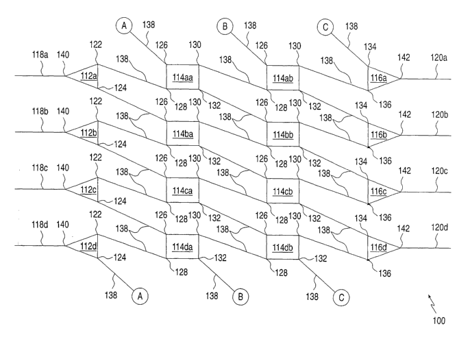
Figure 2 illustrates an optical switch matrix 100 of the present invention.
Matrix 100 connects four input waveguides 118 to four output waveguides 120
via
3o four rows (a, b, c, d) of switch sets 112, 114 and 116. Each switch set
includes one or
more switches such as 1x2 switches, 2x1 combiners or 2x2 switches. The first
(input)
switch set 112 of each row is a 1 x2 switch. In the simplest preferred
embodiment of
WO 01/37011 CA 02392092 2002-05-17 pCT/[JS00/26281
6
matrix 100, each of the intermediate switch sets 114 is a 2x2 switch, but
other
configurations are possible, as described below. The last (output) switch set
116 of
each row is a 2x1 switch. Each 1x2 switch 112 has a single input port 140 and
two
output ports, an upper output port 122 and a lower output port 124. Each
intermediate
switch set 114 has two input ports and two output ports: an upper input port
126, a
lower input port 128, an upper output port 130 and a lower output port 132.
Each 2x 1
switch 116 has two input ports, an upper input port 134 and a lower input port
136,
and a single output port 142. Input waveguides 118 are connected to
corresponding
input ports 140. Output waveguides 120 are connected to corresponding output
ports
o 142. In each row, upper output ports 122 and 130 are connected by
intermediate
waveguides 138 to lower input ports 128 and 136 of the immediately succeeding
switch sets 114 or 116; whereas lower output ports 124 and 132 are connected
by
intermediate waveguides 138 to upper input ports 126 or 134 of respective
switch sets
114 or 116 in the cyclically succeeding row. As in prior art matrix 10, this
connectivity to the cyclically succeeding row wraps around to connect rows a
and d,
as represented in Figure 2 by the circled terminations A, B and C on
intermediate
waveguides 138 that connect output ports 124 and 132 in row d to input ports
126 and
134 in row a.
1x2 switches, such as are used as switch sets 112, also are termed herein
2o "active 1 x2 sputters".
The lack of relatively low angle intra-row crossings of intermediate
waveguides 138 in matrix 100 gives matrix 100 far lower loss than matrix 10.
As
noted above, in Okuyama et al., prior art optical switch matrix 10 is
illustrated as
having intermediate waveguides 38 that connect row d to row a by crossing
other
intermediate waveguides 38. The scope of the present invention includes a
planar
embodiment of matrix 100 with similar wraparound connectivity, but now the
only
intersections of intermediate waveguides 138 in such an embodiment of matrix
100
are intersections that involve intermediate waveguides 138 that connect rows a
and d.
These intersections typically are at high angles and so are characterized by
low loss.
3o All other intermediate waveguides 138 avoid each other. Preferably,
however,
intermediate waveguides 138 that connect rows a and d do not cross other
WO 01/37011 CA 02392092 2002-05-17 pCT/[JS00/26281
7
intermediate waveguides 138 at all, so that all intermediate waveguides 138
avoid
each other. Instead, intermediate waveguides 138 that connect rows a and d
cross
either input waveguides 118 or output waveguides 120, at angles of
approximately 90
degrees. Similarly, in an embodiment of matrix 100 that is fabricated on a
surface
with suitable periodic boundary conditions, such as the side of a cylinder,
all
intermediate waveguides 138 avoid each other without having to cross input
waveguides 118 or output waveguides 120. As yet another alternative, in an
embodiment of matrix 100 that is otherwise fabricated in a single common
plane,
intermediate waveguides 138 that connect rows a and d rise above the plane and
so do
1 o not cross any other waveguides.
As noted above, it is preferable that switch sets 116 be active. If switch
sets
112 are 2x2 switches, with idle lower input ports, that are configured to be
ON in their
= states, passing optical energy from input ports 140 to output ports 122, and
OFF in
their X states, passing optical energy from input ports 140 to output ports
124; if
switch sets 114 are configured to be ON in their = states, passing optical
energy from
input ports 126 to output ports 130 and from input ports 128 to output ports
132, and
OFF in their X states, passing optical energy from input ports 126 to output
ports 132
and from input ports 128 to output ports 130; and if switch sets 116 are 2x2
switches,
with idle lower output ports, that are configured to be ON in their = states,
passing
optical energy from input ports 134 to output ports 142, and OFF in their X
states,
passing optical energy from input ports 136 to output ports 142; then the
algorithm for
deciding which switch group to turn ON to achieve a desired connectivity
between
input waveguides 118 and output waveguides 120 is as simple as in the prior
art.
Starting with all switch sets 112 and 114 OFF, turning ON one of switch sets
116
connects an input waveguide 118 to the output waveguide 120 at the other end
of the
diagonal of matrix 100 into which that input waveguide 118 enters: turning on
switch
set 116d connects input waveguide 118a to output waveguide 120d, turning on
switch
set 116a connects input waveguide 118b to output waveguide 120a, turning on
switch
set 116b connects input waveguide 118c to output waveguide 120b, and turning
on
3o switch set 116c connects input waveguide 118d to output waveguide 120c. To
connect one of input waveguides 118 to a different output waveguide 120, it
suffices
WO 01/37011 CA 02392092 2002-05-17 pCT/[jS00/26281
8
to turn ON only one switch set 112 or 114 with all switch sets 116 OFF. For
example,
to connect input waveguide 118a to output waveguide 120a, switch set 112a is
turned
ON; to connect input waveguide 118a to output waveguide 120b, switch set 114ba
is
turned ON; and to connect input waveguide 118a to output waveguide 120c,
switch
set 114cb is turned ON. Note that in all cases, it suffices to turn ON only
one switch
set 112, 114 or 116 to connect any one input waveguide 118 to any one output
waveguide 120. Optical energy entering matrix 100 from any input waveguide 118
travels along a diagonal of matrix 100 until the switch set 112, 114 or 116
that has
been turned ON diverts the optical energy to the corresponding row of matrix
100.
1 o The same algorithm applies to an alternative embodiment of matrix 100 in
which switch sets 114 are configured to always pass optical energy from input
ports
128 to output ports 130 and to pass optical energy from input ports 126 to
output ports
132 when OFF and from input ports 126 to output ports 130 when ON.
Similarly, in another alternative embodiment of matrix 100 in which switch
sets 112 are configured to pass optical energy from input ports 140 to output
ports 122
when OFF in their = states and to output ports 124 when ON in their X states,
in
which switch sets 114 are configured to always pass optical energy from input
ports
126 to output ports 132 and to pass optical energy from input ports 128 to
output ports
130 when OFF and to output ports 132 when ON, and in which switch sets 116 are
2o configured to pass optical energy from input ports 134 to output ports 142
when OFF
in their = states and from input ports 136 to output ports 142 when ON in
their X
states, the algorithm for deciding which switch group to turn ON to achieve a
desired
connectivity between input waveguides 118 and output waveguides 120 is equally
simple. When all switch sets 112 and 114 are OFF, turning ON one of switch
sets 116
connects a corresponding input waveguide 118 to its default output waveguide
120:
turning on switch set 116a connects input waveguide 118a to output waveguide
120a,
turning on switch set 116b connects input waveguide 118b to output waveguide
120b,
turning on switch set 116c connects input waveguide 118c to output waveguide
120c,
and turning on switch set 116d connects input waveguide 118d to output
waveguide
3o 120d, To connect one of input waveguides 118 to a different output
waveguide 120,
it again suffices to turn ON only one switch set 112 or 114 with all switch
sets 116
CA 02392092 2002-05-17
WO 01/37011 PCT/US00/26281
9
OFF. For example, to connect input waveguide 118a to output waveguide 120b,
switch set 114ab is turned ON; to connect input waveguide 118a to output
waveguide
120c, switch set 114aa is turned ON; and to connect input waveguide 118a to
output
waveguide 120d, switch set 112a is turned ON.
As exemplified in more detail below, a matrix of the present invention can be
configured to connect a certain number of input waveguides 118 to a different
number
of output waveguides 120, essentially by eliminating unneeded switch groups
112,
114 and 116 along diagonals of the matrix, to produce, for N input waveguides
118
and M output waveguides 120, an array having max(M,l~) rows of min(M,N) switch
1 o groups 112, 114 and/or 116 each. Note, however, that both M and N must in
any case
be greater than 2.
In the alternative embodiments of matrix 100, each switch set 114 includes an
active 1x2 switch and a 2x1 combiner. In one such embodiment, one input port
of the
2x 1 combiner serves as, or is optically coupled to, upper input port 126 of
switch set
114; the input port of the 1 x2 switch serves as, or is optically coupled to,
lower input
port 128 of switch set 114; one output port of the 1 x2 switch serves as, or
is optically
coupled to, upper output port 130 of switch set 114; and the output port of
the 2x1
combiner serves as, or is optically coupled to, lower output port 132 of
switch set 114.
In another such embodiment, the input port of the 1x2 switch serves as, or is
optically
coupled to, upper input port 126 of switch set 114; one input port of the 2x 1
combiner
serves as, or is optically coupled to, lower input port 128 of switch set 114;
the output
port of the 2x1 combiner serves as, or is optically coupled to, upper output
port 130 of
switch set 114; and one output port of the 1x2 switch serves as, or is
optically coupled
to, lower output port 132 of switch set 114. In both cases, the remaining
output port
of the 1x2 switch is optically coupled to the remaining input port of the 2x1
combiner.
According to a second aspect of the present invention, an NxN optical switch
matrix such as matrix 100 is enhanced by appending another 2x1 switch set to
L<N-1
of the rows, starting from the next to last row and working upwards. The
former "last
switch sets" (in the case of 4x4 matrix 100, switch sets 116) then are
considered to be
"penultimate" switch sets. The first L switch sets of the last row, instead of
being
WO 01/37011 CA 02392092 2002-05-17 pCT~jJS00/26281
optically coupled to respective switch sets of the first row, are optically
coupled to
respective newly appended "last" switch sets
BRIEF DESCRIPTION OF THE DRAWINGS
5 The invention is herein described, by way of example only, with reference to
the accompanying drawings, wherein:
FIG. 1 illustrates a prior art optical switch matrix;
FIG. 2 illustrates an optical switch matrix of the present invention, for
connecting four input waveguides to four output waveguides;
10 FIG. 3A illustrates an optical switch matrix of the present invention, for
connecting three input waveguides to five output waveguides;
FIG. 3B illustrates an optical switch matrix of the present invention, for
connecting five input waveguides to three output waveguides;
FIG. 4 shows the layout of a 16x16 optical switch matrix of the present
invention, based on 2x2 switches as intermediate switch sets;
FIG. 5 illustrates an intermediate switch set based on an active 1x2 switch
and
a 2x 1 combiner;
Fig 6 illustrates another intermediate switch set based on an active 1x2
switch
and a 2x 1 combiner;
2o FIG. 7 shows a matrix of pairs of 2x2 switches that is topologically
equivalent
to an 8x8 optical switch matrix of the present invention based on the switch
set of
FIG. 8 as input switch sets, the switch set of FIG. ~ with an active 2x 1
combiner as
intermediate switch sets, and the switch set of FIG. 9 as output switch sets;
FIG. 8 illustrates an input switch set based on an active 1 x2 switch and an
active 2x 1 switch;
FIG. 9 illustrates an output switch set based on an active 1x2 switch and an
active 2x 1 switch;
FIG. 10 shows the layout of a 16x 16 optical switch matrix of the present
invention, based on the switch set of FIG. 8 as input switch sets, on the
switch set of
3o FIG. 5 as intermediate switch sets, and on the switch set of Fig. 9 as
output switch sets
WO 01/37011 CA 02392092 2002-05-17 pCT/[JS00/26281
FIG. 11 shows a second 8x8 optical switch matrix of the present invention,
based on first and last switch sets that are single 2x2 switches and on
intermediate
switch sets that are pairs of 2x2 switches;
FIG. 12 shows a third 8x8 optical switch matrix of the present invention,
based
on switch sets that are pairs of 2x2 switches;
FIG. 13 illustrates an optical switch matrix, for connecting four input
waveguides to four output waveguides, according to a second aspect of the
present
invention.
DESCRIPTION OF THE PREFERRED EMBODIMENTS
to The present invention is of an optical switch matrix which can be used to
switch optical signals from input waveguides to output waveguides in a non-
blocking
manner, with relatively low loss and with high extinction ratios.
The principles and operation of an optical switch matrix according to the
present invention may be better understood with reference to the drawings and
the
accompanying description.
Referring again to the drawings, Figure 3A shows a matrix 200 of the present
invention for connecting three input waveguides 218 to five output waveguides
220
via five rows (a, b, c, d, e) of three switch sets 212, 214 and 216 each. Each
1 x2
switch set 212 has a single input port 240 and two output ports, an upper
output port
222 and a lower output port 224. Each intermediate switch set 214 has two
input
ports and two output ports: an upper input port 226, a lower input port 228,
an upper
output port 230 and a lower output port 232. Each 2x1 last switch set 216a,
216b and
216e has two input ports, an upper input port 234 and a lower input port 236,
and a
single output port 242. Each 2x2 last switch set 216c and 216d has two input
ports
and two output ports: an upper input port 244, a lower input port 246, an
upper output
port 248 and a lower output port 250. Each intermediate switch set 214 is in a
X state,
when OFF, that connects upper input port 226 to lower output port 232 and
lower
input port 228 to upper output port 230, and is in a = state, when ON, that
connects
upper input port 226 to upper output port 230 and lower input port 228 to
lower
output port 232. Similarly, each 2x2 last switch set 216c and 216d is in a X
state,
when OFF, that connects upper input port 244 to lower output port 250 and
lower
input port 246 to upper output port 248, and is in a = state, when ON, that
connects
WO 01/37011 CA 02392092 2002-05-17 pCT/IJS00/26281
12
upper input port 244 to upper output port 248 and lower input port 246 to
lower
output port 250. Input waveguides 218 are connected to corresponding input
ports
240 of 1x2 switch sets 212a, 212b and 212c. Preferably, each 1x2 switch set
212 is a
2x2 switch, with an idle lower input port, that is in a X state, when OFF,
that connects
input port 240 to lower output port 224, and is in a = state, when ON, that
connects
input port 240 to upper output port 222. Likewise. it is preferable that each
of last
switch sets 216 of rows a, b and a be a 2x2 switch, with an idle lower output
port, that
is in a X state, when OFF, that connects lower input port 236 to output port
242, and
that is in a = state, when ON, that connects upper input port 234 to output
port 242.
1 o Output waveguides 220a, 220b and 220e are connected to corresponding
output ports
242 of 2x 1 last switch sets 216a, 216b and 216e. Output waveguides 220c and
220d
are connected to corresponding upper output ports 248 of 2x2 last switch sets
216c
and 216d. In each row, upper output ports 222 and 230 are connected by
intermediate
waveguides 238 to lower input ports 228, 236 or 246 of the immediately
succeeding
switch sets 214 or 216; whereas lower output ports 224, 232 and 250 are
connected by
intermediate waveguides 238 to upper input ports 226, 234 or 244 of respective
switch
sets 214 or 216 in the cyclically succeeding row, or, in the case of lower
output ports
224 of 1x2 switch sets 212c and 212d, to input ports 240 of respective switch
sets 212
in the cyclically succeeding row. As in matrix 100, this connectivity to the
cyclically
2o succeeding row wraps around to connect rows a and d, as represented in
Figure 3A by
the circled terminations A and B on intermediate waveguides 238 that connect
output
ports 224 and 232 in row d to input ports 226 and 234 in row a.
The layout of matrix 200 is obtained from the layout of a Sx5 matrix similar
to
matrix 100, with five 1x2 switch sets 112a through 112e, fifteen 2x2
intermediate
switch sets 114aa through 114ec and five 2x1 switch sets 116a through 116e, by
deleting 1x2 switch sets 112d and 112e and all switch sets 114 and 116 that
extend
diagonally and cyclically downward from the deleted 1x2 switch sets, i.e.,
intermediate switch sets 114ea, 114ab, 114bc, 114aa, 114bb and 114cc, and 2x1
switch sets 116c and 116d. Intermediate switch set 114ba becomes intermediate
switch set 214b, intermediate switch set 114ca becomes intermediate switch set
214c,
intermediate switch set 114da becomes 1x2 switch set 212d, intermediate switch
set
WO 01/37011 CA 02392092 2002-05-17 pCT/US00/26281
13
114cb becomes 2x2 last switch set 216c, intermediate switch set 114db becomes
intermediate switch set 214d, intermediate switch set 114eb becomes 1x2 switch
set
212e. intermediate switch set 114ac becomes intermediate switch set 214a,
intermediate switch set 114dc becomes 2x2 last switch set 216d, and
intermediate
switch set 114ec becomes intermediate switch set 214e.
Figure 3B shows a matrix 260 of the present invention for connecting five
input waveguides 268 to three output waveguides 270 via five rows (a, b, c, d
and e)
of three switch sets 262, 264 and 266 each. The layout of matrix 260 is
obtained from
the layout of matrix 200 by rotating matrix 200 by 180 degrees in the plane of
Figure
to 3A and substituting input waveguides 268 for output waveguides 220, output
waveguides 270 for input waveguides 218, first switch sets 262 for last switch
sets
216, last switch sets 266 for first switch sets 212 and intermediate switch
sets 264 for
intermediate switch sets 214. Each 1x2 first switch set 262a, 262d and 262e
has a
single input port 290 and two output ports, an upper output port 272 and a
lower
output port 274. Each 2x2 first switch set 262b and 262c has two input ports
and two
output ports: an upper input port 294, a lower input port 296, an upper output
port 298
and a lower output port 300. Each intermediate switch set 264 has two input
ports and
two output ports: an upper input port 276, a lower input port 278, an upper
output port
280 and a lower output port 282. Each 2x 1 switch set 266 has two input ports,
an
2o upper input port 284 and a lower input port 286, and a single output port
292. Each
intermediate switch set 264 is in an X state, when OFF, that connects upper
input port
276 to lower output port 282 and lower input port 278 to upper output port
280, and is
in a = state, when ON, that connects upper input port 276 to upper output port
280 and
lower input port 278 to lower output port 282. Similarly, each 2x2 first
switch set
262b and 262c is in a X state, when OFF, that connects upper input port 294 to
lower
output port 300 and lower input port 296 to upper output port 298, and is in a
= state,
when ON, that connects upper input port 294 to upper output port 298 and lower
input
port 296 to lower output port 300. Input waveguides 268a, 268d and 268e are
connected to corresponding input ports 290 of 1x2 first switch sets 262a, 262d
and
262e. Input waveguides 268b and 268c are connected to corresponding lower
input
ports 296 of 2x2 first switch sets 262b and 262c. Output waveguides 270 are
WO 01/37011 CA 02392092 2002-05-17 pCT/jJS00/26281
14
connected to corresponding output ports 292 of 2x 1 switch sets 266c, 266d and
266e.
Preferably, each 1 x2 first switch set 262 of rows a, d and a is a 2x2 switch,
with an
idle upper input port, that is in a X state, when OFF, that connects input
port 290 to
upper output port 272, and that is in a = state, when ON, that connects input
port 290
to lower output port 274. Likewise, it is preferable that each 2x1 switch set
266 be a
2x2 switch, with an idle upper output port, that is in an X state, when OFF,
that
connects upper input port 284 to output port 292, and that is an = state, when
ON, that
connects lower input port 286 to output port 292. In each row, upper output
ports
272, 298 and 280 are connected by intermediate waveguides 288 to lower input
ports
I o 278 or 286 of the immediately succeeding switch sets 264 or 266; whereas
lower
output ports 274, 300 and 282 are connected by intermediate waveguides 288 to
upper
input ports 294, 276 and 284 of respective switch sets 262, 264 or 266 in the
cyclically succeeding row; and output ports 292 of 2x1 switch sets 266a and
266b are
connected by intermediate waveguides 288 to upper input ports 284 of
respective 2x 1
switch sets 266 in the cyclically succeeding rows. As in matrices 100 and 200,
this
connectivity to the cyclically succeeding row wraps around to connect rows a
and d,
as represented in Figure 3B by the circled terminations A and B on
intermediate
waveguides 288 that connect output ports 274 and 282 in row d to input ports
276 and
284 in row a.
2o The architecture of matrices 100, 200 and 260 is wide-sense non-blocking,
as
defined by R. A. Spanke, "Architectures for guided-wave optical space
switching
systems", IEEE Communications Vol. 25 No. 5, pp. 42-48, May 1987. The worst
case
accumulated crosstalk in such a matrix that connects N input waveguides 218 to
M
output waveguides 220, due to signal leakage in intermediate switch sets 214
configured as single 2x2 switches, is O-lOloglo(N 1) dB, where 0 is the signal
leakage
in one 2x2 switch. For example, if O is 30 dB and N--16, then the accumulated
crosstalk is 18 dB. Although this is a rather high crosstalk level it is
suitable for
applications in which additional filters, such as wavelength bandpass filters,
are used.
An advantage of this architecture is that it allows the use of relatively long
switches
3o and large numbers of input and output ports on a given substrate.
WO 01/37011 CA 02392092 2002-05-17 PCT/US00/26281
Figure 4 shows a layout of a 16x16 matrix 100, based on 2x2 switches as
intermediate switch sets 114, on a circular face 152 of a 4" cylindrical
silicon wafer
150. In this layout. intermediate waveguides 138, that connect the first row
of the
matrix to the last row of the matrix, cross input waveguides 118. The 1 ~
individual
5 intermediate waveguides 138 that effect this cyclic connectivity from the
last row to
the first row are indicated by respective Roman numerals i through xv where
these
intermediate waveguides 138 depart from the last row and where these
intermediate
waveguides 138 enter the first row.
In some applications, it is important to have high extinction ratios between
t 0 input waveguides 118, 218 or 268 and output ports 120, 220 or 270. In such
a case,
the crosstalk of embodiments of matrices 100, 200 and 260, that are based on
single
2x2 switches as intermediate switch sets 114, 214 and 264, is too high.
Therefore,
intermediate switches sets based on two or more switching elements are used.
Various embodiments of these intermediate switch sets include 1x2 active
switches
15 coupled to either 2x 1 passive combiners or 2x 1 active switches. Although
the scope
of the present invention includes both the embodiments of the intermediate
switch sets
that are based on 2x 1 passive combiners and the embodiments of the
intermediate
switch sets that are based on active 2x1 switches, it is the embodiments with
the
active 2x1 switches that are most preferred because it is the embodiments with
the
2o active 2x1 switches that achieve the required high extinction ratios.
One such intermediate switch set 314 is illustrated in Figure ~. Intermediate
switch set 314 is based on a 1 x2 active switch 312 and a 2x 1 combiner 316. 1
x2
switch 312 has an input port 340, an upper output port 322 and a lower output
port
324. 2x 1 combiner 316 has an upper input port 334, a lower input port 336 and
an
output port 342. Switch set 314 itself has an upper input port 326, a lower
input port
328, an upper output port 330 and a lower output port 332. Internal waveguides
338
connect upper input port 334 of 2x1 combiner 316 to upper input port 326 of
switch
set 314, input port 340 of 1x2 switch 312 to lower input port 328 of switch
set 314,
upper output port 322 of 1 x2 switch 312 to upper output port 330 of switch
set 314,
3o and output port 342 of 2x1 combiner 316 to lower output port 332 of switch
set 314.
Another internal waveguide 338 connects lower output port 324 of 1x2 switch
312 to
CA 02392092 2002-05-17
WO 01/37011 PCT/US00/26281
16
lower input port 336 of 2x1 combiner 316. Although an additional crossing of
waveguides is introduced by having internal waveguide 338, that connects upper
input
port 334 of 2x 1 combiner 316 to upper input port 326 of switch set 314, cross
internal
waveguide 338, that connects upper output port 322 of 1 x2 switch 312 to upper
output
port 330 of switch set 314, these internal waveguides 338 can be configured to
cross
at a relatively large angle, thereby minimizing the associated loss.
1x2 active switch 312 is a 2x2 switch, with an idle lower input port, that is
configured to be in its = state when OFF, passing optical energy from input
port 340
to upper output port 322, and in its X state when ON, passing optical energy
from
1 o input port 340 to lower output port 324. Therefore, switch set 314 passes
optical
energy from lower input port 328 to upper output port 330 when OFF and from
lower
input port 328 to lower output port 332 when ON. If 2x1 combiner 316 is
passive,
then switch set 314 always passes optical energy from upper input port 326 to
lower
output port 332. As described above, to connect one of input waveguides 118,
of a
matrix 100 that uses switch sets 314 as intermediate switch sets 114, and that
uses
switch sets 112 and 116 that are ON in their = states and OFF in their X
states, to one
of output waveguides 120 thereof, it suffices to turn ON only one switch set
112, 114
or 116.
If 2x1 combiner 316 is active, then 2x1 combiner 316 is a 2x2 switch, with an
2o idle lower output port, that is configured to be in its = state, passing
optical energy
from upper input port 334 to output port 342 when OFF, and in its X state,
passing
optical energy from lower input port 336 to output port 342, when ON. In that
case,
with both 1 x2 switch 312 and 2x 1 switch 316 OFF, switch set 314 is in a X
state in
which optical energy entering upper input port 326 leaves via lower output
port 332
and in which optical energy entering lower input port 328 leaves via upper
output port
330. With both 1 x2 switch 312 and 2x 1 switch 316 ON, switch set 314 is in a
modified = state in which optical energy entering upper input port 326 is lost
at the
idle lower output port of 2x1 switch 316 and optical energy entering lower
input port
328 leaves via lower output port 332. If switch set 314 is considered to be ON
when
3o switches 312 and 316 both are ON and if switch set 314 is considered to be
OFF when
switches 312 and 316 both are OFF, then, again, to connect one of input
waveguides
WO 01/37011 CA 02392092 2002-05-17 pCT/jJS00/26281
17
118, of a matrix 100 that uses switch sets 314 as intermediate switch sets
114, and that
uses switch sets 112 and 116 that are ON in their = states and OFF in their X
states, to
one of output waveguides 120 thereof, it suffices to turn ON only one switch
set 112,
114 or 116.
Figure 6 shows another intermediate switch set 414 that is based on a 1x2
active switch 412 and a 2x 1 combiner 416. 1 x2 switch 412 has an input port
440, an
upper output port 422 and a lower output port 424. 2x 1 combiner 416 has an
upper
input port 434, a lower input port 436 and an output port 442. Switch set 414
itself
has an upper input port 426, a lower input port 428, an upper output port 430
and a
lower output port 432. Internal waveguides 438 connect lower input port 436 of
2x 1
combiner 416 to lower input port 428 of switch set 414, input port 440 of 1 x2
switch
412 to upper input port 426 of switch set 414, lower output port 424 of 1 x2
switch
412 to lower output port 432 of switch set 414, and output port 442 of 2x 1
combiner
416 to upper output port 432 of switch set 414. Another internal waveguide 438
connects upper output port 422 of 1 x2 switch 412 to upper input port 434 of
2x 1
combiner 416.
1 x2 switch 412 is a 2x2 switch, with an idle lower input port, that is
configured to be ON in its = state, passing optical energy from input port 440
to upper
output port 422, and OFF in its X state, passing optical energy from input
port 440 to
lower output port 424. Therefore, switch set 414 passes optical energy from
upper
input port 426 to lower output port 432 when OFF and from upper input port 426
to
upper output port 430 when ON. If 2x1 combiner 416 is passive, then switch set
414
always passes optical energy from lower input port 428 to upper output port
430. As
described above, to connect one of input waveguides 118, of a matrix 100 that
uses
switch sets 414 as intermediate switch sets 114 and that uses switch sets 112
that are
OFF in their X states and ON in their = states. to one of output waveguides
120
thereof, it suffices to turn ON only one switch set 112, 114 or 116.
If 2x 1 combiner 416 is active, then 2x 1 combiner 416 is a 2x2 switch with an
idle lower output port, configured to be in its = state, passing optical
energy from
3o upper input port 434 to output port 442 when ON, and in its X state,
passing optical
energy from lower input port 436 to output port 442, when OFF. In that case,
with
WO 01/37011 CA 02392092 2002-05-17 pCT/jJS00/26281
18
both 1 x2 switch 412 and 2x 1 switch 416 OFF, switch set 414 is in a X state
in which
optical energy entering upper input port 426 leaves via lower output port 432
and in
which optical energy entering lower input port 428 leaves via upper output
port 430.
With both 1x2 switch 412 and 2x1 switch 416 ON, switch set 414 is in a
modified =
state in which optical energy entering lower input port 428 is lost at the
idle lower
output port of 2x1 switch 416 and optical energy entering upper input port 426
leaves
via upper output port 430. If switch set 414 is considered to be ON when
switches
412 and 416 both are ON and if switch set 414 is considered to be OFF when
switches
412 and 416 both are OFF, then, again, to connect one of input waveguides 118,
of a
1 o matrix 100 that uses switch sets 414 as intermediate switch sets 114, and
that uses
switch sets 112 and 116 that are OFF in their X states and ON in their =
states, to one
of output waveguides 120 thereof, it suffices to turn ON only one switch set
112, 114
or 116.
In the operational configuration of matrix 100 described above, turning ON
any one switch set 112, 114 or 116 connects input waveguide 118, that feeds
into the
diagonal of matrix 100 on which that switch set 112, 114 or 116 lies, to
output
waveguide 120, that emerges from the row of matrix 100 on which that switch
set
112, 114 or 116 lies. Matrix 100 also can be configured in a reciprocal
operational
configuration, in which turning ON any one switch set 112, 114 or 116 connects
input
2o waveguide 118, that feeds into the row of matrix 100 on which that switch
set 112,
114 or 116 lies, to output waveguide 120, that emerges from the diagonal of
matrix
100 on which that switch set 112, 114 or 116 lies. This is accomplished, for
example,
by using, as switch sets 112, 2x2 switches with idle lower ports that are
configured to
be OFF in their = states, passing optical energy from input ports 140 to
output ports
122, and ON in their X states, passing optical energy from input ports 140 to
output
ports 124; and by using, as switch sets 116, 2x2 switches with idle lower
ports that are
configured to be OFF in their = states, passing optical energy from input
ports 134 to
output ports 142, and ON in their X states, passing optical energy from input
ports 136
to output ports 142. Switch sets 114 are configured as before, to be ON in
their =
3o states, passing optical energy from input ports 126 to output ports 130 and
from input
WO 01/37011 CA 02392092 2002-05-17 pCT~jS00/26281
19
ports 128 to output ports 132, and OFF in their X states, passing optical
energy from
input ports 126 to output ports 132 and from input ports 128 to output ports
130.
Figure 7 shows a matrix 500 of pairs 502, 504 and 506 of 2x2 switches 510,
for connecting eight input waveguides 518 to eight output waveguides 520
according
to the second operational configuration. Matrix 500 is topologically
equivalent to an
8x8 version of matrix 100 that uses intermediate switch sets 314, with active
2x1
combiners 316, as described above, input switch sets 514 of Figure 8 in place
of 1 x2
switches 112, and output switch sets 614 of Figure 9 in place of 2x 1 switches
116.
Input pairs 502 are topologically equivalent to switch sets 514. Intermediate
pairs 504
I o are topologically equivalent to switch sets 314. Output pairs 506 are
topologically
equivalent to switch sets 614.
Input switch set 514 is based on a 1 x2 switch 512 and a 2x 1 switch 516. 1 x2
switch 512 has an input port 540, an upper output port 522 and a lower output
port
524. 2x 1 switch 516 has an idle upper input port 534, a lower input port 536
and an
output port 542. Switch set 514 itself has an input port 526, an upper output
port 530
and a lower output port 532. Internal waveguides 538 connect input port 540 of
1 x2
switch 512 to input port 526 of switch set 514, upper output port 522 of 1x2
switch
512 to upper output port 530 of switch set 514, and output port 542 of 2x 1
switch 516
to lower output port 532 of switch set 514. Another internal waveguide 538
connects
lower output port 524 of 1x2 switch 512 to lower input port 536 of 2x1 switch
516.
1 x2 switch 512 is a 2x2 switch. with an idle lower input port, that is
configured to be in its = state, passing optical energy from input port 540 to
upper
output port 522, when OFF, and in its X state, passing optical energy from
input port
540 to lower output port 524, when ON. 2x 1 switch 516 is a 2x2 switch, with
an idle
lower output port, configured to be in its = state, which would pass optical
energy
from upper input port 534 to output port 542 if upper input port 534 were not
idle.
when OFF, and in its X state, passing optical energy from lower input port 536
to
output port 542, when ON. Switch set 514 is considered OFF when both 1x2
switch
512 and 2x 1 switch 516 are OFF, so that optical energy entering switch set
514 via
input port 526 leaves switch set 514 via upper output port 530. Switch set 514
is
considered ON when both 1 x2 switch 512 and 2x 1 switch 516 are ON, so that
optical
CA 02392092 2002-05-17
WO 01/37011 PCT/US00/26281
energy entering switch set 514 via input port 526 leaves switch set 514 via
lower
output port 532.
Output switch set 614 is based on a 1 x2 switch 612 and a 2x 1 switch 616. 1
x2
switch 612 has an input port 640, an idle upper output port 622 and a lower
output
5 port 624. 2x 1 switch 616 has an upper input port 634. a lower input port
636 and an
output port 642. Switch set 614 itself has an upper input port 26, a lower
input port
628 and an output port 630. Internal waveguides 638 connect input port 640 of
1x2
switch 612 to lower input port 628 of switch set 614, upper input port 634 of
2x 1
switch 616 to upper input port 626 of switch set 614, and output port 642 of
2x 1
1 o switch 616 to output port 630 of switch set 614. Another internal
waveguide 638
connects lower output port 624 of 1 x2 switch 612 to lower input port 636 of
2x 1
switch 616.
1 x2 switch 612 is a 2x2 switch, with an idle lower input port, that is
configured to be in its = state, which would pass optical energy from input
port 640 to
15 upper output port 622 if upper input port 622 were not idle, when OFF, and
in its X
state, passing optical energy from input port 640 to lower output port 624,
when ON.
2x1 switch 616 is a 2x2 switch, with an idle lower output port, that is
configured to be
in its = state, passing optical energy from upper input port 634 to output
port 642,
when OFF, and in its X state, passing optical energy from lower input port 636
to
20 output port 642, when ON. Switch set 614 is considered OFF when both 1x2
switch
612 and 2x 1 switch 616 are OFF, so that optical energy entering switch set
614 via
upper input port 626 leaves switch set 614 via output port 630 and optical
energy
entering switch set 614 via lower input port 628 is lost at idle upper output
port 622 of
1 x2 switch 612. Switch set 614 is considered ON when both 1 x2 switch 612 and
2x 1
switch 616 are ON, so that optical energy entering switch set 614 via upper
input port
626 is lost at the idle lower output port of 2x1 switch 616 and optical energy
entering
switch set 614 via lower input port 628 leaves switch set 614 via output port
630.
In an embodiment of matrix 100 or 200 in which switch sets 314 having active
2x1 switches 316 are used as intermediate switch sets 114 or 214, in which
switch sets
514 are used as input switch sets 112 or 212, and in which switch sets 614 are
used as
output switch sets 116 or 216. any noise added to the signal must traverse two
closed
WO 01/37011 CA 02392092 2002-05-17 pCT/US00/26281
21
switches. Therefore, the worst case accumulated crosstalk, in such a matrix
that
connects N input waveguides to M output waveguides, is 20-lOlog~o(N 1) dB,
where
4 is the signal leakage in one of switches 312 or 316. For example, if O is 30
dB and
N 16, then the accumulated crosstalk is 48 dB. This architecture also has the
advantage of the OFF state of the switches being asymmetric and so relatively
insensitive to production tolerances.
Figure 10 shows a layout of a 16x16 matrix 500, on a circular face 552 of a 4"
cylindrical silicon wafer 550. As in the layout of Figure 4, intermediate
waveguides
548, that connect the first row of the matrix to the last row of the matrix,
cross input
1o waveguides 518; and the 1~ individual intermediate waveguides 548 that
effect this
cyclic connectivity from the last row to the first row are indicated by
respective
Roman numerals i through xv where these intermediate waveguides 548 depart
from
the last row and where these intermediate waveguides 548 enter the first row.
For
illustrational clarity, only some of 2x2 switches 510 are shown in Figure 10.
Figure 11 shows a matrix 700 of switch sets 712, 714 and 716 for connecting
eight input waveguides 718 to eight output waveguides 720. First switch sets
712 are
2x2 switches whose upper input ports are idle and that are configured to be in
their =
states when OFF and in their X states when ON. Similarly, last switch sets 716
are
2x2 switches whose upper output ports are idle and that are configured to be
in their =
2o states when OFF and in their X states when ON. Each intermediate switch set
714
includes two 2x2 switches 702 and 706, connected according to the topology of
switch set 414 of Figure 6. Intermediate switch set 714 is the embodiment of
switch
set 414 with a 2x1 switch 416, with the following modifications: 1x2 switch
412 now
is a 2x2 switch 702 whose upper input port is idle, 2x1 switch 416 now is a
2x2
switch 706 whose upper output port is idle, and switches 702 and 706 are in
their =
states when OFF and in their X states when ON. Topologically, matrix 700 is
equivalent to an 8x8 version of matrix 100. Matrix 700 operates according to
the first
operational configuration of matrix 100: optical energy entering matrix 700
from any
input waveguide 718 travels along a diagonal of matrix 700 until diverted to a
row of
3o matrix 700 by an ON switch set 712, 714 or 716. As before, to route optical
energy
from any one input waveguide 718 to any one output waveguide 720, it suffices
to
WO 01/37011 CA 02392092 2002-05-17 pCT/US00/26281
22
turn ON only one switch set 712, 714 or 716, while leaving all the other
switch sets
off.
Figure 12 shows a matrix 800 of switch sets 802, 804 and 806 for connecting
eight input waveguides 818 to eight output waveguides 820. Each first switch
set 802
includes two 2x2 switches, a 2x2 switch 812 with an idle upper input port and
a 2x2
switch 822 with both an idle lower input port and an idle upper output port.
Each
intermediate switch set 804 includes two 2x2 switches, a 2x2 switch 814 with
an idle
upper input port and a 2x2 switch 824 with an idle upper output port.. Each
last
switch set 806 includes two 2x2 switches, a 2x2 switch 816 with an idle upper
input
3 o port and a 2x2 switch 826 with an idle upper output port. The topology of
matrix 800
is similar to the topology of matrix 700, so that, like matrix 700, matrix 800
is
topologically equivalent to an 8x8 version of matrix 100. The principle
difference
between matrix 700 and matrix 800 is that in matrix 700, each first switch set
712 and
each last switch set 716 includes a single 2x2 switch, whereas in matrix 800,
each first
switch set 802 and each last switch set 806 includes two 2x2 switches. The
lower
input port of switch 812 serves as the input port of switch set 802. The lower
output
port of switch 812 serves as the lower output port of switch set 502. The
lower output
port of switch 822 serves as the upper output port of switch set 502. The
upper output
port of switch 812 is optically coupled to the upper input port of switch 822
by an
2o internal waveguide 832. The lower input port of switch 816 serves as the
upper input
port of switch set 806. The lower input port of switch 826 serves as the lower
input
port of switch set 806. The lower output port of switch 826 serves as the
output port
of switch set 806. The upper output port of switch 816 is optically coupled to
the
upper input port of switch 826 by an internal waveguide 836.
The lower input port of switch 814 serves as the upper input port of switch
set
804. The lower input port of switch 824 serves as the lower input port of
switch set
804. The lower output port of switch 814 serves as the lower output port of
switch set
804. The lower output port of switch 824 serves as the upper output port of
switch set
804. The upper output port of switch 814 is optically coupled to the upper
input port
of switch 824 by an internal waveguide 834.
WO 01/37011 CA 02392092 2002-05-17
PCT/US00/26281
7J
All switches 812, 822, 814, 824, 816 and 826 are configured to be in their =
states when OFF and in their x states when ON. A first switch set 802 is
considered
OFF when both switches 812 and 822 thereof are OFF, and ON when both switches
812 and 822 thereof are ON. An intermediate switch set 804 is considered OFF
when
both switches 814 and 824 thereof are OFF, and on when both switches 814 and
824
thereof are ON. A final switch set 806 is considered OFF when both switches
816 and
826 thereof are OFF, and ON when both switches 816 and 826 thereof are ON.
Optical energy entering matrix 800 via any input waveguide 818 travels along a
diagonal of matrix 800 until diverted by an ON switch set 802, 804 or 806 to a
row of
matrix 100. To route optical energy from any one input waveguide 818 to any
one
output waveguide 820, it suffices to turn ON only one switch set 802, 804 or
806,
while leaving all the other switch sets OFF.
Figure 13 illustrates an alternative optical switch matrix 1100 of the present
invention. Like matrix 100, matrix 1100 connects four input waveguides 1118 to
four
output waveguides 1120 via four rows (a, b, c, d) of switch sets 1112, 1114,
1116 and
1166. Like switch sets 112, the first (input) switch set 1112 of each row is
an active
1 x2 switch. In row a, intermediate switch sets 1114 also are active 1 x2
switches. In
the other rows, intermediate switch sets 1114 are, like switch sets 114,
either single
2x2 switches or combinations of two or more switches, as described above in
the
2o context of matrices 100, 200 and 500. Intermediate switch sets 1114 are
followed in
each row by an active 2x1 switch 1116. In two of the four rows, specifically,
in rows
b and c, active 2x 1 switch 1116 is in turn followed by another active 2x 1
switch 1166.
Because switch sets 1116 may or may not be followed by more switch sets in
their
respective rows, switch sets 1116 are referred to herein as "penultimate"
switch sets,
whereas only switch sets 1166 are referred to as "last" switch sets.
Each 1 x2 switch 1112 has a single input port 1140 and two output ports. an
upper output port 1122 and a lower output port 1124. Each intermediate switch
set
1114 of row a has a single input port 1127; each intermediate switch set 1114
of rows
b, c and d has two input ports: an upper input port 1126 and a lower input
port 1128.
3o Each intermediate switch set 1114 has two output ports: an upper output
port 1130
and a lower output port 1132. Each 2x 1 switch 1116 has two input ports, an
upper
WO 01/37011 CA 02392092 2002-05-17 pCT/US00/26281
24
input port 1134 and a lower input port 1136, and a single output port 1142.
Each 2x 1
switch 1166 has two input ports, an upper input port 1174 and a lower input
port
1176, and a single output port 1182. Input waveguides 1118 are connected to
corresponding output ports 1140. Output waveguides 1120 are connected to
corresponding output ports of the rightmost switch sets in their respective
rows:
output ports 1142 in rows a and d and output ports 1182 in rows b and c. In
row a,
upper output ports 1122 and 1130 are connected by intermediate waveguides 1138
to
input ports of the immediately succeeding switch sets: either input ports 1127
or lower
input port 1136 of switch set 1116a. In the other rows, upper output ports
1122 and
1 o 1130 are connected by intermediate waveguides 1138 to lower input ports
1128 and
1136 of the immediately succeeding switch sets 1114 or 1116. In the first
three rows,
lower output ports 1124 and 1132 are connected by intermediate waveguides 1138
to
upper input ports 1126 or 1134 of respective switch sets 1114 or 1116 of the
succeeding rows. In row d, only lower output port 1132 of intermediate switch
set
15 1114db is connected by an intermediate waveguide 1138 to an upper input
port (1134)
of cyclically succeeding row a. The other two lower output ports are connected
by
intermediate waveguides 1138 to respective upper input ports 1174 of last
switch sets
1166 of rows b and c. Lower input ports 1176 of last switch sets 1166 are
connected
by intermediate waveguides 1138 to output ports 1142 of penultimate switch
sets
2o 1116 of their respective rows.
Let switch sets 1112 be 2x2 switches, with idle upper input ports, that are
configured to be ON in their = states, passing optical energy from input ports
1140 to
output ports 1124, and OFF in their X states, passing optical energy from
input ports
1140 to output ports 1122. Let switch sets 1114aa and 1114ab be 2x2 switches,
with
25 idle upper input ports, that are configured to be ON in their = states,
passing optical
energy from input ports 1127 to output ports 1132, and OFF in their X states,
passing
optical energy from input ports 1127 to output ports 1130. Let the remaining
intermediate switch sets 1114 be configured to be ON in their = states,
passing optical
energy from input ports 1126 to output ports 1130 and from input ports 1128 to
output
3o ports 1132, and OFF in their X states, passing optical energy from input
ports 1126 to
output ports 1132 and from input ports 1128 to output ports 1130. Let switch
sets
WO 01/3701 I CA 02392092 2002-05-17 pCT~jS00/26281
7J
1116 and 1166 be 2x2 switches, with idle upper output ports, that are
configured to be
ON in their = states, passing optical energy from input ports 1136 or 1176 to
output
ports 1142 or 1182, and off in their X states, passing optical energy from
input ports
1134 or 1174 to output ports 1142 or 1182. Then optical energy entering matrix
1100
via any input waveguide travels along a row of matrix 1100 until diverted to a
diagonal of matrix 1100 by an ON switch set 1112, 1114 or 1116. The following
table shows which switch sets must be turned ON to achieve desired
connectivity
between input waveguides 118 and output waveguides 120.
1118a 1118b 1118c 1118d
1120a 1116a 1112b 1114ca 1114db
1120b 1114ab,1166b1116b,1166b 1112c 1114da
1120c 1114aa, 1166c1114bb, 1166c1116c, 1166c1112d
1120d 1112a 1114ba 1114cb 1116d
I o Unlike the switching algorithm for matrix 100, which always requires only
one switch
to be turned ON, the switching algorithm for matrix 1100 sometimes requires
two
switches to be turned on. The advantage of matrix 1100 over matrix 100 is
that,
whereas all the connections in matrix 100 traverse four switch sets, some of
the
connections in matrix 1100 traverse fewer than four switch sets. Specifically,
the
connection from input waveguide 1118d to output waveguide 1120c traverses only
two switch sets (1112d and 1166c), the connection from input waveguide 1118c
to
output waveguide 1120b traverses only three switch sets (1112c, 1114da and
1166b),
and the connection from input waveguide 1118d to output waveguide 1118b
traverses
only three switch sets (1112d, 1114da and 1166b).
2o In general, in an optical switch matrix, such as matrix 1100, for
connecting N
input waveguides to N output waveguides, there are L<N-1 rows with first,
intermediate, penultimate and final switch sets, and N L rows with only first,
intermediate and penultimate switch sets. Specifically, the first N L-1 rows
and the
last row have only first, intermediate and penultimate switch sets, and the
remaining
rows have all four kinds of switch sets. The lower output ports of the first L
switch
sets of the last row are optically coupled to the upper input ports of the
final switch
WO 01/37011 CA 02392092 2002-05-17 pCTnJS00/26281
26
sets, in reverse order: the lower output port of the first switch set of the
last row is
optically coupled to the upper input port of the last switch set of the next-
to-last row.,
the lower output port of the first intermediate switch set of the last row is
optically
coupled to the upper input port of the last switch set of the second-to-last
row, the
lower output port of the second intermediate switch set of the last row is
optically
coupled to the upper input port of the last switch set of the third-to-last
row, etc.
While the invention has been described with respect to a limited number of
embodiments, it will be appreciated that many variations, modifications and
other
applications of the invention may be made.