Note: Descriptions are shown in the official language in which they were submitted.
CA 02392119 2002-06-28
-1-
Title: A BACK REFLECTION INSENSITIVE ELECTRO-
OPTICAL INTERFACE AND A METHOD OF COUPLING THE
SAME TO A WAVEGUIDE
FIELD OF THE INVENTION
This invention relates generally to the field of
telecommunications and more particularly to optical signal-based
telecommunications. Most particularly this invention relates to
electro-optical assemblies for connecting semiconductor laser
optical signal sources to optical signal transmitting waveguides such
as optical fibres and the like.
BACKGROUND OF THE INVENTION
There are a variety of optical signal sources used for creating
carrier signals for optical signal-based telecommunication systems.
One type of signal source is a semiconductor laser that has certain
advantages in being easy to manufacture in large quantities at a
reasonable cost. There are many different types of such
semiconductor laser signal sources including edge emitting
semiconductor lasers, vertical cavity surface emitting lasers and
more recently horizontal cavity surface emitting lasers.
Low-cost signal sources are urgently required to extend the
optical-based networks from the present long haul backbone ring
portions to local nodes closer to the end user, the latter being the
so-called 'metro' portion of the network. While large and expensive
signal sources are justifiable in the long haul backbone portions, the
same cannot be said for all of the internal network nodes in a metro
area. Infilling the network, bringing the optical signals closer and
closer to the end user, is conditional upon being able to provide low
cost high quality signal sources in large volumes to provide the vast
CA 02392119 2002-06-28
-2-
number of required carrier signal sources for the metro portion of
the network. To date there have been efforts to provide such signal
sources, but the prior art signal sources suffer from numerous
disadvantages and thus have not been deployed in a widespread
fashion.
No matter what form the optical signal emitter takes there is
a need to couple the signal light output to an optical waveguide,
such as an optical fibre. Much effort has been devoted to designing
the signal source or emitter to yield an output signal of sufficient
power and signal quality that it can be efficiently and effectively
coupled to the fibre or the like. Thus, the art teaches various
designs of semiconductor which are claimed to produce a Gaussian
shaped far field signal which can be easily and efficiently coupled
to a fibre.
An electro-optical interface can be considered to be a point
in a telecommunications network where the electrical signals are
converted into optical signals in one direction and optical signals are
converted to electrical signals in the other direction. A major
concern in developing an appropriate signal source for the metro
network portion of an optical network is the cost of the signal
source. This is because there is a need for a separate signal
source for each optical channel of the telecommunications band and
separate signal sources at each electro-optical interface in the
network. A low cost design is therefore required if the general
deployment of such optical signal sources is to occur. The cost of
the signal source can be divided into two main components. The
first is the actual capital cost of the optical signal source. The
second is the packaging cost of packaging the signal source
together with whatever other components may be required to couple
the signal source to a waveguide such as a fibre or the like.
CA 02392119 2002-06-28
-3-
Optical feedback is a known phenomenon, which can have
a dramatic effect on the performance of laser signal sources. This
property can be used to improve the optical signal output, through
a so-called external cavity configuration. For example, if the
longitudinal mode selection of the laser is made by other means,
such as a grating reflector, the external feedback may be used for
tuning the laser emission frequency or for a considerable line width
narrowing. An external cavity having controlled external reflection
or feedback may also be useful for reducing the signal chirp. Thus,
prior art designs have made use of controlled feedback to improve
signal characteristics in some cases. Usually such feedback, while
leading to lower chirp and narrower lines, will also result in a lower
bandwidth making the laser more difficult to modulate at high rates.
While controlled optical feedback may be useful as noted
above, uncontrolled optical feedback can have the opposite effect.
Uncontrolled optical feedback, also referred to as back reflection,
can arise from any interface or scattering center in an optical
network. Common sources of detrimental feedback include simple
interfaces or partially reflective surfaces associated with a fibre
pigtail connection in an optical network. Back reflection can travel
along an optical path or waveguide and need not originate in the
immediate environs of the signal source. When back reflected signal
light couples back into the laser cavity, changes in the resonance
condition arise causing often significant changes to the laser output.
A back reflection into a laser cavity can also be considered as
setting up a second cavity having many more modes than the
original. Detrimental effects to signal quality include instabilities in
the output signal power, mode hopping, wavelength shifts,
increased noise and increased spectral line width of up to several
tens of Gigahertz. These instabilities are also referred to as
CA 02392119 2002-06-28
-4-
"coherence collapse" and arise when the back reflection enters into
the laser cavity and detrimentally affects the lasing phenomenon.
To avoid the uncontrolled effects of back reflection, an optical
isolator is required in all but the least demanding of applications. An
optical isolator is defined as an element that allows light to pass in
one direction only and is typically deployed to allow the outgoing
signal light to pass while preventing back reflections from passing
and entering into the cavity thus disturbing the laser stability.
Isolators are normally placed between the signal source and the
optical fiber or waveguide. Typically a lens is placed prior to the
isolator to collimate the tight output from the optical signal source
through the isolator and a second lens is used to couple the light
into the optical fiber or waveguide. The isolator must be placed and
configured in a; way to prevent detrimental back reflections from
entering into the laser cavity, since such back reflections can cause
the unwanted changes to the cavity characteristics and the loss of
signal quality noted above.
The need for an optical isolator as explained has several
undesirable consequences. Firstly, the further the signal source is
away from the end of the fibre with which it is to be optically
coupled, the more difficult and precise the alignments of the
intervening components need to be. The more difficult the
alignment, the more difficult the packaging becomes, thus lowering
the manufacturing yields and increasing the packaging expense.
The complexity of alignment increases nonlinearly with the number
of elements required as the alignment errors in each element are
cumulative for the overall alignment. t.astly of course there is the
actual cost of the additional components, such as the isolator and
any required tensing that is in many cases even more costly than
the signal source.
CA 02392119 2002-06-28
-5-
Figure 1 shows a typical Coarse Wavelength Division
Multiplexed (CWDM) optical signal source 10, in the form of a laser
semiconductor chip coupled to a fiber waveguide 12 according to
the prior art. The laser chip 10 is of the edge emitting type and is
mounted behind a lens 14, followed by an isolator 16. A back facet
detector 18 is also shown, for monitoring the power of the output
signal (since the signal is emitted from both edges of the chip)'. It
will be seen that the fibre 12 is mounted to receive the focussed and
isolated output or carrier signal from the chip 10. It will also be
noted that stands 20 and 22 need to be positioned relative to chip
10 to couple the signal to the fibre 12. Electrical connectors 24 are
also shown.
Figure 2 shows a typical Dense Wavelength Division
Multiplexed (DWDM) edge emitting signal source 30 coupled to a
fibre waveguide 32 also according to the prior art. The general
configuration is similar to that shown in Figure 1, with additional
components to ensure very stable signal output wavelengths. Thus,
a thermoelectric cooler (TEC) 34 is provided for accurately
controlling the temperature of the signal source. A back facet
detector 36 is provided as well as a lens and isolator assembly 38.
In this case two ball lenses 42, 44 are used to couple the output
signal into the fibre 46. As can be appreciated the arrangement of
these components which are already very small and which are likely
to become even smaller in the future, represents a significant
packaging challenge and expense.
What is needed is an optical semiconductor signal source
packaging configuration which on the one hand reduces alignment
concerns and hence packaging costs, and yet on the other hand
produces a stable output suitable for use as a signal carrier wave in
optical networks.
CA 02392119 2002-06-28
-6-
SUMMARY OF THE INVENTION
The present invention is directed to a novel packaging
arrangement for coupling semiconductor signal sources to optical
waveguides such as optical fibre. The present invention
comprehends in one aspect a packaging arrangement that reduces
alignment issues, by essentially reducing the number of optical
components required between the signal source and the optical
waveguide or fiber carrying the signal. In this manner the present
invention provides a more cost effective packaging arrangement for
a signal source incorporated into an electro-optical interface.
The reduction in the number of components required in such
a coupling arrangement reduces the packaging cost; both because
fewer components are required (lower capital cost) and because
fewer steps are required (lower labour cost) to package the
components together to achieve adequate alignment and coupling
efficiencies. Such an improved ease of manufacture has a
significant impact on the costs of manufacturing packaged signal
sources intended for such electro-optical interfaces.
The present invention further comprehends accomplishing
the foregoing while still maintaining signal quality characteristics
including avoiding coherence collapse, mode hopping, and the like.
In particular, the present invention is directed to a low cost,
efficient, and effective solution to overcoming detrimental effects of
back reflection to a signal source cavity without the use of a costly
isolator. The present invention comprehends providing a stable
output from the ignal source which is both predictable and of high
quality to meet the network demands for quality signal sources,
while at the same time providing the reduced cost manufacturing
process as noted above. The present invention comprehends using
CA 02392119 2002-06-28
_7_
lenses if appropriate or desirable to help couple signal output to a
waveguide.
The present invention further comprehends a method of
coupling a signal source to a waveguide which meets the objectives
of providing a low cost, high quality signal generator coupled to a
waveguide.
Therefore, according to one aspect, the present invention
provides an electro-optical interface, said interface comprising:
a package base for connection to a source of electronic
signals;
an optical signal source mounted on said base and having a
cavity, a second or higher order grating associated with the cavity,
said optical signal source being operatively connected to said
package base whereby said electronic signals are converted into
surface emission optical signals when said signal source is
energized; and
a waveguide operatively positioned adjacent to said optical
signal source wherein said surface emissions are coupled to said
waveg a id e,
said cavity being sized, shaped and positioned so that the
radiation field is not a mode discrimination mechanism and any back
reflection received in the cavity affects only the coupling coefficient
to the radiation field, without affecting signal quality,
wherein said surface emissions of signal source are coupled
to the waveguide without an intervening optical isolator. In one
aspect the cavity is configured by utilizing a quarter-phase shift
grating so that the radiation field is not a mode discrimination
mechanism.
In another aspect the present invention provides a method of
coupling an optical signal source to a waveguide, the method
CA 02392119 2002-06-28
_$_
comprising the steps of:
providing a semiconductor laser having a second or higher
order grating and a cavity, said cavity being sized and shaped to
produce signals within the telecommunications band, the grating
being sized and shaped to produce surface emissions,
operatively positioning said semiconductor laser adjacent to
a waveguide, and
coupling the surface emissions to the waveguide without an
intervening optical isolator.
BRIEF DESCRIPTION OF THE DRAWINGS
Reference will now be made to various figures, by way of
example only, which depict preferred embodiments of the invention
and in which:
Figure 1 is a typical prior art connection for a CWDM electro-
optical coupling;
Figure 2 is a typical prior art connection for a DWDM electro-
optical coupling;
Figure 3 is side view of a surface-emitting laser signal source
with back reflection;
Figure 4 is a side view of a second order DFB laser signal
source according to the present invention;
Figure 5 is a diagrammatic representation of the basic
mechanism of interaction of the laser of Figure 4;
Figure 6 is a model of a second order resonant grating
according to the present invention;
Figure 7 is a representation of a second order DFB laser
signal source with absorbing boundary conditions in the vertical
direction:
Figure 8 is the representation of Figure 7 with reflectors in
CA 02392119 2002-06-28
_g_
the vertical direction
Figure 9 is a model for obtaining the Green's function of the
second order laser signal source of Figure 8;
Figure 10 is an example of an electro-optical connection
according to one embodiment of the present invention; and
Figure 11 is an example of an electro-optical connection
according to a second embodiment of the present invention.
DETAILED DESCRIPTION OF THE PREFERRED EMBODIMENTS
In this description the following terms have the following
meanings: waveguide coupling axis mans the axis along which the
signals propagate to couple to a waveguide. This is also referred
to in this specification as a vertical axis. The oscillation axis is the
axis along which laser oscillations take place within the cavity and
is also referred to herein as a horizontal axis. It will be understood
however that the terms horizontal and vertical are intended to be
relative terms only and that the present invention comprehends that
the actual orientation of the device in space does not matter nor will
its position affect the performance of the present invention in
accordance with the teachings of this specification. Waveguide
means any structure used to guide an output carrier signal, such as
a fibre or other chip based waveguide structure. The term laser
cavity means a structure in which lasing oscillations arise. The term
connection space means a space in which a waveguide may be
positioned to couple to emissions from the signal emitter. The term
operatively connected means connected in a functional way to
permit the components so connected to function as desired. The
term gain in this description means the value of the optical signal
power gain or loss at a particular location.
The preferred signal source according to the present
CA 02392119 2002-06-28
-10-
invention is a semiconductor laser, which may readily be formed as
a monolithic structure. A typical construction for such a laser
provides a semiconductor structure having a substrate, an active
layer, cladding layers surrounding the active layer, outer faces and
electrodes by which voltage can be applied across the
semiconductor structure. Also provided is an opening or window
on one surface o permit the signal to be emitted and a second or
higher order grating within the laser cavity. The grating is formed
from elements of alternating characteristics (gain or index) having
a predetermined period. The present invention contemplates the
use of grating elements of alternating gain, the so called gain
coupled or loss coupled gratings which include gratings of
alternating index (the so called complex coupled gratings) as well
as purely index coupled gratings. As detailed below, index coupled
grating lasers which have radiation fields which are a mode
discrimination mechanism are not comprehended by the present
invention. Laser structures in which the radiation field is not a mode
discrimination mechanism are comprehended, so for example, an
index coupled grating with a quarter-phase shift is comprehended
by the present invention. Other strategies are also comprehended,
such as a careful attention to the duty cycle of a complex coupled
grating, but may have other disadvantages, such as requiring high
material gains to be sufficiently stable.
The preferred semiconductor laser of the present invention
is a high power surface emitting semiconductor laser with a single
lobe far field radiation pattern which is suitable to be coupled to a
waveguide. Most preferably the high power is achieved with
reasonable efficiency and the signal quality is such that it can be
used in telecommunications systems. Vilhere a phase shift structure
is used it most preferably will also help to render the far field pattern
CA 02392119 2002-06-28
-11-
more Gaussian in shape. Other methods as are known in the art
for improving the mode pattern are also comprehended by the
present invention.
An optical signal source according to the present invention
is depicted generally at 100 in Figure 3. The preferred optical signal
source is a semiconductor laser as explained above producing
surface emissions generally normal to the surface or outer face of
the laser. The optical signal source 100 includes a grating 102
associated with a laser cavity 104. As can be seen the oscillation
conditions of the surface emitting DFB laser 100 are obtained by the
boundary conditions of the horizontal cavity and there are no
oscillations in the vertical direction with signal back reflection shown
as 108. The presence of a second or higher order gating promotes
the expression of the output signal as a surface emission. With a
horizontal cavity as shown, the effect of feedback 106 from the side
edges 116, 118 is the same as in the prior art. The effect can be
considered by modelling the laser as having an external cavity in
addition to the intended cavity and thus feedback in the horizontal
direction from the edges 116, 118 will have detrimental effects, as
it will tend to disrupt the intended lacing oscillations required'for
accurate carrier signal production.
The present invention comprehends coupling the surface
emissions from the laser to a waveguide. Thus, it will be
understood that the laser 100 does not have any oscillation in the
vertical or waveguide coupling direction. The effect of feedback or
back reflections 108 along the waveguide coupling axis back into
the cavity will not have the same effect as in the edge emitting case,
where the back reflections enter into the cavity along same axis as
the oscillation in the laser cavity 104. Figure 4 shows a second
order DFB surface emitting laser 120. As shown this cavity will
CA 02392119 2002-06-28
-12-
exhibit two coherent counter-running guided waves 122 and 124 in
the +z and -z directions. These waves 122, 124 will be highly
confined within the laser cavity by means of the cladding layers in
a known manner, and will interact with each other through second
order diffraction. Due to the interaction of the counter running
guided waves 122 and 124 and the grating, a surface emission
radiation field r is generated from top 123 and bottom 125 of the
laser 100 as shown.
Figure 5 illustrates the basic interaction mechanism of the
second order grating and the oscillations in the laser cavity as
previously described. As shown, the positively and negatively
travelling guided waves 122, 124 interact with the grating via first
order diffraction at 126, 128, which in turn generates a radiation field
r. The radiation field r in turn interacts at 130, 132, through first
order diffraction with both the positively and negatively travelling
guided waves. Finally; through second order diffraction, the
positively and negatively travelling guided waves are directly
coupled with each other 129, 130. At resonance, all of these
interactions are self consistent and stable.
As previously stated, there is no oscillation along the vertical
or waveguide-coupling axis of the present invention. The second
order grating introduces an additional coupling mechanism between
the guided waves through the radiatian-coupling coefficients. In
Figure 6, the positive and negative waves 122, 124 are directly
coupled through the coupling coefficients shown as 2, and -2. All the
indirect coupling of the positive and negative waves are shown
through the radiative coupling coefficients labelled (1,1 ), (-1, -1 ), (-1,
1 ) and ( 1;-1 ). Note that in these labels the 1 and 2 designation
refers to first and second order diffraction respectively and the
radiative coupling coeffiecients consist of a pair of first order
CA 02392119 2002-06-28
-13-
diffractions since the coupling is achieved by first order from
travelling wave to radiative field in conjunction with a first order
coupling of the radiative field to a travelling wave. Thus, Fig. 6
models the second order resonant grating with back reflection.
As can now be understood from the foregoing models, the
coupling coefficients due to the radiation fields are obtained by
applying the boundary conditions in the vertical, waveguide coupling
direction and not in the direction of the oscillations within the cavity.
Therefore any back reflection into the cavity affects the only the
radiation coupling coefficients. This is explained in more detail
below.
Second-order DFB lasers with reflectors on both sides of the
cavity in the vertical direction can be considered; to determine the
effect of back reflections into the cavity on signal output quality. To
this end, first it is insightful to consider a 2-D model of a second-
order DFB laser with absorbing boundary conditions in the vertical
direction as shown in Fig. 7. In this structure a highly confined + z
travelling wave 122 defined by the function A(z)e(J(2~~n)z)F(x)
interacts with the grating of period /1 via second-order diffraction and
generates the coherent -z travelling wave 124 8(z)e(J(2~T~~)z)F(x)
which is alsa confined in the x direction. F(x) is the transverse
profile of the guided modes in the x direction. By symmetry, the -z
travelling wave also interacts with the grating and reacts on the +z
travelling wave. This mutual interaction between the guided modes
is described by the coupling coefficient k. In addition to the guided
waves, a radiation field r is also generated as a result of the
interaction of the guided waves with the grating via first-order
diffraction. Treating he guided waves as the source of the radiation
field; the radiation field can be obtained from guided waves by
CA 02392119 2002-06-28
-14-
seeking the Green's function, which satisfies the following equation
[1 ]:
dzG(x,x')+ n2(x)k G(x,x') _ &(x- x')
0
~z
(1 )
where n(x) is the refractive index profile of the unperturbed
geometry of the waveguide in the absence of the grating or any gain
or loss and ko is the wave number at the lasing wavelength. The
boundary conditions along the x direction are the key for obtaining
the Green's function. For example; for the structure shown in Fig.
7, the Green's function is the solution of the homogeneous
differential equation
(2)
z
7zG(x,x')+ nz(x)k G(x,x') = 0
0
~, 2
Since there is no boundary condition in the x direction, the
solution of (2) has a travelling wave character in the +x and -x
directions and only the boundary conditions at x = x' is applied. The
radiation field in turn interacts with the grating and reacts on the
guided waves. Since the radiation field is originally generated by
the guided modes, this reaction can be described by an additional
coupling coefficient between these two guided modes which is
denoted by kr In resonant second-order gratings k and kr are the
key parameters describing the longitudinal mode of the DFB laser.
More precisely, the longitudinal mode of the DFB laser is governed
by the following coupled-differential equations:
(3)
CA 02392119 2002-06-28
-15-
dA= (a- j8+ k')A- j(k+ jk')B
dz
(4)
dB= j(k+ jk')A- (a- j8+ k')B
In dealing with DFB lasers with second-order grating it should
be noted that the presence of a reflector in the vertical direction only
affects the coupling coefficient due to the radiation field. More
specifically, for a second-order DFB laser illustrated in Fig. 8 with
reflectors 140, 142 at both sides in the vertical direction, the Green's
function is a solution of homogeneous differential equation (2) with
the boundary conditions illustrated in Fig. 9. In fact, unlike the case
shown in Fig. 7; the solution in x~ < x < x2 is of standing wave type
and is travelling for x < x~ and x > x~. Needless to say, the new
boundary conditions change the coupling coefficient due to the
radiation field and hence one of the parameters in the longitudinal
model. For a second-order DFB laser with an index grating without
any phase shiff the coupling coefficient to the radiation field is the
key parameter responsible for mode selectivity, making such a
structure sensitive to back reflection and requiring an isolator.
Therefore, any reflection may affect the laser mode or the
side-mode suppression ratio. For example, if two perfect mirrors
are placed at x = x~ and x = x2 all of the radiation field will be fed
back into the cavity and there would be no radiation loss
responsible for the mode selection. Therefore, the laser behaves
as an index-coupled one and mode hopping will happen. Note that
this phenomenon happens despite the fact that the coupling to the
radiation field is weak. On the other hand, for a phase shifted
second-order laser, radiation field is not a mode discrimination
CA 02392119 2002-06-28
-16-
mechanism. Even if all of the radiation field is fed back into the
cavity the laserbehaves as a purely index-coupled one with phase
shift and it will lase at the Bragg wavelength without any mode
hopping.
As can now be appreciated by the foregoing description, the
surprising result is that by controlling the size, shape and
configuration of the cavity, a laser signal source which is highly
insensitive to back reflection can be provided. The insensitivity
arises where the back reflections only affect the coupling coefficient
due to the radiation field, rather than any of the fundamental modes
of oscillation of'the laser. Thus; provided the laser cavity is one in
which the radiation field is not a mode discrimination mechanism,
the insensitivity will be obtained. In this sense the laser cavity
configuration isolates he back reflection from the cavity oscillations
making the signal emitter performance substantially insensitive to
back reflection without the need for any specific isolator structure
interposed on the signal path between the signal source and the
associated waveguide.
The present invention comprehends all forms of
semiconductor laser which manifest such back reflection
insensitivity, including gain and loss coupled grating structures, as
well as those incorporating phase shifting or the like. Further,
although not determinative of the insensitivity, the present invention
does comprehend hat the oscillation axis of the highly confined and
guided waves in the cavity be different from, and most preferably
orthogonal to, the waveguide coupling axis. In this sense
insensitivity means that the signal quality (particularly including the
wavelength, power and sidemode suppression ratio) is, to a high
degree not affected by the presence ar absence of random back
reflections into the cavity: In this sense the term insensitive is
CA 02392119 2002-06-28
-17-
relative, and a very high (i.e. more than about 50%) back reflection
will in some cases still cause noticeable change in some signal
quality parameters but the laser will remain within operating
parameters.
As can now be further appreciated, the present invention
comprehends an electro-optical interface in which an optical emitter
can be directly coupled to a fibre waveguide by operatively
positioning the waveguide adjacent to the signal emitter to permit
the signals emitted to couple to the waveguide. With an
appropriately sized, shaped and configured cavity, the coupling to
the waveguide can be accomplished without any intervening isolator
and further without any unacceptable loss of signal quality due to
back reflection: Thus, the present invention is directed to an
isolator-free electro-optical connection. Without the need for an
isolator both capital and labour costs are reduced, making the
present invention more available to the market.
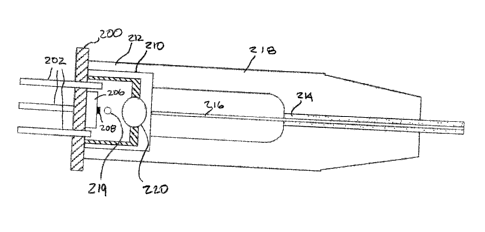
Figure 10 shows a CWDM electro-optical assembly according
to the present invention. There is a ca-ax base 200 with electrical
connectors 202: Then there is a substrate 206 onto which the laser
chip 208 is operatively connected. A connection cavity 210 is
formed by boot wall 212. A fibre assembly 214 surrounds a fibre
216 and is sized and shaped to fit into the connection cavity 210.
A boot 218 completes the mechanical connection of the fibre
assembly to the fibre itself. An optional rod lens 219 and a ball lens
220 are shown and help to couple the signal output to the fibre 216.
As will be appreciated from the foregoing description the
present invention provides for much less expensive packaging of
the signal source than was possible in the prior art. Quite simply,
the need for an isolator 16 has been eliminated, with the surface
emissions being fed directly into the fibre in the preferred
CA 02392119 2002-06-28
-18-
embodiment. The present invention comprehends the use of a lens
220 or lenses, if desired, to assist in c~upling the signal to the fibre,
depending upon the form of the signal output, and its suitability to
be easily coupled to the fibre. In this way the present invention
comprehends a simple plug and play field connection for an electro-
optical interface, where the fibre can be more closely positioned to
the signal source, and thus signals more easily and reliably coupled
thereto as compared to the prior art.
Figure 11 shows a DWDM connection according to the
present invention. In this embodiment the package base 250 may
for example be a 14-pin butterfly style base. The present invention
also comprehends other types of package base and the 14 pin
butterfly is provided by way of example only. Essentially the base
250 functions to operationally connect the electrical signals to the
electro-optical interface in such a way as to permit the electrical
signals to be converted into optical signals through the
semiconductor laser chip 252.
Connected to the package base 250 is a TEC (thermoelectric
cooler) 251 which can absorb and thus dispose of extra heat
energy, which might otherwise affect the output signal wavelength
or signal quality., A heat sink 254 is mounted to the TEC 251 and a
substrate 255 is mounted between a laser chip 252 and the heat
sink 254: The chip 252 is shown as a surface emitter of the type
previously described. The substrate operatively connects the laser
chip with the incoming electrical signals, in a known manner, which
will be understood by those skilled in the art. Adjacent to the laser
chip 256 is a fibre clip 260 of the type that can hold a fibre in place
with a metalised fibre assembly 262. A fibre 264 is shown
extending through a boot 266 into a connection cavity 268. A
removable lid 270 is provided to close the connection cavity 268.
CA 02392119 2002-06-28
-19-
As with the embodiment of Figure 10, this embodiment
requires no intervening elements between the signal emitter or chip
256 and the end of the fibre 264. All that is required is that the fibre
be adjacent to the chip, permitting the surface emissions to be
coupled to the fibre. This is referred to as operatively positioning
the fibre adjacent to the signal emitter. Again, the present invention
comprehends also the :use of a lens or lens if desired, which may
increase the manufacturing yields with the addition of a nominal
cost.
As can now be appreciated, the present invention also
comprehends a method of coupling an optical signal source to a
waveguide that includes a number of separate steps. The first step
is to provide a semiconductor laser source having a second or
higher order grating and a cavity, the cavity being sized, shaped
and positioned to produce signals within the telecommunications
band. The grating, in turn, is such as to induce surface emissions.
The grating is also designed such that the radiation field is not a
mode-selection mechanism. The next step is to operatively position
the semiconductor laser adjacent to a waveguide: Then the last
step is to couple the surface emissions of the laser to the
waveguide without any intervening isolator.
While the foregoing description has been made with respect
to various preferred embodiments it will be understood by those
skilled in the art that various modifications and alterations can be
made without departing from the broad spirit of the attached claims.
While some of these variations have been discussed above, others
will also be apparent. For example, what is important is to structure
the cavity, by shape, size and configuration in a way that a radiation .
field for said cavity is not a mode discrimination mechanism, so
back reflection into the cavity does not result in "coherence
CA 02392119 2002-06-28
'20'
collapse". The cavity may be index coupled, with a phase shift, gain
coupled, loss coupled as desired, provided the radiation field is not
a mode discrimination mechanism.