Note: Descriptions are shown in the official language in which they were submitted.
CA 02392273 2002-05-21
WO 01/39252 PCT/US00/32198
ACTIVE PACKAGE FOR INTEGRATED CIRCUIT
FIELD OF THE INVENTION
This invention relates to an active package for an integrated circuit and a
discrete
component. More particularly, the invention relates to an active package for
an'
integrated circuit in which the package comprises a discrete component as part
of the
housing for the integrated circuit.
BACKGROUND OF THE INVENTION
A typical assembled circuit, such as a PCB assembled circuit, includes an
integrated circuit individually packaged in a passive plastic or ceramic
package that
encapsulates and protects an integrated circuit, and one or more discrete
component such
as a resistor, capacitor or inductor that is assembled together with the
integrated circuit
onto a PCB circuit board. The assembled circuit, such as a power circuit,
microprocessor,
memory application, logic device, rf amplifier, etc., also generally includes
transmission
lines printed on the circuit board substrate and soldered interconnects that
lead to
parasitic losses due to the inherent resistance, capacitance and inductance of
the
transmission lines and soldered interconnects. These parasitic losses greatly
increase in
circuits that operate at high switching speeds. In order to minimize the
parasitic losses,
circuit designers have moved the circuit components closer together on the
circuit board.
Although the parasitic loss due to the transmission lines may be decreased,
placing the
components in close proximity may result in energy radiation, such as
electromagnetic or
heat, generated by one or more of the components may interfere with the
operation of
another component. In addition, higher current handling system designs face
unique
problems such as larger component size requirements due to potential
dielectric or
CA 02392273 2002-05-21
WO 01/39252 PCT/L1S00/32198
insulation breakdowns, energy storage requirements, heat dissipation, high
transmission
line losses, especially for switching converters where it affects the power
conversion
efficiency as well as voltage conversion efficiency and higher efficiency
constraints.
Power circuits, such as switching power converters, linear regulators, power
integrators, charge pumps, op amp circuits, comparator circuits, relay driver
circuits,
relay actuation circuits, power integration circuits with power monitoring and
power
control, proximity switches, etc., for example, typically include one or more
power
converting or regulation component and one or more intrinsic energy
conversion, storage
or conservation component that are individually packaged and assembled
together on a
single PCB substrate and/or inside a passive plastic or ceramic package (e.g.,
hybrid
packages). A switching converter may include a charge pump integrated circuit,
a flying
capacitor and a storage capacitor or a plurality of capacitors that make up a
flying or
storage capacitor. The various components may generate electromagnetic or heat
energy
radiation that may affect the operation of other components. In order to
dissipate the heat
generated, many power circuits include a heat sink attached to the plastic or
ceramic
package that houses the power converting or regulation component (e.g., a
T0220
standard power converter package). The total size of the package including the
heat sink
is typically at least an order of magnitude larger than the size of the
integrated circuit
itself depending upon the power dissipation, the power carrying capability and
the
number of pins required.
SUMMARY OF THE INVENTION
The present invention includes an integrated circuit package including an
active
component that is part of the circuit topology of the integrated circuit and
forms at least a
part of the housing for the integrated circuit. In one embodiment, for
example, the
integrated circuit may be housed in a shell formed by one or more discrete
components to
form an package in which the discrete component is an element of the circuit
including
the integrated circuit. The active package may be formed in the same geometry
and
2
CA 02392273 2006-O1-18
30369-5
dimensions as a standard passive integrated circuit package,
may be formed in a shape to fit inside a standard or
specially made battery package, or may be formed in a size
and shape to fit in a device or to form a part of the
chassis of the device.
In an alternative embodiment of the present
invention, a smart component may include a discrete
component or a semiconductor-based resistor, capacitor or
inductor, and a separate integrated circuit housed in the
same housing as the discrete component or a semiconductor-
based resistor, capacitor or inductor. The integrated
circuit may control at least one electrical parameter of the
discrete component or a semiconductor-based resistor,
capacitor or inductor. In one embodiment, for example, the
integrated circuit may maintain the resistance, resistivity,
capacitance, inductance, etc. of the component inside a
narrow range in order to create a high-precision component
regardless of changes in environmental changes such as
temperature, pressure, humidity, etc.
The invention may be summarized broadly as an
integrated circuit package comprising: (a) a package input
contact pad, a package output contact pad and a package
neutral contact pad; (b) a discrete component electrically
connected between the package neutral contact pad and one of
the package input contact pad and the package output contact
pad; and (c) an integrated circuit including a first side,
and a second side, an integrated circuit input contact pad,
an integrated circuit output contact pad and an integrated
circuit neutral contact pad, the integrated circuit input
contact pad electrically connected to the package input
contact pad, the integrated circuit output contact pad
electrically connected to the package output contact pad,
and the integrated circuit neutral contact pad electrically
3
CA 02392273 2006-O1-18
30369-5
connected to the package neutral contact pad; wherein the
discrete component forms a first side of the package that
protects the first side of the integrated circuit, and the
discrete component forms a heat sink.
BRIEF DESCRIPTION OF THE DRAWINGS
Figure 1 shows a schematic representation of a
power integrator circuit including a charge pump power
converter.
Figure 2 shows an alternative embodiment of a
power integrator circuit including a charge pump power
converter.
Figure 3 shows a schematic block diagram of a
power integrator circuit including a charge pump that may be
housed in an active package of the present invention.
Figure 4 shows a simplified exploded view of one
embodiment of an active package design for the power
integrator circuit shown in Figure 3.
Figure 5 shows a simplified exploded cross-
sectional view taken along section lines V-V of Figure 4.
Figure 6 shows a simplified exploded cross-
sectional view taken along section lines VI-VI of Figure 4.
Figure 7 shows a schematic representation of a
power converter circuit including a DC/DC converter.
3a
CA 02392273 2002-05-21
WO 01/39252 PCT/US00/32198
Figure 8 shows a schematic block diagram of a circuit layout for the power
converter circuit shown in Figure 7.
Figure 9 shows a simplified exploded view of an active package design of the
present invention that houses the power converter circuit shown in Figure 7.
Figure 10 shows a simplified exploded view of an active package design of the
present invention including an integrated circuit and a single discrete
component.
Figure 11 shows a sectional view taken of the active package design of Figure
10
along section line XI - XI.
Figure I2 shows a schematic representation of an audio op amp power amplifier
circuit.
Figure 13 shows an alternative embodiment of an active package design of the
present invention.
Figure 14 shows a battery including an active package design of the present
invention.
Figure 15 shows yet another embodiment of an active package design of the
present invention.
Figure 16 shows a simplified exploded view of an alternative embodiment of the
present invention.
Figure I7 shows a perspective view of an another embodiment of the present
invention.
Figure 18 shows a cut-away view of the embodiment of Figure 17.
Figure 19 shows a simplified cut-away view of an yet another embodiment of the
present invention.
Figure 20 shows a simplified exploded, cut-away view of the embodiment of
Figure 19.
Figure 21 shows a simplified perspective view of an another embodiment of the
present invention.
Figure 22 shows a simplified exploded view of a further embodiment of the
present invention.
4
CA 02392273 2002-05-21
WO 01/39252 PCT/US00/32198
DETAILED DESCRIPTION OF THE INVENTION
An active package as used in this application refers to a package for at least
one
integrated circuit and at least one discrete component that is part of the
same circuit with
the integrated circuit. The active package includes at least one discrete
component as part
of the housing for the one or more integrated circuit. An active package may
include one
or more integrated circuit along with one or more discrete component. An
integrated
circuit refers to a semiconductor chip including electronic elements
fabricated into the
chip or onto the surface of the chip (e.g., silicon, GaAs, Site, SiC). The
term discrete
component refers to a resistor, a capacitor or an inductor that is not
fabricated on an
integrated circuit. A high efficiency capacitor refers to capacitors having
relatively low
charge leakage and very low ESR (equivalent serial resistance) and low dynamic
serial
resistance, for example, double layer electrolytic capacitors (e.g.,
capacitors known as
super-capacitors, ultra-capacitors and power capacitors) and pseudo
capacitors.
A smart eempor~-~~e-lude$-~ discrete-component or, in one alternative
embodiment, a semiconductor-based resistor, capacitor or inductor having at
least one
semiconductor chip that controls at least some portion of the operation of the
discrete
component housed inside the housing of the discrete component. A smart
component
may, for example, include a controller that monitors environmental conditions
such as
pressure, temperature, humidity, etc. and optimize the performance of the
discrete
component based upon the condition. A smart component may, fox example,
provide a
single-piece precision discrete component that is able to maintain its desired
electrical
properties such as resistance, capacitance or inductance within a tight
tolerance level
regardless of changing environmental conditions. A smart component may be
transparent
to the circuit in which the discrete component is a part, or may provide an
input to the
circuit.
An assembled circuit may include discrete components that are intrinsic and/or
extrinsic to the circuit topology. As used in this application, an intrinsic
component is a
discrete component that performs a function integral with the function of the
circuit. In a
CA 02392273 2002-05-21
WO 01/39252 PCT/US00/32198
power integrator, for example, a resistor, a flying capacitor, a storage
capacitor or an
inductor perform an energy conversion, storage and/or conservation role that
is required
for the power integrator to operate as designed. An extrinsic component,
however, refers
to a discrete component that is not integral with the function of the circuit.
An extrinsic
component may be used to enhance the operation of the circuit. A filter
capacitor, for
example, may be connected between an input or output terminal and ground to
enhance
the operation of an assembled circuit, but is not required for the circuit to
operate as
designed and, as such, represents an added cost to the overall circuit design.
An active package of the present invention may significantly reduce the cost
and
complexity of packaging and assembling an integrated circuit. By using an
active
component as a housing or shell for an integrated circuit, the present
invention may
eliminate passive material otherwise required to package the integrated
circuit. In
addition, an embodiment of the present invention that uses an intrinsic
component of the
assembled circuit instead of an extrinsic component may reduce the number of
active
components used in the circuit and may correspondingly reduce the finished
cost of the
assembled circuit. Using all the intrinsic components of the assembled circuit
in the
housing or shell may also significantly reduce costs even more because the
chip
packaging and the circuit assembling may be performed in the same step. Where
the
components are able to be mechanically interconnected, the present invention
may also
allow for reduced or eliminated use of solder. This, in turn, may further
reduce costs of
assembly and allow for more environmentally-friendly products due to the
reduction or
elimination of lead used in the solder. Where the intrinsic component, such as
a flying or
storage capacitor of a power converter, may also perform a function that may
otherwise
be performed by an extrinsic component, such as a filter capacitor, this also
results in
further cost savings because the cost of the extrinsic component may be
eliminated.
An active package may also allow for a boardless design of an assembled
circuit
because the discrete components are used as the integrated circuit packaging
elements.
An active package may include multiple integrated circuits at least partially
housed in or
by a discrete component. For example, a multiple chip module may be replaced
by an
6
CA 02392273 2002-05-21
WO 01/39252 PCT/US00/32198
active package of the present invention that includes two or more integrated
circuits
housed in an active package of the present invention. Although not required,
in one
embodiment one or more integrated circuits and/or discrete components may be
assembled on a PCB board that is housed within an active package of the
present
invention.
In one embodiment of the present invention, an active package may include a
"shell" structure that includes a top shell and/or a bottom shell. In the
embodiment
including a dual-sided shell design such as the design shown in Figures 4-6
and 9, the two
shell sides may encapsulate an integrated circuit. In a single-sided shell
design, such as
shown in Figure 10 and 11, the shell side may protect one side of an
integrated circuit.
The other side of the integrated circuit may be protected by a passive
packaging material
such as plastic or ceramic material, or may be self protecting such as a flip-
chip. A shell
side may include a single discrete component that protects one side of an
integrated
circuit such as the top shell designs shown in Figures 4-6 and the bottom
shell design
shown in Figures 4-6 and 9-11. Alternatively, the shell side may comprise
multiple
discrete components that are attached together to form a single side of a
shell such as the
top shell design shown in Figure 9.
Active components used in the housing or shell may also be used as a heat sink
for the integrated circuit and, in many cases, may eliminate the need for an
external heat
sink altogether. A capacitor, a resistor or an inductor that is housed
adjacent to the
semiconductor chip may distribute and dissipate heat generated in the
semiconductor
chip more efficiently than a typical plastic or ceramic packaging material. In
addition,
the discrete component used as the housing or shell may also include a metal
casing or
layer that may further aid in dissipating heat from the active package.
Further, the
discrete components may also be conf gored so that the active package may be
attached
to a conventional heat sink. A component may, for example, include a hole
similar to
those of typical integrated circuit packaging designs that may be used to
attach the active
package to a heat sink. An active package of the present invention may also
enable an
7
CA 02392273 2002-05-21
WO 01/39252 PCT/US00/32198
integrated chip to operate at the lower temperature than typical because the
parasitic
dissipation may "warm up" the semiconductor chip.
An active package of the present invention may also allow for higher noise
immunity and may allow for use of parasitic elements as part of the circuit.
By
encapsulating a larger part, or even the entire part, of the circuit may allow
for higher
noise immunity of the circuit and may reduce the noise generated by the
circuit that
affects other nearby circuits. Also, the proximity of the semiconductor chip
to the other
components may lead to more predictable parasitic elements of the circuit that
may be
utilized in the design of the circuit.
An active package design of the present invention may also be scaleable, i.e.,
multiple active package designs may be connected together. In this embodiment,
the
combination of active package designs may allow for an interconnecting board-
less
circuit in which all the circuit elements are interconnected in one package.
In a particular
embodiment, this package may form a portion of the chassis of a device that
houses the
electronic circuitry for that device or may even form all or a portion of the
chassis of the
device.
An embodiment of the present invention may also include a discrete component
that responds to or senses an environmental condition such as pressure,
temperature,
humidity, etc., or a change in the environmental condition. The circuit may
detect this
condition or change in condition and respond by optimizing the operation of
the circuit to
maximize the performance of the circuit. The circuit component may include,
for
example, a thermistor, temperature diode, a capacitor, or an inductor that
responds to a
change in temperature by a change in the resistance, capacitance or inductance
of the
component. The circuit may detect this change and use the change as a feedback
signal to
optimize the performance of the circuit.
Any circuit having including an integrated circuit and one or more intrinsic
discrete components may be configured into an active package of the present
invention.
8
CA 02392273 2002-05-21
WO 01/39252 PCT/US00/32198
A power integrator including a charge pump integrated circuit, a flying
capacitor and a
storage capacitor, for example, includes two discrete components that may form
a shell to
house the charge pump integrated circuit. Figure 1 shows a simplified
schematic
representation of a power integrator circuit 20 including a charge pump 26, a
flying
capacitor 22 and a storage capacitor 28. In the power integrator circuit 20,
the flying
capacitor 22 is electrically connected between the input terminal 21 of the
power
integrator circuit 20 and the neutral terminal 25 of the power integrator
circuit 20. The
charge pump 26 has an input terminal 23, a neutral terminal 27 and an output
terminal 24.
The input terminal 23 of the charge pump 26 is electrically connected to the
input
terminal 21 of the power converter circuit 20. The output terminal 24 of the
charge pump
26 is electrically connected to the output terminal 29 of the power integrator
circuit 20.
The neutral terminal 27 of the charge pump 26 is electrically connected to the
neutral
terminal 25 of the power integrator circuit 20. The storage capacitor 28 is
electrically
connected between the output terminal 29 of the power integrator circuit 20
and the
neutral terminal 25 of the power integrator circuit 20.
In an alternative embodiment, the power converter circuit may include a
component that includes an environmental condition sensor or a component that
changes
parameters in response to a change in an environmental condition such as
pressure,
temperature, humidity, etc. (e.g., a capacitor that changes capacitance as the
temperature
varies). Figure 2, for example, shows an alternative embodiment of a power
integrator
circuit 30 to the power integrator circuit 20 shown in Figure 1 in which the
storage
capacitor 38 may include a temperature sensing element, and/or the capacitor
may change
capacitance as the temperature varies (alternatively, the flying capacitor may
be used to
detect a change in temperature). As the temperature of the charge pump
integrated circuit
or of the environment varies, the charge pump 26 may detect a change in the
capacitance
of the storage capacitor 38 or receive an input from the temperature sensing
element and
vary the operation of the charge pump 26 such as by changing the duty cycle of
the
converter to optimize the performance of the circuit. In this embodiment, for
example,
the utilization of a temperature sensor or a change in capacitance may allow
for better
system controller performance due to the measurable dissipation information
available as
9
CA 02392273 2006-O1-18
30369-5
feedback for real time circuit operating conditions.
Alternatively, the capacitor of this circuit may comprise a
smart-component capacitor in which the capacitor may include
an integrated circuit that monitors one or more
environmental conditions and optimizes the performance of
the capacitor to keep it in a desired range of performance.
Other power integrators incorporating a charge pump that are
known in the art may also be housed in an active package of
the present invention.
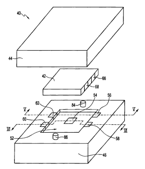
Figure 3 shows a schematic block diagram of a power
integrator circuit including a charge pump integrated circuit
42, a flying capacitor 44 and a storage capacitor 46 that may
be housed in an active package of the present invention.
Figure 4 shows a simplified exploded view of one embodiment
of an active package design 40 for the power integrator
circuit shown in Figure 3. Figures 5 and 6 show two
simplified exploded cross-sectional views taken along section
line V - V and VI - VI of Figure 4, respectively. The active
package 40 includes a power integrator with a charge pump
converter circuit having a charge pump integrated circuit 42,
a flying capacitor 44 and a storage capacitor 46. In this
embodiment, the charge pump integrated circuit 42 is located
between the storage capacitor 46, which provides a substrate
upon which the charge pump integrated circuit 42 is located
and forms one side of the active package 40 shell, and the
flying capacitor 44, which forms the second side of the
active package 40 shell. The positions of the capacitors 44
and 46 may be reversed. The flying capacitor 44 and/or the
storage capacitor 46 may include a recess, such a recesses 51
and 52, in which the charge pump integrated circuit 42 may be
partially or fully housed. The recesses) 51 and 52 may
CA 02392273 2006-O1-18
30369-5
include a dimple, a notch or a cavity or etched groove formed
in one or both of the capacitors 44 and 46. The recess(es)'
51 and 52 may be milled, etched, molded, etc.
l0a
CA 02392273 2002-05-21
WO 01/39252 PCT/US00/32198
The storage capacitor 46 and/or the flying capacitor 44 may be fully or
partially
encased by an insulator material. In one embodiment, the thickness 53 and 55
of the
insulators 49 and 50 at least on the side of one or both of the capacitors 44
and 46 that is
adjacent to the charge pump integrated circuit 42 may be calculated to prevent
an
electromagnetic or field generated either by the charge pump integrated
circuit 42 or a
capacitor 44 or 46 from extending into the other component. In this
embodiment, the
insulators 49 and 50 prevent the components that are located in close
proximity from
interfering with the operation of the other component. In this embodiment, the
flying
capacitor 44 and the storage capacitor 46 are shown to be tantalum/polymer
capacitors in
which the dielectric layers 41 and 53 may be molded in order to provide easier
connections between the electrodes 43, 45, 47 and 48 and the rest of the
circuit without
extending a pin through the dielectric layers 41 and 53 of the capacitors 44
and 46. The
capacitors may, however, be other types of capacitors known in the art such as
high
efficiency capacitors including ultra-capacitors, super capacitor, double
layer electrolytic
capacitors or pseudo capacitors. The capacitors may have terminals on the
surface of the
capacitors in order to allow for easier electrical connections of the
capacitors to the rest of
the circuit.
The charge pump integrated circuit 42 may be electrically connected to the
flying
capacitor 44 and the storage capacitor 46 by contact pads as shown in Figure
4. In this
embodiment, the neutral terminal 64 of the charge pump integrated circuit 42
is
electrically connected to the neutral pin 74 of the active package 40 by the
contact pad
54. The negative electrode 45 of the flying capacitor 44 is electrically
connected to the
flying capacitor negative terminal 66 of the charge pump integrated circuit 42
by contact
pads 56 and 80, which are brought into physical and electrical contact with
each other
when the active package 40 is assembled. The positive electrode 43 of the
flying
capacitor 44 is electrically connected to the flying capacitor positive
terminal 72 of the
charge pump integrated circuit 42 by contact pads 62 and 82, which are also
brought into
electrical and physical contact when the active package 40 is assembled.
T°he positive
input terminal 68 of the charge pump integrated circuit 42 is electrically
connected to the
positive input pin 76 of the active package 40 by the contact pad 58. The
output terminal
11
CA 02392273 2002-05-21
WO 01/39252 PCT/US00/32198
70 of the charge pump integrated circuit 42 is electrically connected to the
output pin 78
of the active package 40 by contact pad b0. The positive electrode 47 of the
storage
capacitor 46 is electrically connected to the output pin 78 of the active
package 40, and
the negative electrode 48 of the storage capacitor is electrically connected
to the neutral
pin 74 of the active package.
The active package 40 of the present invention may be assembled in a number of
different ways. The charge pump integrated circuit 42, for example, may be
soldered to
the flying capacitor 44 and/or the storage capacitor 46, may be mechanically
latched
together with the flying capacitor 44 and/or the storage capacitor 46, may be
snap fit into
a recess such as recess 51 and/or 52 by spring forces if the terminals of the
charge pump
integrated circuit 42 or the contact pads of either of the capacitors in the
recesses 51
and/or 52 include resilient members that hold the charge pump integrated
circuit 42 in
place, or may even rest in place in a recess such as recess 51 and/or 52. The
charge pump
integrated circuit 42 may alternatively be connected to the flying capacitor
44 and/or the
storage capacitor 46 by any means known in the art. The flying capacitor 44
and the
storage capacitor 46 may also be connected together in many different ways to
form an
active package 40 of the present invention. The capacitors, for example, may
be bonded
together by bonding pads such as bonding pads 84, 86, 88 and 90. The bonding
pads 84,
86, 88 and 90 are insulated from the flying capacitor 44 and the storage
capacitor 46 by
insulators 49 and 50, respectively. Thus, the bonding pads 84, 86, 88 and 90
allow for
mechanical connections between the capacitors, but not electrical connections.
Alternatively, the flying and storage capacitors 44 and 46 may be soldered,
mechanically
interconnected, or connected by any other means known in the art.
An alternative embodiment of a power converter circuit 100 including a flying
capacitor 110, an inductor 112, a DC/DC converter 114, and a storage capacitor
116 is
shown in Figure 7. Figure 8 shows a schematic block diagram of a circuit
layout for the
power converter circuit 100 shown in Figure 7, and Figure 9 shows a simplified
exploded
view of an active package 120 of the present invention that houses the power
converter
circuit 100 shown in Figure 7. In this embodiment, the flying capacitor 110
and the
12
CA 02392273 2002-05-21
WO 01/39252 PCT/US00/32198
inductor 112 mate together and form the top shell of the active package 120
(alternatively, the flying capacitor 110 and the inductor may form the bottom
shell of the
active package 120). The flying capacitor 110 and the inductor 112 may be
connected,
for example, by the interlocking posts 122 and holes 124. The posts 122 and
the holes
124 may snap-fit together or interlock by other mechanical means. The posts
122 may be
insulated from the electrodes of the flying capacitor 110 and/or the holes 124
may be
insulated from the inductor 112 if a purely mechanical connection is desired.
In this case
another form electrical contact, if needed, may be supplied. In Figure 9, for
example,
contact pads 126 on the flying capacitor 110 and the inductor 112 may be used
to make
electrical contact between the two components. Alternatively, one or more of
the posts
122 may be electrically connected to an electrode of the flying capacitor 110
and one or
more of the holes 124 may be electrically connected to the inductor 112. In
this way,
both the mechanical and electrical connections between the flying capacitor
110 and the
inductor 112 may be made by the posts 122 and the holes 124. If the discrete
components
are not to be directly electrically connected to each other, only mechanical
connections
need be made.
As shown in Figure 9, DC/DC converter integrated circuit 114 may be located in
recess 128 of storage capacitor 116. A recess may also be formed in the flying
capacitor
110, the inductor 112 to house a portion or alI of the DC/DC converter
integrated circuit
114 in addition to or instead of the recess 128 formed in the storage
capacitor 116. The
DC/DC converter integrated circuit may be electrically connected to the flying
capacitor
110, the inductor 112, the storage capacitor 116, the neutral pin 138 and the
output pin
140 by terminals 130 and contact pads 132 as described above with respect to
Figures 4-
6. The flying capacitor 110 and the inductor 112 may be electrically connected
to the
input pin 136 via contact pads 132. The top and bottom shells of the active
package 120
may be connected together by bonding pads 134 as described above.
Alternatively, the
top and bottom shells of the active package 120 may be soldered, mechanically
interconnected, or connected by any other means known in the art.
13
CA 02392273 2002-05-21
WO 01/39252 PCT/US00/32198
In an alternative embodiment, multiple resistors, capacitors or inductors may
be
connected together such as in the manner shown in Figure 9 and described
above, or by
any other method described in this application or known in the art, to form
the desired
circuit connections. In order to provide the desired resistance, capacitance
or inductance
values, for example, multiple resistors, capacitors or inductors may be
combined together
in series or in parallel. In a capacitor, for example, each post may be
electrically
connected to a different electrode of that capacitor, and each hole may be
electrically
connected to a different electrode of that capacitor. Then, the capacitors may
be
connected in series or in parallel depending upon which post was inserted into
which
hole. In addition, different types of discrete components such as the
capacitor and
inductor shown in Figure 9 may be connected together to form various circuit
configurations desired for a particular application. Figure 22 shows a
simplified
exploded view of yet another embodiment of the present invention in which
multiple
discrete components 1010 may be mated together to form a single shell side
1020 that
forms the top of an active package of the present invention including
integrated circuit
1012 and Garner 1014. The connections shown may be snap fit configurations in
which
no solder is necessary and may also include purely mechanical connections in
which the
electrical elements of the discrete components are insulated from each other,
or may also
include electrical connects between the discrete components.
Yet another embodiment of an active package of the present invention is shown
in
Figures 10 and 11. Figure 11 shows a sectional view taken along section line
XI - XI
shown in Figure 10. In this embodiment, the active package 200 includes an
integrated
circuit 210 and a single discrete component 220. In this embodiment, the
integrated
circuit 210 could be designed with the exposed side of the integrated circuit
210
protected, such as a flip-chip design (e.g., wafer scale packaging).
Alternatively, the
active package 200 could include a passive packaging material such as plastic
or ceramic
that covers the exposed side 212 of the integrated circuit 210. The electrical
and
mounting connections between the integrated circuit 210 and the discrete
component 220
may be any of the methods described above or any other connections known in
the art.
Figure 11, for example, shows an exemplary electrical contact pad 224 that
extends
14
CA 02392273 2006-O1-18
30369-5
through insulator layer 222 of the discrete component 220.
Discrete component 220 may be one or more capacitor,
inductor and/or resistor or a combination of one or more
capacitor, inductor and/or resistor. An example of a
circuit that may be housed in an active package 200 design
that includes a single discrete component is an audio op amp
power amplifier circuit. A circuit schematic for an audio
op amp power amplifier circuit that may be housed in an
active package design such as the active package design 200
is shown in Figures 12.
Battery Top
In an alternative embodiment, a power converter,
regulator or charge pump circuits may be housed in an active
package design of the present invention that is designed to
fit under a false positive top or a false negative bottom of
a battery. As shown in Figure 13, for example, a charge
pump active package 300 is designed to fit under the false
positive top of a cylindrical battery (e.g., AA, AAA, C
or D). In this embodiment, the storage capacitor 314, being
the larger capacitor, forms the base of the active
package 300 and provides a substrate on which a converter,
regulator or charge pump integrated circuit, such as the
charge pump integrated circuit 312, may be located. The
flying capacitor 310 is narrower than the storage capacitor
314 and forms the top of the active package 300. As shown
in Figure 14, the narrower top of the active package 300 may
be designed to fit within the dimple 324 of a false positive
top 322 of a standard cylindrical battery 320.
Alternatively, the shape of the active package 300 may be
designed to fit in another location of a standard
cylindrical battery or in another battery such as a
prismatic, or other type of battery. Designs of power
converters, regulators or charge pump circuits that may be
CA 02392273 2006-O1-18
30369-5
used in the package of the present invention are described
in United States Patents 6,198,250; 6,118,248; 6,163,131;
6,074,775: 6,835,491: and 6,483,275.
In one embodiment, the flying capacitor 310 and
the storage capacitor 314 may be high efficiency capacitors
such as the ultra-capacitor coin cells described in Table 1
below. The ultra-capacitor coin cells may include two
terminals on the same side of the capacitor in order to
allow for easier connection in an active package of the
present invention such as this embodiment or in other
embodiments disclosed in the application.
Table 1
Technical Parameters Flying Capacitor Storage Capacitor
Capacitance 0.05F (-10~, +25~) 1F (-10$, +25%)
Series Resistance (25C):
DC <0.09 Ohms <0.10 Ohms
100 HZ <0.08 Ohms <0.08 Ohms
Voltage:
Continuos Voltage 2.8 V 2.8 V
Peak Voltage 3.6 V 3.6 V
Dimensions 4 mm OD; 2 mm 6.5 mm OD; 2.5 mm
height height
Temperature
Operating -20C to +60 C -20C to +60C
Storage -40C to +80C -40C to +80 C
Leakage Current (after 0.01 to 0.02 mA 0.005 to 0.01 mA
72 Hrs)
16
CA 02392273 2002-05-21
WO 01/39252 PCT/US00/32198
In one embodiment of the present invention, the active package may be formed
into a standard integrated circuit package, such as a surface-mounted or wafer-
scale
package, in which one or more intrinsic components are incorporated into the
active
package in the same geometry as the standard integrated circuit package. In
this way, the
active package may replace all or part of the circuit that a standard passive
package is
used.
As shown in Figure 22, multiple discrete components may be mated together to
form a
shell side of an active package of the present invention. In this embodiment,
discrete
components 1010 are mated together to form the top shell side 1020 of the
active package
1000 such as for a microprocessor integrated circuit package. This top shell
side 1020
may replace the passive package material of a typical microprocessor
integrated circuit
package (e.g., BGA-256) and allow for discrete components typically placed on
a PCB
board to be integrated into an active package 1000 of the present invention.
The bottom
carrier 1014 may include a typical pin carrier (e.g., BGA-256).
In on particular embodiment, the active package may include a fully integrated
charge pump that is in a standard charge pump package form. The active package
may be
formed into a TO-220, SOT-223, TO-3, T092, T087, etc. standard form. Figure
15, for
example, shows an embodiment in which the active package is formed into a TO-
220
standard form package. In this embodiment, the flying capacitor 410 and the
storage
capacitor 414 form the top and the bottom halves of the housing shell that
encapsulates
the integrated circuit 412. The flying capacitor 410 may be the same
dimensions as the
top of a standard TO-220 package. In the embodiment shown in Figure 15, the
storage
capacitor 414 forms only a portion of the bottom half of the TO-220 package,
and a
metal, plastic or ceramic tab is attached to the storage capacitor to complete
the bottom
half of the standard package and to allow the package to be connected to a
heat sink. In
an alternative embodiment, the storage capacitor may be the same dimensions
the bottom
of a standard TO-220 package and may, if necessary, include a hole that allows
for
attachment of the package to a heat sink. In one embodiment, the flying
capacitor 410
17
CA 02392273 2002-05-21
WO 01/39252 PCT/US00/32198
and the storage capacitor 412 may be high efficiency capacitors such as the
ultra-
capacitors described in Table 2 below.
Table 2
Technical Parameters Flying Capacitor Storage Capacitor
Capacitance 0.05 F (-10%, +25%)1F (-10%, +25%)
Series Resistance (25C):
DC
<0.09 Ohms <0.10 Ohms
100 HZ <0.08 Ohms <0.08 Ohms
Voltage:
Continuous Voltage 2.8 V 2.8 V
Peak Voltage 3.6V 3.6V
Dimensions 8.38 mm x 10.16 26 mm x 10.16 mm x
mm x 2.45
2mm to 2.65 mm
Temperature
Operating -20 C to +60 C -20 C to +60 C
Storage -40 C to +80 C -40 C to +80 C
Leakage Current (after0.01 to 0.02 mA 0.005 to 0.01 mA
72 hrs)
Figure 16 shows a simplified exploded view of an alternative embodiment of the
present invention that may be used to replace a standard TO-3 package. The
active
package includes flying capacitor 510, integrated circuit 512 and storage
capacitor 514.
Figure 17 shows a perspective view of an another embodiment of the present
invention including discrete components 610 and 614, and integrated circuit
612. Figure
18 shows a cut-away view of the embodiment of Figure 17.
Figure 19 shows a simplified cut-away view of an yet another embodiment of the
present invention. In this embodiment, the active package includes discrete
components
18
CA 02392273 2002-05-21
WO 01/39252 PCT/US00/32198
810 and 814, and integrated circuit 812. Figure 20 shows a simplified
exploded, cut-
away view of the embodiment of Figure 19.
Figure 21 shows a simplified perspective view of an another embodiment of the
present invention including a smart component. The smart component is shown
without
its housing and shows component 910, which may be a discrete component or a
semiconductor component such as a silicon based resistor, capacitor or
inductor.
19