Note: Descriptions are shown in the official language in which they were submitted.
CA 02392404 2002-05-22
WO 01/38922 PCT/US00/32166
ANALOG OPTICAL SWITCH USING
AN INTEGRATED MACH-ZEHNDER INTERFEROMETER
HAVING A MOVABLE PHASE SHIFTER
FIELD OF THE INVENTION
The present invention is directed to small-scale Mach-Zehnder interferometer
("MZI")
devices and structures. The present invention is also directed to analog
optical switches.
BACKGROUND OF THE INVENTION
An optical network, in its simplest representation, consists of an optical
source, a
destination, and a matrix of devices (e.g., fiber-optical cables, waveguides,
cross-connects,
amplifiers, etc.) for causing an optical signal generated by the source to
reach a desired
destination. Physical and geographic boundaries present no impediment to
telecommunication, data communication and computing, all of which may utilize
all or part
of an optical network. Consequently, the number or sources and destinations,
and the
combinations of sources and destinations and the communication paths
therebetween, may be
nearly infinite. Optical switches are used in the optical network for
facilitating the routing of
an optical signal to its desired destination.
By way of example, FIG. 1 depicts a block diagram of a part of an optical
component
1 comprising a plurality of optically interconnected optical devices 3 (e.g.,
switches, filters,
etc.), shown in FIG. 1 as switches. As used herein, the terms "optical
component" and
"component" refer to any and all of a plurality of interconnected devices
which may operate
using any combination of optical, opto-electrical, and/or electrical
technologies and which
may be constructed as an integrated circuit. Devices 3 can be optically
interconnected by
waveguides S. Various other optical, opto-electrical, and/or electrical
devices may also be
included in the optical component, as a matter of design choice. As used
herein, the terms
"optical", "opto-electrical", and "electrical" devices may include, by way of
non-limiting
example, lasers, waveguides, couplers, switches, filters, resonators,
interferometers,
amplifiers, modulators, multiplexers, cross-connects, routers, phase shifters,
sputters, fiber-
CA 02392404 2002-05-22
WO 01/38922 PCT/US00/32166
-2-
optic cables, and various other optical, opto-electrical, and electrical
devices. The optical
component 1 and devices 3 depicted in FIG. 1 are merely illustrative.
Although a single wavelength of light can be transmitted through the network,
in
order to increase the network's data-carrying capacity it is preferable to
transmit multiple
wavelengths of light at the same time. This is currently accomplished using
techniques
known as wave-division-multiplexing ("WDM"), dense WDM ("DWDM"), and ultra-
dense
wave-division-multiplexing ("UDWDM").
The ability to separate one optical signal from a plurality of optical signals
(or one
wavelength from a plurality of wavelengths in an optical signal) propagating
within an optical
network becomes more important as the number of signals transmitted through a
single
optical f ber (or waveguide) increases. As optical transmission evolves from
WDM to
DWDM to UDWDM, and beyond, more and more data contained in a mufti-wavelength
optical signal is transmitted over the optical network. Optical filters are
one component that
may be used to extract a desired signal (i.e., a desired wavelength) at a
particular point or
location in the network and route that signal to its desired destination,
while also permitting
other signals to continue along the network.
Optical networks transmit data as pulses of light through waveguides in a
manner
similar to electrical networks, which send pulses of electricity through
wiring. Transmitting
an optical signal between waveguides, which may occur in various devices
employed in an
optical network, may require the optical signal to leave one waveguide and
propagate through
one or more materials (mediums) before entering another waveguide. It is
likely that at least
one of the devices will have an index of refraction different than the index
of refraction of the
waveguides (which typically have approximately the same refractive index). It
is known that
the transmission characteristics of an optical signal may change if that
signal passes through
materials (mediums) having different indices of refraction. For example, a
phase shift may be
introduced into an optical signal passing from a material having a first index
of refraction to a
material having a second index of refraction due to the difference in velocity
of the signal as
it propagates through the respective materials and due, at least in part, to
the materials'
CA 02392404 2002-05-22
WO 01/38922 PCT/US00/32166
-,
respective refractive indices. As used herein, the term "medium" is intended
to be broadly
construed and to include a vacuum.
If two materials (or mediums) have approximately the same index of refraction,
there
is no significant change in the transmission characteristics of an optical
signal as it passes
from one material to the other. Accordingly, one solution to the mismatch of
refractive
indices in an optical switch involves providing an index matching or
collimation fluid to
offset any difference in refractive indices. Consequently, the optical signal
does not
experience any significant change in the index of refraction as it passes from
one waveguide
to another.
An example of this approach may be found in international patent application
number
WO 00/25160. That application describes a switch that uses a collimation
matching fluid in
the chamber between the light paths (i.e., between waveguides) to maintain the
switch's
optical performance. The use of an index matching fluid introduces a new set
of design
considerations, including the possibility of leakage and a possible decrease
in switch response
time due to the slower movement of the switching element in a fluid.
In addition, the optical signal will experience insertion loss as it passes
between
waveguides. A still further concern is optical return loss caused by the
discontinuity at the
waveguide input/output facets and the trench. In general, as an optical signal
passes through
the trench, propagating along a propagation direction, it will encounter an
input facet of a
waveguide which, due to physical characteristics of that facet (e.g.,
reflectivity, verticality,
waveguide material, etc.) may cause a reflection of part (in terms of optical
power) of the
optical signal to be directed back across the trench (i.e., in a direction
opposite of the
propagation direction). This is clearly undesirable because the reflected
signal will interfere
with the optical signal propagating along the propagation direction.
Reflection of the optical signal back across the trench also can create
problems if the
facets not only are coaxial, but also are parallel to one another. That
arrangement forms a
Fabry-Perot resonator cavity, which, under the appropriate circumstances,
allows for
resonance of the reflected signal, in known fashion.
CA 02392404 2002-05-22
WO 01/38922 PCT/US00/32166
-4-
Size is also an ever-present concern in the design, fabrication, and
construction of
optical components (i.e., devices, circuits, and systems) for use in optical
networks. It is
strongly desirable to provide smaller optical components so that optical
devices, circuits, and
systems may be fabricated more densely, consume less power, and operate more
efficiently.
Currently, optical switches can be constructed using a directional coupler or
a Mach-
Zehnder interferometer ("MZI"), as is generally known in the art. Mach-Zehnder
interferometers are known devices which take an input optical signal, split
the signal in half
(generally, in terms of optical power), direct the split signals along
different optical paths,
apply a phase shift to one of those split signals, recombine the signals and
then feed those
combined signals as a single signal to an output. The amount by which the
phase of one of
the signals is changed will, in known fashion, affect the nature of the output
signal.
Conventional Mach-Zehnder interferometers shift the phase of light traveling
along
one of the interferometers in one of several ways. If the electro-optic effect
is used, one of the
interferometer arms is made from a medium having an index of refraction which
changes in
the presence of an applied electrical field. Similarly, if the electro-thermal
effect is used, the
interferometer has an arm made from a medium having an index of refraction
that changes as
the temperature of the material changes. In each of these devices, changing
the index of
refraction of one of the interferometer arms is comparable to changing that
arm's optical
length, and results in a relative phase shift between the two split signals.
In another known
type of MZI, one of the two interferometer arms is actually longer (and thus,
optically longer)
than the other, and this also results in a relative phase shift between
signals propagating in
each arm.
In the electro-optic and electro-thermal type devices, the conditions for
effecting
optical switching in a device using a MZI, which operates by introducing a
phase shift of up
to ~ (i.e., 180°) into at least a part of the optical signal, are
defined by the equation:
~~=~z= ~ OnL (1)
CA 02392404 2002-05-22
WO 01/38922 PCT/US00/32166
-S-
where ~~ is the maximum possible phase shift of ~, ~, is the wavelength of the
optical signal
propagating in the device, L is the actual length of the device, and ~n is the
change in
refractive index effected by the application of a carrier signal, electrical
field, or change in
temperature to the device. Since the change in refractive index typically
achievable for
current optical devices is on the order of approximately 10'3, the actual
length of the device
needed to introduce a maximum phase shift of ~ must be at least 1 mm, and
preferably longer.
However, to achieve large-scale density integration, the actual length L must
be reduced
without sacrificing the ability to effect a r phase shift in an optical
signal. Those two
requirements are mutually exclusive.
If the phase is to be applied using a MZI device having different length arms,
the light
traveling through the longer arm has its phase shifted relative to the light
passing through the
other arm. Because of the difference in arm lengths, this technique cannot be
used to make
compact optical switches.
There exists a genuine need in the art for compact optical switches that can
effect a 0-
~ phase shift and which overcome the above-described shortcomings of the prior
art.
Preferably, such switches would combine small size and high actuation speed
with low power
consumption.
SUMMARY OF THE INVENTION
The present invention is directed to an analog optical switch having a MZI
with a
moveable phase shifter in one interferometer arm suitable for use in an
optical network.
More particularly, this invention is directed to improved analog M x M
switches
which employ Mach-Zehnder interferometers to control optical signals. As
already
explained, MZI devices operate by dividing an input optical signal into two
signals, applying
a phase shift to just one of those signals, and then recombining the two
signals. The output
will depend upon the magnitude of the phase shift applied. As noted
previously, known
CA 02392404 2002-05-22
WO 01/38922 PCT/US00/32166
-6-
switches of this type are larger than desired because the MZI devices used
therein operate
using techniques which thwart miniaturization.
Switches according to the present invention differ from knovm optical switches
because of the unique MZI provided in accordance with the present invention. A
MZI
constructed in accordance with embodiments of the present invention includes a
phase shifter
in one interferometer arm. The phase shifter is selectively moveable into and
out of an
optical path defined by and through the interferometer arm so as to introduce
a predetermined
phase shift into an optical signal propagating in and through that
interferometer arm. This
arrangement dramatically reduces the size of the MZI as compared with
conventional optical
switches, which may employ the electro-optic, electro-thermal or asymmetric
arms to
introduce a phase change in an optical signal. A MZI using a phase shifter in
accordance with
this invention is far more compact than a MZI which uses those known
techniques.
The present invention is particularly applicable to optical switches that are
formed on
integral planar optical substrates. Generally speaking, an integrated planar
optical substrate
refers to a relatively flat member having a supporting substrate and a number
of layers of
different materials formed thereon. The substrate and the different materials
have particular
optical qualities so that optically useful structures such as waveguides can
be formed on the
supporting substrate by suitable shaping or other processing. Such optical
switches may be
more compact and more rapidly actuated than comparable known devices.
As explained in greater detail below, this invention involves phase shifters
constructed
using small-scale fabrication techniques. This invention also encompasses
phase shifters
made using other fabrications techniques which result in comparable devices.
The present invention takes advantage of the extremely small mechanical
actuators
which can be assembled using small-scale fabrication techniques, and so
significantly reduces
the room needed on a chip for optical switches. These more compact switches
require less
chip space and so provide for denser integration of a plurality of optical
devices in an optical
component. This invention also takes advantage of the strong photon
confinement properties
of small-scale waveguides, such as are disclosed in U.S. Patent Numbers
x,878,070 and
CA 02392404 2002-05-22
WO 01/38922 PCT/US00/32166
_7_
5,790,583. Together these developments facilitate construction of optical
devices that
provide the benefits and advantages of the present invention.
One embodiment of the present invention involves a Mach-Zehnder interferometer
having a single input, a single output, and first and second arms extending
along an optical
path direction of the interferometer. One arm has a phase shifter disposed
therein. When the
phase shifter is actuated an optical signal propagating through the arm having
the phase
shifter will experience a phase shift relative to an optical signal
propagating through the other
In accordance with the present invention, a MZI may be constructed with a
selectively
moveable phase shifter in one interferometer arm. That phase shifter may be
moved into and
out of an optical path defined by and through that interferometer arm so as to
introduce a
phase shift into an optical signal propagating in and through that arm. In so
doing, the phase
shifter changes the optical length of that arm, when compared with the optical
length of the
other interferometer arm. The phase shifter may be generally wedge-shaped,
rectangular,
square, stepped (on one or both sides), or other shapes, provided that such
shapes may be
utilized to introduce a phase shift into the optical signal.
While it is generally known to provide a MZI as an element of an optical
switch, a
MZI constructed in accordance with the embodiments of the present invention
provides
significant advantages over prior art MZI devices and optical switches. For
example, the
micron-scale of the MZI enables construction of smaller optical switches that
consume less
on-chip real estate. The power requirements of the MZI to effect a desired
phase change in an
optical signal are also significantly reduced when compared with prior art MZI
devices.
The invention accordingly comprises the features of construction, combination
of
elements, and arrangement of parts which will be exemplified in the disclosure
herein, and
the scope of the invention will be indicated in the claims.
CA 02392404 2002-05-22
WO 01/38922 PCT/US00/32166
_g_
BRIEF DESCRIPTION OF THE DRAWINGS
In the drawing figures, which are not to scale, and which are merely
illustrative, and
wherein like reference characters denote similar elements throughout the
several views:
FIG. 1 is a schematic block diagram of a 1 x 16 switch that is part of a high-
density
optical component;
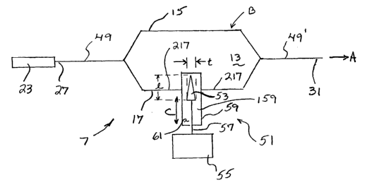
FIG. 2 is a schematic diagram of a 1 x 1 optical switch having a Mach-Zehnder
interferometer constructed in accordance with the present invention;
FIG. 3 is a schematic diagram of a 2 x 2 optical switch having a Mach-Zehnder
interferometer constructed in accordance with the present invention;
FIG. 4 is a cross-sectional view of a photonic-wire waveguide;
FIG. SAis a perspective view of a phase shifter constructed in accordance with
an
embodiment of the present invention; FIG. 5B is a cross-sectional view taken
along line SB-
SB of FIG. 5A;
FIG. 6 is a cross-sectional view showing an alternate configuration to that
shown in
1 S FIG. 5B;
FIGS. 7A and 7B are top schematic views showing a phase shift element
positioned
out of and in an optical path defined by and through two waveguides;
FIG. 8 is a top view of a tapered phase shift element constructed in
accordance with
an embodiment of the present invention;
FIG. 9A is a top cross-sectional view of an alternate embodiment of a phase
shift
element constructed in accordance with the present invention;
FIG. 9B is a top cross-sectional view of still another embodiment of a phase
shift
element constructed in accordance with the present invention;
FIG. 9C is a front elevational view of the phase shift element viewed of FIG.
9A as
viewed along line 9-9;
FIGS. 10A and l OB are schematic views showing ways to reduce diffraction of
light
passing between waveguides;
CA 02392404 2002-05-22
WO 01/38922 PCT/US00/32166
-9-
FIG. 11 is a schematic view showing offset waveguides arranged about a phase
shift
element;
FIG. 12 is a schematic view showing waveguides with angled facets;
FIGS. 13A and 13B depict the assembly of an optical switch in accordance with
an
embodiment of the present invention
FIGS. 14A and 14B show the relationship between light beam diffraction and
trench
width for light passing across a trench between waveguides; and
FIGS. 15A and 15B are partial side cross-sectional views showing portions of
the
structure of optical switches in accordance with the present invention
manufactured using
flip-chip and monolithic fabrication techniques, respectively, together with
external
components and connecting hardware.
DETAILED DESCRIPTION OF THE
PRESENTLY PREFERRED EMBODIMENTS
The present invention is directed to optical devices employing a Mach-Zehnder
interferometer ("MZI") device having a phase shifter provided in one
interferometer arm.
The present invention enables the construction of significantly smaller
optical devices than
typical photonic devices, and significantly reduces the amount of on-chip real
estate occupied
by such devices, while not affecting the ability of such devices to introduce
a predetermined
phase shift in an optical signal.
The present invention takes advantage of the extremely small mechanical
actuators
which can be fabricated using small-scale fabrication techniques, and so
significantly reduces
the room needed on a chip for optical switches. These more compact switches
require less
chip space and so provide for denser integration of a plurality of optical
devices in an optical
component.
As used herein, an "analog switch" is a switch having more than two output
states.
The term "light" as used herein should be construed in the broadest possible
sense. For
example, the term "light" is intended to include visible electromagnetic
radiation, as well as
infrared and ultraviolet radiation. The term "waveguide", as used herein,
refers generally to a
CA 02392404 2002-05-22
WO 01/38922 PCT/US00/32166
-10-
photonic-well or photonic-wire structure that provides strong photon
confinement. The term
waveguide is not intended as a limitation on the construction, shape,
materials, functionality,
or any other aspect of the optical device of the present invention, but merely
as a general
reference.
Referring now to the drawings in detail, and with initial reference to FIG. 2,
a Mach-
Zehnder interferometer (MZI) 13 is used to construct a 1 x 1 optical switch 7.
The switch 7
may receive at an input 27 an optical signal input via an input waveguide 49
and from an
optical source 23, which by way of example and not limitation may include a
laser, fiber-optic
cable, or other upstream (along the optical path direction) light generating
or light
propagating device or system. The optical signal may be a single- or mufti-
wavelength signal.
An output 31 via output waveguide 49' is controllable by the MZI 13, as
described in more
detail below.
The MZI 13 has first and second arms 15, 17 optically connecting the input 27
through input waveguide 49 to output waveguide 49' and the output 31. Light
travels along
an optical path defined by and through the input and output waveguides 49, 49'
and the MZI
arms 15, 17 in a direction generally indicated by arrow A in FIG. 2. In
contrast to known
MZI devices, present invention provides a phase shifter 51 in one MZI arm to
introduce a
phase shift into an optical signal propagating in and through that arm and
thus control the
output 31 of the MZI 13 and an optical switch 7 that includes the inventive
MZI 13.
With continued reference to FIG. 2, the optical signal traveling along input
waveguide
49 splits approximately and preferably equally (in terms of signal amplitude
or power) to each
of the first and second arms 15, 17 of the MZI 13. After passing through each
of the first and
second arms 15, 17, the divided optical signal is recombined and then
transmitted along
output waveguide 49' to output 31.
Notwithstanding the unique construction of the phase shifter formed in the
second arm
17 provided by the present invention and described below, the MZI 13 of the
present
invention functions in a fashion similar to other Mach-Zehnder devices. For
example, a
phase shift ranging from approximately 0° to approximately 180°
(~) may be introduced into
CA 02392404 2002-05-22
WO 01/38922 PCT/US00/32166
-11-
an optical signal propagating in the interferometer's second arm 17 when the
phase shifter is
actuated to alter the phase of light traveling through that second arm 17, and
this will
determine how light is output from the switch 7. The mechanism through which
such a 1 x 1
MZI switch routes light passing from the input to the output paths is known,
and so need not
be described.
In accordance with the present invention, a phase shifter 51 is provided in
one
interferometer arm 17 (which arm is a routine matter of design choice). With
continued
reference to FIG. 2, and with additional reference to FIGS. 5A and SB, one
embodiment of
the phase shifter 51 of the present invention will now be described in detail.
The
interferometer arm 17 in which the phase shifter 51 is provided is non-
continuous, although
defining a continuous optical path. Thus, that interferometer arm 17 comprises
two
waveguides 117, 217, separated by a region or trench 59 within which is
provided the phase
shifter 51. An optical signal propagating in and through the interferometer
arm 17 will pass
through phase shifter 51 or not, depending upon whether phase shifter 51 is
positioned in or
out of the optical path defined by and through that waveguide 117, trench 59
and waveguide
217. When the phase shifter 51 is positioned in the optical path, the phase of
an optical signal
propagating in and through interferometer arm 17 may be changed, depending
upon the
position and construction of the phase shifter 51, as described in more detail
below.
In one embodiment of the present invention, depicted in FIGS. 1, 5A, 5B and 6,
the
phase shifter 51 comprises a tapered or wedge-shaped phase shift element 53
connected to an
actuator 55 by a link 57. That actuator 55 and link 57 may cause selective
movement of the
phase shift element 53 into and out of the optical path, thus changing the
phase of an optical
signal propagating in and through interferometer arm 17 (and waveguides 117,
217). For
example, when the phase shift element 53 is positioned as depicted in FIG. 7A
(i.e., out of the
optical path), an optical signal propagating in and through the interferometer
arm 17 will pass
from waveguide 117 to waveguide 217 across trench 59 without experiencing a
phase shift.
On the other hand, when the phase shift element 53 is positioned as depicted
in FIG. 7B, the
optical signal will experience a phase shift, the amount (in degrees, for
example) will depend,
CA 02392404 2002-05-22
WO 01/38922 PCT/US00/32166
-12-
at least in part, on the position of the phase shift element 53 and the width
of the element 53
encountered by the optical signal.
If desired, phase shifter 51 could be arranged so that actuator 55 is disposed
between
arms 15, 17.
Generally, phase shift element 53 is constructed of optically transparent
material such
as, for example, silicon. The element 53 preferably has certain optical
qualities, in particular,
a refractive index different from that of the waveguides 117, 217 and from the
medium
provided in the trench 59, which may be air or a vacuum, for example. Light
passing between
the waveguides 117, 217 and through the phase shift element 53 will experience
a change in
velocity and thus a phase shift due to the difference in refractive indices.
Since the phase of
light passing through phase shift element 53 is affected by both the phase
shift element's
index of refraction and its width, these values can be selected to impart the
desired phase
shift(s). It is presently preferable for the phase shift element 53 to
introduce a phase shift
ranging from approximately 0° when the element 53 is not in the optical
path, to
approximately 180° (~) when the element 53 is in the optical path 53.
For a tapered or
wedge-shaped element 53, such as depicted in FIG. 2, a range of phase shifts
may be selected,
depending upon the size and shape of the element 53. Alternative embodiments
of the phase
shift element 53 in accordance with the present invention may also provide a
range of phase
shift values (see, e.g., FIGS. 9A - 9C).
With continued reference to FIGS. 2 and 6A, phase shift element 53 is
preferably
tapered, or wedge-shaped with a height h sufficient to completely intercept
and thereby shift
light passing between waveguides 117 and 217 when the phase shift element 53
is positioned
in the optical path.
The phase shift element 53 has a length 1 that is preferably minimized to
reduce the
distance by which the phase shift element 53 is moved between the first and
second positions
(i.e., positions in and out of the optical path, for example), or the distance
by which the
element 53 is moved to change the phase shift from one value to another. The
minimized
CA 02392404 2002-05-22
WO 01/38922 PCT/US00/32166
-13-
length I may also reduce the power needed to cause the phase shift element 53
to move into
and out of the optical path and improves the switch's response speed.
Tapered phase shift element 53 preferably has a maximum width t. Since the
width t
of the phase shift element 53 directly affects the insertion loss through the
MZI 13 and switch
7, a thinner phase shift element 53 may be preferred. Optical loss of light
due to light
diffraction in the trench 59, also can be minimized by having the smallest
possible phase shift
element width t.
With continued reference to FIG. 2, a preferred construction of an MZI 13 and
switch
7 in accordance with the present invention will now be discussed in detail,
The switch 7 and
MZI 13 are generally constructed as waveguides, such as depicted in FIG. 4,
which depicts an
illustrative, non-limiting cross-sectional representation of a strongly
confined waveguide 35.
The waveguide 35 is constructed on a substrate 37 and is comprised of a
relatively high (e.g.,
n = 3.5) refractive index core 39 surrounded on at least two sides (in the
horizontal direction
in FIG. 4) by a relatively low refractive index medium 41 such as air. The
core 39 is
sandwiched between upper and lower cladding layers 43, 45.
The present invention contemplates waveguides constructed in lithium niobate,
silica/glass, and other semiconductor materials provided that strong
confinement (at least in
the horizontal direction in FIG. 4) is achieved.
With continued reference to FIG. 4, the waveguide 35 there depicted in cross-
section
may comprise either a photonic-well or a photonic-wire waveguide. Exemplary
photonic-
wire and photonic-well devices are respectively disclosed in U.S. Patent Nos.
5,878,070 and
5,790,583, the entire disclosure of those patents being incorporated by
reference herein. The
waveguide 35 can be formed of semiconductor materials for on-chip integration
with other
devices such as a semiconductor laser . A wafer epitaxial growth process, or
other now
known or hereafter developed semiconductor fabrication process, may be used to
form the
various semiconductor layers of the waveguide 35 on the substrate 37. As
depicted in FIG. 4,
a lower cladding layer 45, preferably of Si02, is formed on the substrate 37,
preferably silicon
(e.g., Si) or quartz. A core 39 is formed on the first cladding layer 45 and,
by way of non-
CA 02392404 2002-05-22
WO 01/38922 PCT/US00/32166
-14-
limiting example, can be made from Si02. An upper cladding layer 43 , also
preferably of
SiO~, is formed on the core 39.
For a photonic-wire construction, the refractive index of the core 39 is
generally
greater than that of all of the upper and lower cladding layers 43, 45, and
the surrounding
medium 41. In a photonic-wire waveguide 35, the upper and lower cladding
layers 43, 45
have a very low refractive index as compared to the refractive index of the
core 39 and thus
strongly confine photons in all directions about the waveguide core 39.
Typical low
refractive index mediums for use in practicing the present invention have
refractive index
below about 2.0, preferably below 1.~, such as from about 1.5 to about 1Ø
The ratio of the
refractive indices between the core 39 and each of the upper and lower
cladding layers 43, 45
and the surrounding medium 41 is preferably larger than about 1.3.
For a photonic-well construction, the refractive index of the core 39 is
generally
greater than that of the surrounding medium 41, with the upper and lower
cladding layers 43,
45 having a refractive index close to that of the core 39 and thus weakly
confine photons
within the waveguide 35 in the vertical direction. However, strong lateral
confinement is still
provided by the difference between refractive index of the core 39 and the
relatively low
refractive index cladding medium 43, 45 laterally surrounding the core 39. In
a photonic-well
waveguide 35, the cladding layers 43, 45 may have a refractive index of about
3.17 as
compared to the refractive index of 1 for air or of 1.5 for silica. The
refractive index of
cladding layers 43, 45 is slightly less than the refractive index of core 39,
which is preferably
about 3.4.
Presently it is believed that silica-based (Si02) materials are thought to be
preferable
for constructing waveguides for the various embodiments of the present
invention. In
particular, core 39 might include germanium oxide doped silica deposited atop
a silica
substrate 37, while cladding 43 and 45 may include boron-phosphine doped
silica glass.
Other materials which could be used for the core 39 include indium phosphide
and gallium
arsenide, and the cladding 43, 45 could be made with indium phosphide, gallium
arsenide,
aluminum oxide, silicon nitride or polymers, or some combination thereof.
CA 02392404 2002-05-22
WO 01/38922 PCT/US00/32166
-15-
The core 39 can be rectangular, with sides running from approximately 3-10 pm
thick
and approximately 3-15 qm wide. More preferably, the core 39 is square, with
sides from
approximately 6-8 qm thick and approximately 6-14 ~m wide. The upper and lower
cladding
layers 43, 45 adjacent to core 39 can be approximately 3-18 ~m thick, and are
preferably
approximately 15 ~m thick.
The present invention will work with both weakly-confined waveguides and
strongly-
confined waveguides. Presently, use with weakly-confined waveguides is
preferred.
Referring next to FIG. 3, a 2 x 2 optical switch 7 having two branches 9, 11
and
constructed in accordance with another embodiment of the present invention is
depicted. The
switch 7 includes a MZI 13 having first and second arms 15, 17 optically
connecting an input
coupler 19 and an output coupler 21 along an optical path direction of the
switch 7, generally
indicated by arrows A and B. The couplers 19, 21 depicted in FIG. 3 may be co-
directional, 3
dB couplers, by way of non-limiting example. Alternatively, Y-branches or
mufti-mode
interferometer (MMI) couplers may be provided, as a routine matter of design
choice.
1 S The switch 7 may receive an optical signal input from either one of two
optical
sources 23, 25, each of which may, by way of example only, and not in a
limiting sense,
include a laser, fiber-optic cable, or other upstream (along the optical path
direction) light
generating or light propagating device or system. A first optical signal may
be directed into
an input 27 of the switch 7 by first optical source 23. The first optical
signal may comprise a
single- or mufti-wavelength signal, and as explained hereafter may be
selectively switched in
a known manner to either output 31 or 33. Similarly, and alternatively, a
second optical
signal may be directed into an input 29 by a second optical source 25, and may
also be
selectively switched to either of output 31 or 33. The optical signal output
from the switch 7
via outputs 31 and 33 are sine and cosine functions of wavelength,
respectively (as described
in greater detail below), and thus are complementary.
With continued reference to FIG. 3, an optical signal from an optical source
25 or 27
may pass through an input coupler 19 which functions as a 50:50 sputter to
direct
CA 02392404 2002-05-22
WO 01/38922 PCT/US00/32166
-16-
approximately one-half (in terms of signal amplitude or power) of the input
optical signal to
each of the first and second arms 15, 17 of the MZI 13. The split optical
signal passes
through each of the first and second arms 15, 17, is recombined by an output
coupler 21, and
is then output from either output 31 or 33, according to the phase shift
introduced in the
optical signal by the MZI 13. As described above, actuating the phase shifter
51 causes an
optical signal propagating in arm 17 to undergo a phase shift. The non-phase
shifted optical
signal (propagating through first branch 9 and first arm 15, for example)
combines with the
phase shifted optical signal (propagating through second branch 11 and second
arm 17, for
example) via the output coupler 21. In known manner the optical signal may be
switched
between the two output ports 31 and 33 of the switch 7 according to the
relative phase of the
optical signal propagating in and through the two arms 15, 17 of the MZI 13.
The two output ports 31, 33 of the switch 7 are complementary and respectively
provide in known manner an optical signal of the form PA = sine (~~/2) and PB
= cost (0~/2).
Consequently, the relative phase shift between the two arms 15, 17 of the
interferometer 13
will determine how the optical signal is switched between the two output ports
31, 33 of the
switch 7.
A tapered phase shift element 53 may require a relatively precise actuator SS
to effect
the desired movement of the element 53 into and out of the optical path, or
within the optical
path, as described herein. For a tapered phase shift element 53, the actuator
55 must cause
the phase shift element 53 to move from position out of the optical path to a
particular and
relatively precise position so that the optical signal passes through the
phase shift element 53
at a particular thickness and the desired phase shift is introduced into the
optical signal. For
example, consider a tapered phase shift element 53 having a x/(50 Vim)
(maximum phase shift
amount over length) phase shift element 53 positioned so as to introduce a n/6
phase shift into
an optical signal. If it is desired to change that phase shift from ~/6 to
~/3, it will be
necessary to increase the phase shift by n/6. This will require moving the
phase shift element
CA 02392404 2002-05-22
WO 01/38922 PCT/US00/32166
-17-
53 by approximately 8 Vim, as show clearly in equation (2); which may be used
to calculated
the amount of movement required of the element 53 for a desired phase shift.
(~ / 3) - (~ / 6) - 8~ (2)
~ l (SOfnn)
It will be appreciated that such small movement requires precise control of
the
position of the wedge-shaped phase shift element 53.
One alternative to a more accurate actuator 55 is a more gradually sloping
phase shift
element 53. For example, halving the phase shift element's taper will double
the distance by
which the phase shift element 53 would have to be moved to cause the same
magnitude phase
shift. This effectively increases the accuracy of the actuator 55. For
example, a phase shift
element 53 having a length approximately equal to 10 ~m and constructed to
introduce a ~
phase shift into an optical signal would have sides 87, 89 that slope at a
rate approximately
twice that of a 20 ~m phase shift element 53.
Other than inducing a phase shift, the material used in the phase shift
element 53
should not significantly alter (i.e., absorb) the characteristics of the light
which passes
therethrough.
Referring next to FIG. 8, the effect of a tapered phase shift element 53 on an
optical
signal or light beam 77 is there depicted. Since the amount of phase shift
introduced into an
optical signal by the phase shift element 53 is determined, at least in part,
by the thickness of
the element 53, an element 53 having a variable thickness may be used to
introduce a
selectable, variable phase into an optical signal.
The tapered sides 87, 89 of the phase shift element 53 may cause an optical
signal to
expenence a non-uniform phase shift over the width of the optical signal light
beam 77.
Since the amount of phase shift introduced into the optical signal depends, at
least in part,
upon the thickness of the phase shift element 53, the light beam will
encounter varying
thicknesses simply because the light beam has a finite width. Consequently, an
edge 177 of
the light beam encountering a wider part of the phase shift element 53 will
experience a
greater phase shift than an edge 277 of the light beam encountering a narrower
part. If the
CA 02392404 2002-05-22
WO 01/38922 PCT/US00/32166
-18-
width of the light beam 77 is relatively small in comparison to the length of
the phase shift
element 53, the difference in phase experienced at the edges 177, 277 of the
light beam 77
may be too small to adversely effect further transmission of the optical
signal and thus may
not require correction or compensation.
If, however, correction or compensation is desired, one way to reduce the
difference in
phase shift would be to use a very gradually tapered phase shift element 53 so
that the light
beam 77 experiences relatively negligible difference in thickness of the
element 53 over the
width if the light beam 77 thus providing a more homogeneously phase shifted
optical signal.
Such a phase shift element 53 could be capable of producing as wide a range of
phase shifts
as a more sharply tapered phase shift element 53, although more movement of
the phase shift
element 53 would be required.
With reference to FIGS. 2, 5A, 5B and 6, phase shift element 53 is preferably
oriented
approximately perpendicular to the optical path direction, indicated by arrow
A in FIG. 2.
Phase shifter 51 enables a user to select, within limits, the amount by which
the phase of light
traveling along the second arm 17 is changed.
The tapered phase shift element 53 can have a width ranging from approximately
submicron-size at the tip to 100 ~m at the widest portion, a length ranging
from
approximately 10-100 p,m, and a height of approximately 1-8 p,m, and can be
made from any
sufficiently rigid and light material. Preferably, the tapered phase shift
element 53 is
triangular, has a tip width of approximately submicron size, a maximum width
of 30-40 Vim, ,
and a length of approximately 30-40 pm, and is made from silicon. By way of
non-limiting
example, other materials such as polymers, metallic materials or dielectric
films also could be
used.
An alternative embodiment of a phase shift element 53 in accordance with the
present
invention is depicted in FIGS. 9A - 9C. The stepped phase shift element 153
consists of two
or more different rectangular phase shift regions 93, 93', 93" having
different thicknesses, t,
t, t". Since the phase shift of light passing through each phase shift region
93, 93', 93" is a
CA 02392404 2002-05-22
WO 01/38922 PCT/US00/32166
-19-
function of the phase shift region's thickness, it will be understood that
thicker phase shift
regions introduce a greater phase shift than thinner phase shift regions.
Instead of allowing an
infinite range of phase shifts from 0-180°, as is possible with a
tapered phase shift element
53, this arrangement provides for a discrete number of phase shifts.
The number of phase shifts possible using a stepped phase shift element 153 as
depicted in FIGS. 9A - 9C will correspond to the number of phase shift regions
93, 93', 93".
For example, a six-step phase shift element could provide phase shifts
approximately equal to
~/6, ~/3, ~/2, 2~/3, 5~/6 and ~. When configured as depicted in FIG. 9A, or
alternatively,
with the smallest thickness being located near the link 57, the stepped phase
shift element 153
provides monotonic phase shifting of an optical signal. Alternatively, non-
monotonic phase
shifting may also be provided, as a routine matter of design choice.
When viewed from one end, such as depicted in FIG. 9C, for example, the
stepped
phase shift element 153 can be seen to have a number of phase shift regions
93, 93', 93" all
arranged symmetrically about a common center plane 95 defined through the
element 153.
Alternatively, the stepped phase shift element 253 may have a stepped side 162
and a flat side
160, as depicted in FIG. 9B, with either side serving as an input or output
for the optical
signal as it propagates between the waveguides 117, 217 of the interferometer
arm 17.
Individual phase shift regions 93, 93', 93" of the stepped phase shift element
153, 253
need not be arranged either symmetrically. For example, phase shift regions
93, 93', 93"
could be arranged so that the most frequently used phase shift regions are
adjacent to one
another (not shown). This arrangement will reduce the distance by which the
phase shift
element 153, 253 would have to be moved to place those most used phase shift
regions in the
optical path. Since the phase shift element 153, 253 has to be moved a shorter
distance, the
phase shifter's response time would be improved.
The stepped phase shift element 153, 253 can be fabricated either as a single
integral
piece or an assembly of several suitably-aligned pieces adhered or bonded
together.
Fabricating a single integral piece may be preferable because that avoids the
need to align
CA 02392404 2002-05-22
WO 01/38922 PCT/US00/32166
-20-
precisely the assembled pieces, and also avoids deformations in the optical
material which
might be caused by the adhering or bonding of the several pieces.
Another benefit to using a stepped phase shift element 153, 253 is that a less
precise
actuator 55 may be needed, since the minimum distance by which the phase shift
element
153, 253 will have to be shifted is approximately equal to the distance
between the centers of
two adjacent phase shift regions. Given that the phase shift regions are
themselves somewhat
wider than the width of the light beam 152, the minimum amount by which the
actuator 55
would move the phase shift element 153, 253 could be somewhat larger than the
beam of
light.
To ensure that the light beam 152 does not simultaneously encounter two
different,
adjacent phase shift regions, the length of each region is preferably no less
than the width of
the waveguide 117, 217.
Actuator 55 serves to move the phase shift element 53, 153, 253 into and out
of the
optical path in the region or trench 59. While any suitable type of actuator
could be used to
1 S implement this invention, it is presently thought that either an
electrothermal or
electromechanical type actuator would be preferred. Both types of actuators
are for general
purposes known in the art, and so will not be described in precise detail. For
the purposes of
this invention, it will be appreciated that any actuator could be used which
sufficiently
changes its size in response to the application of energy. In some cases, as
will be evident
from the following discussion, large displacements of the phase shift element
53, 153, 253
may be necessary. There, electrothermal actuation may be preferred.
The width of the trench 59 between the waveguides 117, 217 is preferably
minimized
to reduce diffraction of the optical signal as it propagates across the trench
59 and between
the waveguides 117, 217. For example, and as depicted in FIGS. 14A and 14B,
greater
diffraction of the optical signal is likely to occur with greater trench
widths. Since the light
diffracts more as the trench width increases, optical signal loss will occur
from waveguide
117 to waveguide 217. It is therefore preferable to provide a trench 59 having
as short a
CA 02392404 2002-05-22
WO 01/38922 PCT/US00/32166
-21-
width as practical and to position the ends 63, 163 (see, e.g., FIGS. 7A and
7B) of
waveguides 117, 217 as close to each other as possible.
The trench 59 can be from approximately 8-40 ~m wide. Preferably, the trench
is
approximately 12-20 ~m wide.
There are several ways to control diffraction of the light as it crosses the
trench 59.
Diffraction can be controlled by separating the ends 63, 163 of waveguides
117, 217 by a
distance only slightly greater than the widest part of the phase shift element
53, as depicted in
FIGS. 7A and 7B. It is thus desirable to provide as narrow a trench 59 as
possible to
minimize light diffraction losses as light propagates through and across the
trench 59. Trench
widths ranging from approximately 10 to 35 ~m are presently thought to be
preferable.
At the same time there are factors which limit how narrow a trench 59 can be
provided. A narrow trench 59 may complicate aligning the facing waveguides
117, 217, and
may not be able to accommodate a phase shift element 53 of width sufficient to
apply the
maximum desired phase shift for the tuning range of interest.
As depicted in FIG. 10A, diffraction losses in wider trenches can be reduced
by
increasing the waveguide widths using tapers 90, 190 integrally formed as part
of the
waveguides 117, 217. Alternatively, the tapers 90, 190 may be separate
components attached
to the waveguides 117, 217.
Moreover, only one of the two tapers 90, 190 could be provided. In such an
embodiment, only output waveguide 217 would be provided with taper 190, so
that light
would leave input waveguide 117, pass through trench 59, enter taper 190 and
from there pass
into waveguide 217.
With reference to FIG. l OB, a lens 99 may be provided at an output of
waveguide 117
to minimize the diffraction of light as it exits the waveguide 117 and
propagates through and
across the trench 59. While such a lens 99 could be formed in a variety of
ways, an etched
lens is presently preferred.
It also rnay desirable for the trench 59 to be inclined relative to the axis
along which
the waveguides 117, 217 are arranged (not shown). Preferably the trench 59 is
inclined
CA 02392404 2002-05-22
WO 01/38922 PCT/US00/32166
-22-
relative to that axis at an angle ranging from approximately 4° to
8°, and more preferably,
from approximately 5° and 7°, and most preferably, approximately
6°. This geometry
prevents light reflecting off the phase shift element 53 from being directed
back into
waveguide 117.
A tapered phase shift element 53 may cause the optical signal to be offset
from its
initial optical path, i.e., defined as the optical signal exits waveguide 117,
due to prismatic
effects of the tapered phase shift element 53. As depicted in FIG. I 1,
waveguide 217 may be
positioned with respect to waveguide 117 to accommodate that offset in the
optical path.
Turning again to FIG. 2, actuator 5~ can be driven to selectively vary the
position of
variable phase shift element 53 in trench 59. Depending upon the position of
the phase shift
element 53, a phase shift ranging from approximately 0° to
approximately 180° (~) may be
introduced into an optical signal propagating in and through the MZI 13. The
phase shifted
optical signal propagating through second arm 17 thereafter combines with the
non-phase
shifted optical signal propagating through first arm I S at waveguide 49'.
Depending on the
1 S relative phase shift in the optical signal propagating in and through each
arm 15, 17, the
optical signal output from the MZI 13 via output 31 will vary in amplitude
from
approximately 0 (for a 180° phase shift) to approximately 100% (for a
0° phase shift) of the
amplitude of the signal entering the device at input 27. For example, when a
0° phase shift is
applied, i.e., when the phase shift element 53 is not positioned in the
optical path, the two
optical signals combined in waveguide 49' will constructively interfere with
each other to
provide an output signal approximately equal (in phase and amplitude, for
example), to the
input signal. On the other hand, if a 180° phase shift is applied, the
two optical signals
combined in waveguide 49' will destructively interfere with each other to
provide no output
signal. It will be obvious to persons skilled in the art and from the
disclosure provided herein
that phase shifts between 0° and 180° will similarly effect the
phase and magnitude of the
output of the MZI 13 thereby providing an analog output from the MZI 13.
CA 02392404 2002-05-22
WO 01/38922 PCT/US00/32166
-23-
As shown in FIGS. 2, 3, 5A and 5B, the phase shift element 53 is affixed to
actuator
55 by link 57 and is arranged to move reciprocally without interference in and
along trench
59. In an embodiment of the present invention, and as depicted in FIG. 2, the
phase shift
element 53 may be selectively moved into and out of the optical path along a
line generally
parallel with a surface 159 defined in the trench 59. Link 57 is preferably
made from a light-
weight, stiff material. The actuator 55 thus enables selective movement of the
phase shift
element 53 into and out of the optical path defined through the trench 59 by
the waveguides
117, 217, and selective positioning of the phase shift element 53 to any of a
plurality of
positions within the optical path. A phase shift ranging from 0° to
180° may thus be
introduced in an optical signal passing through the phase shift element 53
depending upon the
position of the element 53.
It should be understood that the direction of movement of the phase shift
element 53
is not limited to movement in and along the trench 59. Phase shift element 53
may be moved
in any direction which guides it into and out of the optical path, or which
provided selective
positioning within the optical path. With reference to FIG. 6, phase shift
element 53 is
connected to actuator 155 by link 157. Phase shift element 153 can be
reciprocated by the
actuator 155 into and out of the optical path, as indicated by arrow D, along
a line generally
intersecting the surface 159, or similarly, along a diagonal line intersecting
the surface 159.
Actuator 55 serves to move the phase shift element 53 into and out of the
optical path.
While any suitable actuator could be used to implement this invention, it is
presently thought
that either an electrothermal or electromechanical type actuator would be
preferred.
Electrothermal actuators are in general known in the art, and therefore will
not be
described in precise detail. For the purposes of this invention, it will be
appreciated that any
electrothermal actuator could be used which sufficiently changes its size in
response to the
application of energy.
One benefit to using electrothermal actuators is that such actuators may be
latching-
type devices maintain its position without the continuous application of
energy.
CA 02392404 2002-05-22
WO 01/38922 PCT/US00/32166
-24-
Although electrothermal actuators are relatively simple to manufacture and
operate,
they are relatively slow to act, and introduce heat to the system. Thus, other
actuators may be
used instead.
Electrostatic actuators could be used to move the phase shift element.
Benefits of
S electrostatic actuators include high operating speed, low energy
consumption, and minimal
system heating.
Another aspect of the present invention compensates for optical return loss
(ORL)
caused when an optical signal passes between materials having different
refractive indices,
which may occur here where the optical signal passes from waveguide 117,
across trench 59,
through phase shift element 53, and into waveguide 217. The difference in
refractive indices
of those materials, particularly between the core 39 of waveguides 117, 217,
the medium 61
provided in trench 59, and the phase shift element 53, may cause part of the
optical signal (in
terms of optical power) to be reflected by the phase shift element 53 and
propagate back into
the waveguide 117and along the optical path, for example. That reflected
signal can
disadvantageously reflect back to and possible destabilize the optical signal
source.
With reference now to FIG. 12, by suitably angling the ends 63, 163 which
border
trench 59, any reflected signal is directed away from the waveguide core 39
and toward the
cladding 43 or 45 (see, e.g., FIG. 4), thereby preventing the reflected light
from interfering
with the optical signal being guided by and propagating in the waveguides 117,
217'. In an
embodiment of the present invention, the ends 63, 163 could be disposed at an
angle ranging
from about 6° to 10°, and more preferably, about 8°, to
minimize the loss due to a reflected
optical signal. It is preferable to keep the ends 63, 163 substantially
vertical relative to the
substrate 37, and to bevel the ends 63, 163 along a plane perpendicular to the
plane of the
substrate 37. A further benefit to this arrangement is the destruction of the
Fabry-Perot cavity
which would be formed were the ends 63, 163 perpendicular to one another.
In another aspect of the present invention, optical return loss may be further
minimized by applying an antireflective coating (not shown) to at least one of
the waveguide
ends 63, 163.
CA 02392404 2002-05-22
WO 01/38922 PCTiUS00/32166
-25-
The MZI 13 of the present invention, and an optical switch 7 formed therefrom,
may
be monolithically formed or assembled using a flip-chip manufacturing
technique, the latter
being generally depicted in FIGS. 13A and 13B. In flip-chip manufacturing, the
waveguides
49, 49' and trench 59 are monolithically formed on a first chip 200 using
known
semiconductor fabrication techniques and processes (e.g., deposition, etching,
etc.). The
phase shift element 53, actuator 55 and spacers 75 are formed on a second chip
210. Prior to
assembly, the two chips 200, 210 are oriented to face each other, and aligned
so that
corresponding parts (e.g., phase shift element 53 and trench 59) of the chips
oppose one
another. Spacers 75 regulate the distance between chips 200, 210 as they are
joined, and keep
the chips from being pressed too close together. The spacers 75 may also be
used to insure
that the chips 200, 210 are joined in proper registration with each other. The
chips are then
joined in known fashion.
Alternatively, in another embodiment of the present invention, the MZI 13 of
the
present invention, and switches 7 constructed therefrom, may be constructed by
monolithically forming the various parts (e.g., waveguides, phase shifter
(phase shift element,
link and actuator)). In such an embodiment, the various parts of the MZI 13
and switch 7 are
formed on a single substrate 37 through the selective deposition and removal
of different
layers of material using now known or hereafter developed semiconductor
etching techniques
and processes. One of the benefits of monolithic fabrication is that it avoids
the need to
register the different components before the two substrates are joined.
Referring to FIGS. 15A and 15B, both a flip-chip and monolithically formed
optical
switches 7 in accordance with the present invention are there respectively
depicted. Both
figures depict connection of the optical switch 7 to external optical
components such as, for
example, optical fibers 67, such that waveguide cores 39 optically align with
fiber cores 65.
Each optical fiber 67 is supported by a grooved member 69, and secured in
place using a fiber
lid 71. A glass cover 73 protects the underlying components. Alternative ways
of securing
the optical fibers, or of using other light pathways, also could be used.
CA 02392404 2002-05-22
WO 01/38922 PCT/US00/32166
-26-
One difference between the two fabrication techniques is the location of the
phase
shifter S 1 above the waveguides for flip-chip and within the substrate 39 for
monolithic.
The above-described semiconductor materials and relative refractive indices
are
illustrative, non-limiting examples of embodiments of the waveguide structure
of the present
invention.
Thus, while there have been shown and described and pointed out novel features
of
the present invention as applied to preferred embodiments thereof, it will be
understood that
various omissions and substitutions and changes in the form and details of the
disclosed
invention may be made by those skilled in the art without departing from the
spirit of the
invention. It is the intention, therefore, to be limited only as indicated by
the scope of the
claims appended hereto.
It is also to be understood that the following claims are intended to cover
all of the
generic and specific features of the invention herein described and all
statements of the scope
of the invention which, as a matter of language, might be said to fall
therebetween.