Note: Descriptions are shown in the official language in which they were submitted.
CA 02392503 2002-05-27
WO 01/3899? PCT/GB99103946
1
COMPUTER MODULE AND MOTHERBOARD
The present invention relates to a computer module (particularly but not
exclusively
when in the form of a daughterboard), to a motherboard for such a
daughterboard
and to a control arrangement comprising the daughterboard and motherboard in
combination.
In preferred embodiments the daughterboard is a. single-board computer (SBC)
in
which all the essential computer components required to perform the desired
computer functions are substantially contained on a single printed wiring
module
or board. The heart of such a machine is one or more central processing units
(CPUs) or micro processor units (MPUs). The CPU controls the operation of the
machine and performs various types of input/output (I/O) operations,
calculations
and logical operations in accordance with computer program instructions. In
order
to do so, the CPU is generally supported by memory and I j0 circuits on the
printed
wiring module.
Single-board computers are often adapted for specific functions. For example,
they
may be used as controllers for other machines or systems, and SBCs are often
designed with this flexibility in mind. Included in the memory is a portion
which is
typically but not necessarily read-only, and which contains a set of
customised
program instructions directing the CPU to perform the specific task for which
the
SBC is adapted. However, the flexibility afforded by reprogramming may not be
adequate to adapt current SBCs to all the tasks to which they may otherwise be
successfully applied because for sufficiently different tasks, different CPUs,
memory
types and sizes and support logic devices may be desirable. Yet, designers
CA 02392503 2002-05-27
WO 01/38997 PCT/GB99/03946
2
ordinarily cannot readily swap one CPU sub-system for another CPU sub-system
better suited to a specific application or needs of a user.
Therefore, one solution to this problem has been to locate the CPU, memory,
support logic devices and I/O circuits (or other suitable combination) on a
small
daughtercard and the application specific funedons on a motherboard. In order
to
interconnect daughtercards carrying different CPU sub-systems to a common
motherboard design, prior art technology requires that a standard electrical
interconnection be designed and implemented. Applications having other than
the
standard electrical interconnection as their native irxterconnection scheme
would be
adapted by logic on the motherboard to interface with the signals of the
standard
daughtercard. However, this approach has the disadvantage of requiring a
sometimes significant amount of logic circuits to be present on the
motherboard to
perform the adaptation and service the standard CPU and daughtercard
interface.
It should be noted that the above described problem in the prior art may also
arise
in computer systems other than SBCs wherein a flexible system is desired which
includes the capability of swapping CPU sub-systems among CPLI sub-systems of
different types.
US 5898846 (Kelly) discloses a computer module comprising a CPU or
microprocessor coupled to local memory, the module further comprising bus
connector means far connecting the module to an external bus.
However, the above module requires a specific motherboard having an FPGA or
other electronic switching means.
CA 02392503 2002-05-27
WO 01/38997 PCTlGB99/03946
3
An object of the present invention is to provide a computer module that is not
subject to this requirement.
Accordingly, in one aspect the invention provides a computer module
characterised
by electronic control means arranged to modify and/or re-route inputs and/or
outputs of the CPU or microprocessor to conductors of the connector means in
accordance with stored configuration information.
For example, the inputs or outputs could be inverted or their timing could be
altered.
Further preferred features are defined in dependent claims.
In another aspect the invention provides a motherboard for such a computer
module, the motherboard having a bus for connection to said bus connector
means
and means for controlling such an electronic control means.
Preferably said means for controlling the electronic control means comprises
an
electronic configuration device having at least one output line connected to
said bus
and a memory containing a stored configuration program, the configuration
device
or electronic control means being arranged to be controlled by the
configuration
program.
Preferably the motherboard has further circuitry connected to input or output
ports
on the motherboard for interfacing with external circuitry, said further
circuitry
having one or more control inputs or outputs coupled to said bus.
CA 02392503 2002-05-27
WO 01138997 PCTIGB99103946
4
In a further aspect the invention provides a control arrangement comprising a
daughterboard in accordance with the first mentioned aspect connected to a
motherboard in accordance with the second mentioned aspect, the electronic
controlling means being arranged to configure the bus connections of the
daughterboard to match the bus of the motherboard.
In one embodiment of the present invention, there is provided an interconnect
system for a computer, the computer including a CPU sub-system (CPU, memory,
support logic and interconnections) and the computer further including
application
[specific] input/output connections. The interconnect system comprises a
programmable logic circuit having a first set of input/output lines connected
to the
CPU sub-system and a second set of input/output lines connected to the
application [specific] input/output connections; and a memory containing a
configuration program including instructions to the programmable logic circuit
to
map the lines of the CPU sub-system to the application [specific] input/output
connections and connected such that it programs t:he programmable logic
circuit
each time a predetermined event occurs.
In another embodiment of the invention, there is provided on a CPU-based
daughtercard, including a CPU sub-system, being electrically connected to a
programmable logic circuit and the programmable logic circuit also being
electrically connected to a connector on the daughtercard. The CPU-based
daughtercard comprises a daughtercard connector adapted to mate with the
connector included on an application motherboard; a CPU having input/output
lines electrically connected to the programmable logic circuit, CPU sub-system
and
daughtercard connector; memory containing a configuration program for the
CA 02392503 2002-05-27
WO 01/38997 PCT/GB99/03946
S
programmable logic circuit; and a programmable logic circuit having lines
electrically connected to the daughtercard connector and lines connected to a
CPU
sub-system and memory bus wherein loading the configuration program configures
the programmable logic circuit to map between the CPU sub-system and memory
bus and the daughtereard connector input/ output lines.
In another embodiment of the invention there is provided on a CPU-based
daughtercard including a CPU sub-system having a connector electrically
connected to a programmable logic circuit, the programmable logic circuit
further
being electrically connected to a connector on the daughtercard, capable of
being
connected to an application motherboard. The motherboard comprises a connector
adapted to mate with the daughtercard connector; and various circuits to allow
the
motherboard to perform specific application functions. Such circuits may
include
peripherals, memory and connectors.
In yet another embodiment of the invention the application motherboard
contains
configuration hardware to allow the CPU-based daughtercard to self configure;
wherein reading the configuration hardware allows the CPU-based daughtercard
to
configure the programmable logic circuit to map between the CPU-based
daughtercard input/output lines and application motherboard.
In yet another embodiment of the invention, there is provided a CPU
interconnect
system for a computer application, the computer including a CPU-based
daughtercard having input/output lines disposed on a first module and the
computer further including application [specific] input/output connections
disposed on a second module. The interconnect system may include elements for
CA 02392503 2002-05-27
WO 01138997 PCT/GB99/03946
6
connecting the CPU sub-system to the application [specific] input/output
connections in accordance with a mapping not fixed in the elements for
connecting,
disposed on the first module; and elements for loading the mapping in to the
elements for connecting, the elements for loading operative upon the
occurrence of
a predetermined event. The elements for connecting may include such conductors
and connectors or sockets as may be required to electrically connect signals
from
their sources to their destinations.
Variants of each of the above embodiments of the invention are possible. For
example, the elements far holding or memory may be any of a variety of types
of
non-volatile memory, such as read-only memory (ROM), electrically alterable
read-
only memory (EAROM) such as Flash or EEPROM, non-volatile random access
memory (NVRAM) or battery backed up random access memory. The CPU may
further be one of a plurality of CPU types. For example, the CPU types
supported
may include, but not limited to processors of various data and address but
widths
made by Intel, Hitachi, NEC, AMD, IBM, etc. The mapping held by the elements
for
holding or memory corresponds to the CPU type and the application interface.
The
programmable logic circuit may be a field programmable logic array (FPGA) or
other
similar programmable circuit. for example, the pro~-ammable logic circuit
could be
programmable array logic (PAL), an application-specific integrated circuit
(ASIC), or
other circuit including programmable and reprogrammable logic. The
predetermined event may be any convenient event, such as power up or some form
of operator intervention.
Preferred embodiments of the invention are described below by way of example
only
with reference to Figures 1 to 7 of the accompanying drawings, wherein
CA 02392503 2002-05-27
WU 0113899? PCT/GB99/03946
7
Figure 1 is a schematic block diagram of one CPU-based daughtercard and
motherboard in accordance with the invention;
Figure 2 is a schematic block diagram of a daughterboard in accordance with
the invention;
Figure 3 is a diagram of the memory contents of the daugktterboard of Figure
2;
Figure 4 is a schematic block diagram of a further daughterboard in
accordance with the invention showing an interface connection to
configuration information in a memory on a motherboard;
Figure 5 is a diagram of the memory contents of the memory of the
daughterboard of Figure 4;
Figure 6 is a schematic block diagram of a further daughterboard in
accordance with the invention showing an interface connection to
configuration information on a motherboard, and
Figure 7 is a diagram of the memory contents of the configuration memory in
Figure 6.
In the drawings like reference designations indicate like elements.
CA 02392503 2002-05-27
WO 01/38997 PCT/GB99/03946
8
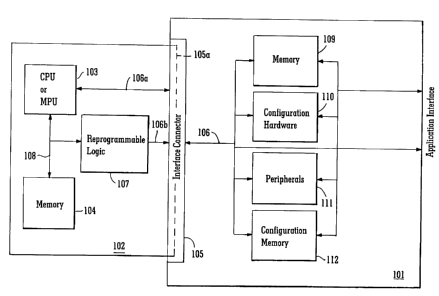
Figure 1 illustrates an embodiment of the invention wherein there is provided
a
daughtercard 102, including a central processing unit CPU) or micro processor
unit (MPU) 103, memory 104 and reprogrammable logic 107, connected to a
connector 105 on an application motherboard 101 by an edge connector 105a.
Other types of connections could also be used. The application motherboard
includes substantially all necessary functions for a particular application,
except for
the central processing sub-system functions. The central processing sub-system
functions required by a particular application are supplied by plugging in the
CPU-
based daughtercard 102. The interconnection between the CPU-based
daughtercard 102 and the motherboard lUl is now described in greater detail.
The CPU-based daughtercard 102 communicates with other components of the
application motherboard 101 via signals sent over a plurality of input/output
lines
106, 106a and 106b. However, as noted above, different CPUs are defined to
have
one or more different input/output lines and electrical characteristics.
Therefore,
at least some of the connections between the CPU 103 input/output lines and
the
motherboard are programmable (i.e. input/output lines 106b). In the
illustrated
embodiment, the CPU-based daughtercard input/output lines are connected to the
motherboard through an interface including edge connector 105a on the
daughterboard and socket connector 105 on the motherboard. Although in
conventional interconnect systems the individual conductors of such connectors
would be defined to correspond to specific functions of the CPU-based
daughtercard
input/output lines 106a and 106b, in this embodiment of the invention the CPU-
based daughtercard may be associated with the conductors and connectors
associated with input/output lines 106b in any convenient fashion. Thus, if
the
CA 02392503 2002-05-27
WO 0113899? PCT1GB99103946
9
CPU sub-system connections 108 have different physical and electrical
properties
they may be routed to any conductors of the connector 105 on the daughtercard.
Conversely, if an alternative motherboard with different connections of
input/output lines on connector 105, the daughtercard may be routed to
different
conductors of the connector 105.
In this embodiment of the invention some of the CPU-based daughtercard
input/output lines 106b are mapped on to an electronic switching device such
as a
field-programmable gate array (FPGA) 107. An FPGA is one type of programmable
logic circuit device including a collection of general logic devices which may
be
connected together to form a desired logic function by programming.
Programming
usually involves loading a map of interconnections between the general logic
devices
into the FPGA. The general logic devices are usually serial logic elements,
such as
gates, but also include parallel and clock elements in many versions. The
logic
function embodied in a programmed FPGA may be as simple as a routing of
signals,
such as might be performed by a switch. However, the logic function may
include
such processing of signals as changing timing or polarity or function, may
produce
output signals not found among the input signals, or may include complete
functional blocks such as universal Asynchronous Receive/Transmitters (DARTS)
or Direct memory Access Controllers (DMACs). In use in embodiments of the
present invention, the FPGA may be programmed, but not limited to, any or alI
of
the tasks noted above.
On being programmed, the FPGA 107 performs the overall logic function
necessary
to map the collection of functions required by the CPU sub-system connections
108
CA 02392503 2002-05-27
WO 01138997 PCT/GB99l03946
to the input/output lines 106b of the daughtercard connector 105. For example,
a
particular CPU 103 may issue memory read and write requests using one set of
signals transmitted over the CPU sub-system connections 108, whereas the
motherboard connections 106 may include a different set of signals to perform
read
and write functions in an attached memory 109. The FPGA logic function is thus
designed to map between the two distinct representations of a similar
function.
Further, the CPU-based daughtercard FPGA Iogic function may configure the
input/output lines to conform to standard bus configurations, such as ISA or
PCI,
bespoke bus configurations such as CPU native, or application motherboard
custom connections such as peripherals 111, and include connections to
functional
blocks within the FPGA.
The motherboard 101 in this embodiment contains additional program memory 109
containing application program information specific to an individual
motherboard
that can be executed by the CPU or MPU I03 on the daughtercard 102.
The motherboard also contains configuration hardware 110 such as switches,
jumpers and resistors that can be read by the daughtercard and allow the
daugk~tercard to configure itself according to the configuration hardware
information. The motherboard also contains configuration memory 1 12 that can
be
read by the daughtercard, and which allows the daughtercard to configure
itself
according to the configuration memory information.
A person or ordinary skill in this art is capable of designing such a mapping
given
the various signal functions and timing requirements. It should also be
evident
that although this embodiment employs an FPGA, any similar programmable logic
CA 02392503 2002-05-27
WO 01/38997 PCT1GB99I03946
11
circuit may be used, without regard to whether that circuit resides in a
single
package or multiple packages.
Figures 2 and 3 show the read-only memory (ROM) 104 and its contents on the
CPU-based daughtercard 102. One purpose for this ROM I04 is to hold the
program for the FPGA 107. Each CPU 103 is accompanied by a ROM 104
containing a program which properly maps the CPU sub-system connections 108
for the CPU 103 to the application motherboard connector 105 and the
motherboard connections 106. Thus in the case of the illustrated embodiment of
the invention, when the CPU-based daughtercard 102 including the CPU 103 is
plugged into the motherboard 101, the FPGA 107 may be loaded via the CPU sub-
system connections 108 with different programs corresponding to the mapping
required for different CPUs 103 and motherboards 101.
Figure 3 shows an example memory map for the daughtercard 102. The programs
and data of Figure 3 are stored in memory 104 of the daughtercard. When the
daughtercard starts executing a program in the ROM 104, it first accesses a
Reprogrammable Logic Loader Program 201 which tells the CPU or MPU 103 to
program the reprogrammable logic 107 with the information stored in a
Reprogrammable Logic Application Interface Image 203 area of memory. When this
is completed, the CPU executes the program /and uses data) from the
Application
Program and Data area 202 of the memory.
The memory 104 provided on the CPU-based daughtercard 102 need not be strictly
read-only but should include a non-volatile memory type, Any suitable type of
memory which retains its contents while power is not applied to the
daughtercard
CA 02392503 2002-05-27
WO 01138997 PCT/GB99/03946
12
102 may be employed. Thus, although the program for the FPGA 107 is retained
during intervals of power being off, the CPU-based daughtercard 102 could be
reprogrammed, when improvements are made to the FPGA program corresponding
to the CPU 103 or the application motherboard 101 or a new application or
motherboard is produced. Electrically alterable read-only (EAROM) is an
example
of a memory which is non-volatile and hence, used primarily in a read-only
mode,
but whose contents may be changed from time to time as required.
Furthermore, holding the program for FPGA 107 need not be the only function of
a
ROM or similar memory 104 on the CPU-based daughtercard 102. For example,
the ROM 104 may include instructions for programming other devices, additional
configuration data for use by the CPU 103, or program instructions far one or
more
CPU functions. Other applications of that space in the ROM 104 which is not
used
by the FPGA program will become apparent to those designing specific
applications.
The FPGA 107 may be loaded with the configuration program contained in the ROM
104 upon the occurrence of any convenient event. For example, the FPGA 107 may
be loaded at system power up, or upon issuance of a reset signal as a result
of
operator intervention. Other automatic and operator intervention events which
may
be used at appropriate times to load or partially reload the FPGA 107 will be
readily
apparent to those skilled in the art who may be developing any particular
application.
It will be readily apparent to those skilled in this art that the invention
may be
practised using technologies other than the conventional printed wiring
technology
involving conventional motherboards and daughtercards in connection with which
CA 02392503 2002-05-27
wo om~~ rcr~cBmoa~~
13
the invention has been illustrated. For example, the circuitry described above
as
being associated with a daughtercard may be included in some type of hybrid or
other integrated module, including integration onto a single component. The
FPGA
107 and connector 105 technologies may be similarly varied, in accordance with
generally accepted design techniques. For example, the connectors 105 may
simply
be a socket into which all hybrid CPU sub-system modules 102 may be designed
to
fit. Therefore, it is intended that the terms motherboard 101, daughtercard
102
and related terms in this application be broadly construed to include any
technology by which the separation of function and connections between those
functions discussed above may be accomplished.
Figures 4 and 5 show a further daughterboard. Read-only memory 104 rnay, for
example, contain more than one FPGA map, and configuration hardware 110
included on the motherboard show the identification of the type of motherboard
101. This may for example, take the form of switches or wire jumpers or the
like, or
a memory containing configuration data. The CPU would read this motherboard
configuration hardware 110. Upon receipt of a motherboard identification from
configuration hardware 110, the CPU-based daughtercard would then correctly
and
appropriately self configure the programmable logic circuits 107. If no
correct
identification was found, the CPU-based daughtercard could put itself into a
safe
state.
Figure 5 shows an example memory map for the daughtercard 102 of Figure 4
which would configure itself based on configuration information from the
motherboard 10I (Figure 1). When the daughtercard starts executing a
Reprogrammable Logic Configuration Checker Program 301 in the ROM, it first
CA 02392503 2002-05-27
WO 01!38997 PCT/CB99l03946
14
accesses the motherboard to read the configuration information in the
configuration
hardware 110 (Figure 1). On the basis of this information the Reprogrammable
Logic Loader Program 301 tells the CPU or MPU 103 to program the
reprogrammable logic with the correct Reprogrammable Logic Application
Interface
Image 303, 304, 305 appropriate to the configuration hardware found on the
motherboard. When this is completed, the CPU exer_utes the program (and uses
data) from the Application Program and Data area 302 of the memory. This
example shows 3 configurations stored, but this could be any number
appropriate
to the number of motherboard configurations required.
Figures 6 and 7 show a further variant of the daughtercard 102. Read-only
memory 112, may for example, be on the motherboard. This memory contains
Reprogrammable Logic Application Interface Image 401 to be used by the
daughtercard 102. The daughtercard Reprogrammable Logic block 107 (suitably an
FPGA} reads this memory and then self configures the programmable logic
circuits.
Alternatively, the CPU-based daughtercard 102 could retrieve a new
Reprogrammable logic Application Interface Image 401 for the FPGA and store
this
in its own memory 104. The motherboard Configuration memory may contain other
information 402 that is needed by the motherboard and daughtercard such as a
program or data information.