Note: Descriptions are shown in the official language in which they were submitted.
CA 02392714 2002-05-27
WO 01/40839 PCT/US00/10243
OPTICAL FIBER CONNECTOR SYSTEMS
BACKGROUND OF THE INVENTION
The present invention relates to an optical fiber
connector system. More particularly, the present invention
relates to a connector assembly for optically coupling a
circuit card to a backplane.
The use of optical fibers for high-volume high-speed
communication is well established. As the volume of
l0 transmitted information grows, the use of optical fiber
cables including multiple optical fibers, and of systems
using multiple optical fiber cables, has increased.
It has long been desirable to increase the number of
fibers that can be removably connected within a given space.
Until recently fiber optic interconnects were limited to
single or duplex formats utilizing industry standard
connectors, such as the SC, ST, LC, and the like. These
solutions are analogous to single end electrical cable
terminations prevalent prior to the invention of electrical
ribbon cable and mass-terminable IDC connectors.
Fiber optic terminations currently are evolving from
single terminations to mass terminations. Within the past
few years, ribbonized multi fiber cables have been
developed. In conjunction with these cable development
efforts, multi-fiber mounting ferrules also have been
developed.
The design of traditional electronic cabinets is now
being utilized to accommodate optical and opto-electronic
devices. In traditional cabinet designs, the cabinet
comprises a box having a plurality of internal slots or
racks, generally parallel to each other. Components are
mounted on planar substrates, called as circuit boards or
daughter cards, which are designed to slide into the slots
or racks within the cabinet.
CA 02392714 2002-05-27
WO 01/40839 PCT/US00/10243
As with electrical cables, the need exists to provide a
means to allow the fiber signals to be passed through the
backplane of electronic cabinets. A backplane derives its
name from the back (distal) plane in a parallelepipedal
cabinet and generally is orthogonal to the board cards. The
term backplane in the present invention refers to an
interconnection plane where a multiplicity of
interconnections may be made, such as with a common bus or
other external devices. For explanation purposes, a
backplane is described as having a front or interior face
and a back or exterior face.
An example of a backplane connectivity application is
the interconnection of telephone switching equipment. In
this application, cards having optical and electronic
telecommunication components are slid into cabinets. The
need exists to have a removable fiber termination from both
the front side and the back-side of the backplane.
Furthermore, as a function of inserting and removing an
optical driver card from a rack coupled to the backplane,
coupling and uncoupling of the optical connections in the
card is to be completed in a blind mating manner.
In order to maintain appropriate transmission of light
signals, optical fiber ends are to be carefully aligned
along all three movement (x, y, and z) axes, as well as
angularly. Alignment challenges increase and tolerances
decrease geometrically as the number of optical fibers to be
aligned increases. Blind mating of a card-mounted component
to a backplane connector has been found to create special
challenges with regards to alignment and mating force issues
along the axis of interconnection.
For the purposes of the present description, the axis
of interconnection is called the longitudinal or x-axis and
is defined by the longitudinal alignment of the optical
fibers at the point of connection. Generally, in backplane
2
CA 02392714 2002-05-27
WO 01/40839 PCT/US00/10243
applications, the longitudinal axis is collinear with the
axis of movement of the cards and the axis of connection of
the optical fibers in and out of the cabinets. The lateral
or y-axis is defined by the perpendicular to the x-axis and
the planar surface of the card. Finally, the transverse or
z-axis is defined by the orthogonal to the x-axis and the
backplane surface. The angular alignment is defined as the
angular orientation of the card with respect to the x-axis.
In preferred embodiments, the motion of sliding the
card into a receiving slot simultaneously achieves optical
interconnection. The "optical gap" distance along the
longitudinal axis between the optical fiber ends and
interconnected optical components is an important
consideration. A large gap will prevent effective
connection, thereby causing the loss of the optical signals.
On the other hand, excessive pressure on the mating faces,
such as that caused by "jamming in" a card, may result in
damage to the fragile optical fiber ends and mating
components. Traditional optical gap tolerances are in the
order of less than one micron.
Current connector assemblies include forward biased
spring mounted ferrules. The purpose of the said bias
springs is twofold, one, to absorb a limited amount of over
travel of the ferrules during mating and two, to provide a
predetermined spring biasing force thus urging the ferrules
intimately together when the ferrules are in their mated
position.
An additional subject of concern is card gap,
especially when dealing with backplane connector systems.
Card gap is defined as the space remaining between the rear
edge of a circuit card and the interior or front face of the
backplane. In general, designers and users of backplane
connection systems find it exceedingly difficult to control
the position of a circuit card to a backplane within the
3
CA 02392714 2002-05-27
WO 01/40839 PCT/US00/10243
precision range required for optical interconnects. Card
gap, otherwise defined as card insertion distance, is
subject to a multiplicity of variables. Among these
variables are card length, component position on the surface
of the card, card latch tolerances, and component position
on the backplane.
Over insertion of a circuit card relative to the
interior surface of a backplane presents a separate set of
conditions wherein the backplane connector's components are
subjected to excessive compressive stress when fixed in a
mated condition. In certain instances the said compressive
stress may be sufficient to cause physical damage to the
connector's components and the optical fibers contained
therein.
The need remains for a connector system that prevents
component damage due to excessive operator force,
compensates for longitudinal card misalignment, yet provides
accurate control of optical gap distance and mating force.
Another consideration is radial misalignment of the
card. When an operator inserts a card on a slot, it is
often difficult to maintain the card edge perfectly aligned
in parallel with the lateral axis of the backplane. Figure
1 illustrates an angularity misaligned card 10 having a
connector 12 mating to a backplane connector 14. The card
is otherwise correctly aligned along the y and z-axes. At
the point of contact between connectors 12 and 14, the
angular misalignment prevents correct gap spacing between
optical fibers 16 and causes undue pressure on one end of
the connector and the respective optical fiber end faces.
Other considerations exist in backplane interconnection
systems other than correct alignment. With the advent of
laser optical signals and other high-intensity light
sources, eye safety is a major concern associated with
backplane connector users today. The safety issues are
4
CA 02392714 2002-05-27
WO 01/40839 PCT/US00/10243
further escalated by the fact that ribbonized fiber arrays
present a greater danger than the single fiber predecessors
because the amount of light is multiplied by the number of
fibers.
Previous systems, such as that discussed in U.S. Patent
No. 5,080,461, discuss the use of complex door systems
mounted on terminating fiber connectors, but mainly for the
purpose of preventing damage or contamination of fiber ends.
As the light-transmitting core of a single mode fiber
measures only ~ 8 microns in diameter, even a minute
accumulation of dust particles may render the fiber
inoperable. However, prior systems require complex
terminations at each fiber end and only may be mated to
another corresponding male-female connector pair, not to
standard connectors, making their use cumbersome.
EMI (electro-magnetic interference) control also has
arisen as an issue in backplane connector design. As
connection of optoelectronic devices through a backplane
often necessitates forming of a physical opening through the
backplane of an electronic cabinet, the potential exists for
EMI leakage through the said backplane. Electrical
interconnection has attempted to address this problem
through the use of several elaborate EMI shielding
techniques. However, current optical fiber connectors have
failed to satisfy this concern.
Finally, another concern regarding backplane optical
connector applications is bend radius control. Horizontal
cabinets connections are often subject to bend stresses due
to gravity, operator misuse, or physical constraints, such
as when a cabinet is pressed against a wall. Optical fibers
are made of glass and rely on total internal reflection to
transmit light signals. When an optical fiber is bent
beyond a certain critical angle, fractures may appear in the
glass, causing the fiber to break or become damaged. Also,
5
CA 02392714 2002-05-27
WO 01/40839 PCT/US00/10243
at certain bend angles, even if the glass fiber does not
break, the optical signal may be lost or may deteriorate, as
the complete light signal is no longer contained inside the
fiber.
Several methods and apparatus for controlling the bend
radius of an optical cable have been attempted. Among those
are pre-formed boots that are slid over the cable, external
devices such as clips or clamps, and elaborate injection
molded components that are shaped such that when attached to
l0 a cable, the cable assumes the shape of the molded
structure.
Since backplane connection frequently involves
connecting an increasing number of optical fibers in a small
space, the need exists for an apparatus for controlling the
bend radius of the optical fibers.
SUMMARY OF THE INVENTION
The present invention relates to an optical fiber
interconnect system that provides longitudinal and angular
alignment control, contamination control, visual safety and
bend radius control. In certain embodiments, the optical
interconnect system of the present invention provides for
interconnecting arrays of optical fiber cables in a
individual or collective fashion.
The fiber optic connector system of the present
invention is designed for connecting at least one optical
fiber cable mounted near the edge of a planar substrate, a
card, through a backplane. Each optical fiber cable
includes a plurality of optical fibers and a terminating
ferrule, the longitudinal orientation of the optical fibers
within the terminating ferrule defining a longitudinal axis
and a forward direction towards the backplane. Each optical
6
CA 02392714 2002-05-27
WO 01/40839 PCT/US00/10243
fiber cable is terminated by a ferrule having a first
longitudinal range of motion x1 with respect to a retaining
member and a ferrule spring element having a longitudinal
ferrule spring force fn.
The optical connector system comprises a card housing
assembly and a backplane housing assembly. The card housing
assembly is mounted on the planar substrate or card and
includes at least one ferrule-receiving cavity for receiving
the optical fiber ferrule. The card housing assembly
includes a card housing spring. The card housing assembly
has a longitudinal range of motion x2 with respect to the
card, the card housing assembly spring controlling movement
of the card housing assembly along the longitudinal range of
motion. The card spring has a longitudinally directed
spring force h, wherein
h>~"
that is, the spring force of the card spring can
counteract the opposite spring force of all the ferrule
springs. It should be understood that the ferrule spring
may comprise one or more individual spring elements. In one
embodiment of the present invention, the card spring
includes two or more springs laterally spaced from in each
other, to create an independent card suspension that
compensates for angular misalignment along the x-y plane.
The backplane member has a first surface and a second
surface. The backplane housing include at least one
longitudinal receiving cavity, matching a respective cavity
in the card housing assembly. The receiving cavity has a
frontal opening along the first surface of the backplane
member and a rear opening along the second surface of the
backplane member. A frontal door covers the frontal opening
and a rear door covers the rear opening. In a particular
embodiment, the doors are spring elements made of a
flexible, conductive material and biased towards a closed
7
CA 02392714 2002-05-27
WO 01/40839 PCT/US00/10243
position. To provide EMI protection, the doors may be
electrically connected to ground. In another particular
embodiment, the backplane housing comprises two members, one
coupling to the first side of the backplane and the second
coupling to the second side of the backplane. To provide
EMI protection, one of the members may include an
electrically conductive material electrically connected to
ground.
The interconnect system also may include one or more
optical cables including a bend radius control member for
controlling the bend radius of an optical fiber cable. The
bend radius control member comprises a deformation resistant
heat-shrinked outer jacket wrapped around the optical fiber
cable, wherein the heat-shrunk outer jacket has a desired
bend radius curvature.
BRIEF DESCRIPTION OF THE DRAWINGS
Figure 1 is a side elevation view of an angularly
misaligned card and a backplane connector.
Figure 2 is an isometric cut-away view of a first
embodiment of a connector system in accordance with the
present invention in a coupled card position.
Figure 3 is an isometric view of the connector system
illustrated in Fig. 2 in an uncoupled card position.
Figure 4 is an exploded isometric view of the connector
system illustrated in Fig. 2.
Figure 5 is an isometric cut-away view of the backplane
housing assembly of the connector system illustrated in Fig.
2.
Figure 6 is an isometric view of the card housing
assembly of the connector system illustrated in Fig. 2.
8
CA 02392714 2002-05-27
WO 01/40839 PCT/US00/10243
Figure 7 is an isometric view of the card-facing face
of the housing assembly of the connector system illustrated
in Fig. 2.
Figure 8 is a side elevation view of a backplane
connection system wherein the connector components are
aligned along the axis of the interconnection even though
the circuit card is angular with respect to the said axis of
interconnection.
Figure 9 is an isometric view of the plug portion of
the connection system illustrated in Fig. 4.
Figure 10 is an isometric exploded view of plug
illustrated in Fig. 4 showing the plug fully assembled
except for the installation of the cover.
Figure 11 is an isometric view of the plug illustrated
in Fig. 4 with its cover being installed.
Figure 12 is an isometric view of the plug illustrated
in Fig. 4 fully assembled.
Figure 13 is an isometric view of the plug assembly
illustrated in Fig. 11 wrapped about a forming fixture.
DETAILED DESCRIPTION OF THE INVENTION
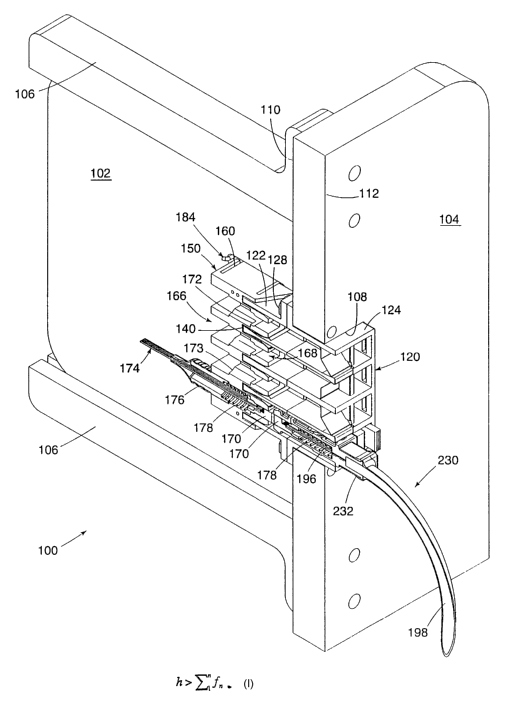
Figures 2 and 3 illustrate an embodiment of an optical
interconnect system 100 in accordance with the present
invention. The optical interconnect system 100 couples a
circuit card or daughter card 102 with and through a
backplane 104. The card 102 is a planar substrate, such as
a circuit card or daughterboard, which may include optical,
optoelectronic, and electronic components. The card 102 may
be slideably inserted in a slot defined by card guides 106.
The backplane 104 includes a through opening 108, a first
interior surface 110 and a second, exterior surface 112.
9
CA 02392714 2002-05-27
WO 01/40839 PCT/US00/10243
The optical interconnect system 100 includes a
backplane housing 120 disposed within opening 108. The
backplane housing 120 includes, in the present embodiment, a
first portion 122 and a second portion 124. The first
portion 122 includes male locating features 126 that engage
with corresponding female features (not shown) on a rear
face of the second portion 124. Locating features three
help ensure accurate alignment between the backplane housing
portions 122 and 124 during assembly. It should be
understood that in alternative embodiments housing portions
122 and 124 do not need to be separate and could be molded
as one piece. Splitting off the housing portions 122 and
124, however, may allow for more freedom in mold core
design.
In the present embodiment, fasteners 128 secure the
backplane housing assembly 120 to the backplane 104.
Fasteners 128 include threaded metal inserts inserted
through matching bores 130 in the first and second portion
122 and 124 of the backplane housing 120. Those skilled in
the art will readily appreciate that mounting screws are
used in conjunction with fasteners 128 and that a variety of
fastening mechanisms, adhesives, interference fitting, and
other devices known in the art may be used to align and
secure the backplane housing assembly 120.
The backplane housing assembly 120 defines an array of
four receiving cavities 132. Alternative embodiments may
include a single receiving cavity or any other necessary
number of cavities to accommodate various optical fiber
cable connections. Each one of the cavities 132 includes a
front opening 134 and a rear opening 136. For the purpose
of the description of the present invention the terms rear,
front, forward or backward are merely illustrative to help
describe the depicted embodiments with respect to the
figures. The folding front doors 138 are coupled to close
CA 02392714 2002-05-27
WO 01/40839 PCT/LTS00/10243
the front opening 134 and rear doors 140 are coupled to
close rear openings 136. The front and rear doors 138 and
140 in the present embodiment include flat spring metal
members hingedly coupled to the front and rear openings 134
and 136. The doors 138 and 140 are designed to fold down
flat when a plug is inserted into the opening of the
receiving cavity 132. In the present embodiment, the
backplane housing assembly 120 comprises molded plastic
pieces of a dielectric material that exhibit the structural
l0 strength and dimensional stability required to maintain
control of the optical fiber's position. Such materials
include, but are not limited to, thermoplastic injection
moldable polymers that are filled or unfilled with
reinforcement agents, and transfer moldable polymers such as
epoxy. The doors 138 and 140 are made of a conductive metal
material, such as tempered stainless steel, beryllium/copper
alloys or other materials, and are coupled to provide a
grounding electrical path. The doors 138 and 140 provide
three functions:
1) to provide a physical barrier to limit ambient
contamination from entering the assembled
connector housing,
2.) to absorb and route to ground electric magnetic
interference that may otherwise leak through the
cavities 132 through the backplane 104; and
3) to provide eye safety from emitted light signals
from either end of the backplane.
The backplane housing assembly 120 may include mating
features corresponding to common plugs or ferrules. The
dual door design allows for the sealing of the optical
connection without the need to include special gated
terminations at each connector. The double door arrangement
also allows for at least one door to be closed any time a
receiving cavity is not filled by both a rear and a front
11
CA 02392714 2002-05-27
WO 01/40839 PCT/US00/10243
plug. Finally, the use of conductive metal doors retained
in a conductive housing assembly 24 allows for the
containment and grounding of EMI components, using a
relatively simple and elegant design. In embodiments where
the user is not concerned with any of the above issues, the
use of doors may be optional without effecting the
performance and function of the backplane housing assembly
120.
Another useful feature of the housing assembly 120 is
l0 the use of side latch receiving features 142. While
traditional plug retaining features, such as that in a
conventional phone plug, are placed on top of a connector
plug and receiving housing, it was found that such an
arrangement unnecessarily interfered with the stacking of
ribbon flat optical fiber cables. The present invention
addresses this problem by placing the latch receiving
features along the same plane defined by the optical fiber
array in an optical fiber ribbon cable. This allows for
vertical stacking of a number of flat ribbon cables in a
reduced space.
The front end of the backplane housing assembly 120
mates with a board housing assembly 150 when the card 102 is
slid into the guide slots 106. The board housing assembly
includes a housing member 152, including hollow protrusions
154 shaped in size to correspond and fit into front openings
134 of the backplane housing assembly 120. The board
housing assembly 150 includes board attachment features 156
having a barbed end 158. The board attachment features 156
are designed to be inserted through a receiving slot 160 in
the planar substrate 102. While the board attachment
features 156 secures the board housing assembly to the board
in the transverse and lateral direction, a range of freedom
of movement along the longitudinal axis is allowed. The
present embodiment, the length of the slot 160 exceeds the
12
CA 02392714 2002-05-27
WO 01/40839 PCT/LJS00/10243
width of the alignment feature 156. Those skilled in the
art will be readily aware of additional methods for
attaching the board housing assembly 150 to the planar
substrate 102, while allowing freedom of movement in the x
direction. Alternative embodiments may include attachment
means such as mechanical fasteners, spring clips or the
like.
The protrusions 154 in the present embodiment are
hollow and rectangular shaped and are terminated in a
truncated pyramid shaped lead 162. The pyramid shaped lead
162 allow for compensation of certain mating misalignments
by directing the board housing assembly protrusions 154 into
the receiving cavities 132 of the backplane housing
assembly. Furthermore, the protrusions 154 are shaped to
provide alignment with respect to the inside walls of
receiving cavities 132. Protrusions 154 also provide an
automatic pressure for opening front doors 138 during
mating. The inner walls of protrusion 154 define a stepped
cavity 164 that provides guidance to a fiber optic ferrule
170 to be seated inside of the stepped cavity 164. The
present embodiment, the stepped cavity 164, is shaped to
receive an industry standard ferrule, such as the MT-Style
optical ferrules. Step cavity 164 is designed in such a
manner that it comprises a front and a rear rectangular
opening 166 and 168, respectively. The front opening 166 is
sized to allow insertion of the ferrule 170 up to an
internal flange 172. A typical MT-style connector includes
a ferrule 170 mounted on a stalk of optical fibers 174,
slidably connected to a detente body portion 176. The
ferrule 170 has a limited range of motion x1 along the
longitudinal axis. The stalk of optical fibers 174 is
allowed to move with respect to the detente body portion
176. A spring element located between the ferrule and the
13
CA 02392714 2002-05-27
WO 01/40839 PCT/US00/10243
detente body portion forward biases the ferrule towards a
forward end of the range of motion.
In the present embodiment, the board housing assembly
150 includes rear openings 168 designed to accept the MT
connector, including the detente body portion 176. The
detente body portion 176 is retained against flange 173
while the ferrule 170 is allowed to extend inside of
protrusion 154 up to and through the rear opening 168. The
detente member 176 is designed in such a manner that as the
l0 member 176 is inserted into the front of the stepped cavity
164, the spring 178 is compressed between detente member 176
and the ferrule 170. The ferrule 170 is prevented from
travelling freely through the rear opening 168 by a flange
180 formed in the ferrule 170. The flange 180 is formed to
act as a travel stop for the ferrule 170 when flange 180 is
engaged with internal flange 172. The detente member 176 is
provided with a latch feature that engages the rear opening
168 of the board housing assembly 150. Preferably, latching
features are provided on both side surfaces of the housing
assembly 150 and the detente member 176. It may be
desirable in some instances to remove detente member 176
from the housing assembly, and for these situations, a
release feature is provided in the side of the housing.
This release feature is cantilevered and allowed to pivot
and thereby allowing the release feature to be sprung
outwards to release the corresponding latch feature.
The length of travel of the card 102 along the card
guides 106 is selected such that when in the coupled
position the board housing assembly 150 exerts spring force
on the backplane housing assembly 120. In a preferred
embodiment, the width of the card gap should be greater than
0, preferably greater than the combined travel of the spring
biased ferrules (typically 1 to 2 mm) relative to their
respective housings.
14
CA 02392714 2002-05-27
WO 01/40839 PCT/US00/10243
The range of motion x2 of the board housing assembly 150
with respect to the card 102 is sufficient to correct for
tolerance errors in the range of movement of the card 102
along the card guides 106, and to absorb any excessive force
imparted by the user when sliding the card before the card
is stopped by the backplane housing 120 or by the stop
features if present in the card guides 106. The present
invention addresses issues or overcompression by allowing
the circuit card's attached connector components to move
relative to the said circuit card. Accordingly, in the
coupled position, the board housing assembly 150 is held
tightly against the back of the backplane housing assembly
120 and is subject to a constant spring bias provided by
spring assembly 184. The advantage of providing the
constant spring bias is to ensure that intimate contact is
maintained between the housing assemblies 150 and 120 even
in the event that the card 102 is subject to movement during
its operation.
Figure 5 illustrates a detailed cutaway view of
backplane housing assembly 120 having front and rear doors
138 and 140. The doors 138 are designed such that when the
protrusions 154 of board housing assembly 150 are inserted
into the front opening 134, the pyramid shaped lead 162 of
the protrusions 154 forces the front door 138 to fold down.
Similarly, when a plug 190 is inserted into rear opening
136, the insertion of the plug 190 causes rear door 140 to
fold down. Doors 138 and 140 are preferably formed of a
spring-like material that withstands numerous cycles of
being folded to an open position and then returning to a
closed position when the plug 190 or protrusion 154 is
removed. In instances where EMI protection is a concern,
the rear doors 140 and the first portion 124 of the
backplane housing may be constructed of a conductive
material such as metal. When made of a conductive material,
CA 02392714 2002-05-27
WO 01/40839 PCT/US00/10243
the rear door 140 and the first portion 124 will absorb the
majority of any EMI radiation that would otherwise escape
through the cavities 132. The first portion 124 is then
electrically coupled to a ground end feature. In
alternative embodiment, either the doors 140 or the first
portion of the backplane housing 122 may be constructed of a
dielectric material, leaving only one conductive element.
The remaining conductive portion would then be coupled to
ground.
l0 By providing both a front door 138 and a rear door 140
covering both the front opening 134 and the rear opening
136, the removal of either plug 190 or the card housing
assembly 150 results in the closing of one of the doors,
thus alleviating any possible visual safety risk. It should
be understood that each door is allowed to function
independently of the other. Accordingly, that means that if
only one plug 190 is inserted into the rear opening 136, the
rear doors 140 of the remaining receiving cavities 132 will
remain closed. To further assure the tight fit of the doors
138 and 140 within the openings 134 and 136, frame features
144 may be formed on the side walls of the receiving
cavities 132 that match the side profile and overlap the
side edges of doors 138 and 140. This further creates a
tighter seal to prevent contamination, contain EMI, and
prevent light leakage.
Figures 6 and 7 illustrate the positioning of springs
184 inserted into spring receiving openings 186 and housing
assembly 150. Springs 184 are wire springs having a wire
diameter sized such that the wire springs 184 provide a
slight pressed fit between the spring, board attachment
features 156 and the receiving boards slots 160. With
springs 184 inserted into the spring receiving openings 186,
the board attachment features 156 are prevented from
flexing, thereby locking the housing assembly 150 to the
16
CA 02392714 2002-05-27
WO 01/40839 PCT/US00/10243
card 102. Referring in particular to Figure 6, one may
appreciate how slots 160 provide passage through card 102
for the board attachment features 156. The barbed end 158
of the board attachment features 156 is designed as to grip
the back side of card 102 thereby securing the housing
assembly 150 along the transversed axis to the daughtercard
102. The slots 160 are sized such that the board housing
assembly 150 has a range of movement x2 along the
longitudinal axis on the surface of the card 102. The
combination of the forward bias of the spring assembly 182
and the freedom of movement x2 of the housing assembly 150
allows to compensate for incorrect tolerances in the
alignment of the card 102 with respect to the backplane 104.
The combined force of the springs 184 of spring assembly 182
IS is selected to be greater than the summation of all opposing
spring forces such as those of the independent springs 178
of the individual ferrule assemblies. Otherwise, the
combined force of the springs 178 of the ferrule assemblies
would push the housing assembly backwards thus preventing
the desired coupling between the board housing assembly 150
and the backplane housing assembly 120. However, as the
forward movement of the board housing assembly 150 will be
limited by flange 151, the independent ferrules still retain
their range of movement, thus assuring a tight fit on each
individual optical cable connection.
As illustrated in Figures 6 and 7 the longitudinal
movement of the board housing assembly 150 is controlled by
a spring assembly 182. The term spring refers to a
resilient or elastic member, such as a coiled spring, a
biasing clip, an elastic band, a compression foam, or other
similar devices known in the art. In the present
embodiment, the spring assembly 182 includes two spring
clips 184 laterally spaced with respect to each other and
located generally at the lateral ends of the board housing
17
CA 02392714 2002-05-27
WO 01/40839 PCT/US00/10243
assembly 150. The spring assembly 182 serves three
functions (a) to exert a forward force along the
longitudinal axis on the board housing asselmbly 150, thus
creating a spring bias between board housing assembly 150
and the board 102 that the board housing assembly 150 is
mounted on; and (b) to lock the board latching features 156,
thus preventing the board housing assembly 150 from
inadvertently being removed from the board; and (c) to
provide compensation for angular misalignment of the card.
The spring assembly 182 preferably biases the board
housing assembly 150 towards the front or mating edge of the
daughter card, such that the board housing assembly 150 is
forced to move against the resistance of springs 184 when
the board housing assembly 150 is moved by an action
opposite to that of the normal force of the springs 184.
Furthermore, as illustrated in Figure 8, the placement
of the two springs 184 at laterally spaced locations allows
for the correction of angular misalignments, thus reducing
the pressure and possible damage on the leading edge of the
backplane housing assembly 150 and compensating for angular
misalignment of the port.
Figures 9 -11 illustrate the plug assembly 190. The
plug assembly 190 is designed to receive a conventional MT-
style connector ferrule and provide connectorization
features to match the backplane housing assembly 120. Those
skilled in the art will readily appreciate that the plug
assembly may be molded to receive different types of
connectors. In alternative embodiments of the present
invention, the backplane housing assembly may be shaped to
receive directly traditional connector assemblies.
The plug assembly 190 is comprised of a lower housing
member 192 and housing cover 194. As explained above, a MT
style connector assembly includes a ferrule 170, and a
ferrule spring 178. The MT style connector is used to
18
CA 02392714 2002-05-27
WO 01/40839 PCT/US00/10243
terminate a multi-fiber ribbon cable 196 that is surrounded
by a protective jacket 198.
The lower housing component 192 includes a front
opening 200 defined by flange surfaces 202, a receiving well
204, and a spring-retaining lip 206. The ferrule 170 has a
front portion 171 and a flange 172. The front portion 171
passes through opening 200. However, opening 200 is sized
such that the flange 172 is too large to pass through
opening 200 and the flange 172 rests against the flange
surfaces 202. The end 179 of ferrule spring 178 when
positioned properly within lower housing 192, as seen in
Fig. 10, rests within receiving well 204 and is compressed
between flange 172 and the spring-retaining lip 206. The
compression of ferrule spring 178 results in a force being
exerted against flange 172 and lip 206, therein spring
biasing ferrule 170 forward through opening 200.
Fig. 11 illustrates housing cover 194 positioned for
attachment to lower housing 192. This attachment is
facilitated by placing engaging features 208 of housing
cover 194 into engaging cavity 210 present in the sidewalls
of the lower housing component 192. As housing cover 194 is
rotated in a downward direction, engagement features 208 are
trapped within engagement cavity 210. As the rotation
progresses male snap latches 212 are engaged with the
respective female latch receiving features 214, locking
lower housing component 192 and housing cover 194 together.
An opening 216 is provided in lower housing component
192 to provide a path for strength members 218 to pass
through. The strength members 218 are generally present in
fiber optic cables and are typically attached to the
housings of fiber optic connectors to relieve axial stress
on the cable's optical fibers.
The lower housing component 192 also includes cavities
220 into which posts 222 of the housing cover 194 are
19
CA 02392714 2002-05-27
WO 01/40839 PCT/US00/10243
inserted during the assembly procedure to provide lateral
locking and alignment of the housing cover 194 to the lower
housing component 192.
Fig. 12 illustrates plug assembly 190 assembled onto
the optical fiber cable 196 with a bend radius control
member 230 installed. The bend radius control member 230
for purposes of this illustration is comprised of a
shrinkable tubing that has been applied over a rear housing
section 232 of plug assembly 190, the cable's protective
l0 jacket 198, and the cable's strength members 218. The bend
radius control member 230 is heated and shrunk into position
therein securing cable 196 to the plug 190.
Fig. 13 shows a cable forming device 250 comprising a
vertical support 255 fastened to a base plate 254 and one or
more forming mandrels 256 that are attached to vertical
support 252. The radius of the mandrels 256 exceeds the
critical bend radius for the optical fiber cable 196. The
angles of the mandrels 256 with respect to each other
correspond to the expected or desired path for the optical
fibber cable 196.
To apply the bend radius control member 230, a
shrinkable tubing or jacket 262 is first slid or wrapped
over the plug assembly 190 and the optical fiber cable 196.
The term heat-shrinkable jacket or tubing is intended to
include tubing, jackets, tapes, wraps or coatings comprising
heat-shrinkable materials that may be wrapped around the
desired portion of the optical fiber cable. The term heat-
shrinkable jacket refers to a material that, when heated,
collapses and compresses around the optical fiber cable, and
remains in this collapsed shape upon returning to ambient
temperature, such as heat-shrinkable plastics.
The cable 196 and the shrinkable tubing 262 are wrapped
about mandrels 256. The illustrated device 250 produces a
dual bend wherein the cable 196 is formed down and left thus
CA 02392714 2002-05-27
WO 01/40839 PCT/US00/10243
creating a compound bend. The shrinkable tubing is then
heated to a temperature sufficient to cause the tubing to
shrink. In the present embodiment the heat exposure
required to collapse the heat-shrinkable material is
selected to avoid any detrimental effects to the optical
fiber cable, yet to be higher than the normal operating
range for the optical fiber cable. Heat sources may include
hot air guns, irradiating heat elements, heated mandrels or
other suitable heat sources. The heating may be done before
placing the optical cable 196 on the mandrels 256 or
afterwards. The shrinkable tubing 262 and the cable 196
remain wrapped about mandrels 256 while the tubing is
allowed to cool. Once cooled, the cable 196 will assume the
desired shape and bend radius . The stiffness of the formed
cable may be controlled by the thickness and the durometer
of the material from which the shrinkable tubing is formed.
In certain instances it may be desirable to coat the
inner surface of the shrinkable tubing with a heat activated
adhesive that forms a bond with the protective jacket of the
optical cable 196 and with the rear housing section 232.
The bend radius control member may be applied to any portion
of the cable where a bend is expected or desired. Field
applications may be performed using a wrapable shrink
material and a portable heat source, such as a heat air gun
or lamp.
It should be noted that this invention is not limited
to the use of shrinkable tubing to provide strain relief and
bend radius control; however the use of shrinkable tubing
offers an inexpensive solution to an otherwise costly
problem.
Those skilled in the art will appreciate that the
present invention may be used when coupling a variety of
optical devices and even non-optical devices that require
precise alignment. While the present invention has been
21
CA 02392714 2002-05-27
WO 01/40839 PCT/US00/10243
described with a reference to exemplary preferred
embodiments, the invention may be embodied in other specific
forms without departing from the spirit of the invention.
Accordingly, it should be understood that the embodiments
described and illustrated herein are only exemplary and
should not be considered as limiting the scope of the
present invention. Other variations and modifications may
be made in accordance with the spirit and scope of the
present invention.
22