Note: Descriptions are shown in the official language in which they were submitted.
CA 02393007 2009-09-02
WO 01/41219 1 PCT/US00132084-
MICRO-LED ARRAYS WITH ENHANCED LIGHT EXTRACTION
BACKGROUND OF THE INVENTION
Field of the Invention
This invention relates to light emitting diodes and more particularly
to new structures for enhancing their light extraction.
Description of the Related Art
Light emitting diodes (LEDs) are an important class of solid state
devices that convert electric energy to light and commonly comprise an
active layer of semiconductor material sandwiched between two oppositely
doped layers. When a bias is applied across the doped layers, holes and
electrons are injected into the active layer where they recombine to
generate light. The light generated by the active region emits in all
directions and light escapes the device through all exposed surfaces.
Packaging of the LED is commonly used to direct the escaping light into
a desired output emission profile.
As semiconductor materials have improved, the efficiency of
semiconductor devices has also improved. New LEDs are being made
from materials such as GaN, which provides efficient illumination in the
ultra-violet to amber spectrum. Many of the new LEDs are more efficient
CA 02393007 2002-05-29
WO 01/41219 2 PCT/US00/32084
at converting electrical energy to light compared to
conventional lights and they can be more reliable. As
LEDs improve, they are expected to replace conventional
lights in many applications such as traffic signals,
outaoor and indoor displays, automobile headlights and
taillights, conventional indoor lighting, etc.
However, the efficiency of conventional LEDs is
limited by their inability to emit all of the light that
is generated by their active layer. When an LED is
energized, light emitting from its active layer (in all
directions) reaches the emitting surfaces at many
different angles. Typical semiconductor materials have a
high index of refraction (n2.2-3.8) compared to ambient
air (n=l.0) or encapsulating epoxy (nzzl.5) . According tc
Snell' s law, light traveling from a region having a high
index of refraction to a region with a low index of
refraction that is within a certain critical angle
(relative to the surface normal direction) will cross to
the lower index region. Light that reaches the surface
beyond the critical angle will not cross but will
experience total internal reflection (TIR). In the case
of an LED, the TIR light can continue to be reflected
within the LED until it is absorbed, or it can escape out
surfaces other than the emission surface. Because of this
phenomenon, much of the light generated by conventional
LEDs does not emit, degrading efficiency.
One method of reducing the percentage of TIR light
is to create light scattering centers in the form of
random texturing on the surface. [Shnitzer, et al., "300
External Quantum Efficiency From Surface Textured, Thin
Film Light Emitting Diodes", Applied Physics Letters 63,
Page 2174-2176 (1993)]. The random texturing is
CA 02393007 2002-05-29
WO 01/41219 3 PCT/US00/32084
patterned into the surface by using sub micron diameter
polystyrene spheres on the LED surface as a mask during
reactive ion etching. The textured surface has features
on the order of the wavelength of light that refract and
reflect light in a manner not predicted by Snell's Law
due to random interference effects. This approach has
been shown to improve emission efficiency by 9 - 30%.
One disadvantage of surface texturing is that it can
prevent effective current spreading in LEDs which have
poor electrical conductivity for the textured electrode
layer, such as the case of p-type GaN. In smaller
devices or devices with good electrical conductivity,
current from the p and n-type layer contacts spreads
throughout the respective layers. With larger devices or
devices made from materials having poor electrical
conductivity, the current cannot spread from the contacts
throughout the layer. As a result, part of the active
layer does not experience the current and will not emit
light. To create uniform current injection across the
diode area, a spreading layer of conductive material is
deposited on its surface. However, this spreading layer
often needs to be optically transparent so that light can
transmit through the layer. When a random surface
structure is introduced on the LED surface, an
effectively thin and optically transparent current
spreader cannot easily be deposited.
Another method of increasing light extraction from
an LED is to include a periodic patterning in the
emitting surface or internal interfaces which redirects
the light from its internally trapped angle to defined
modes determined by the shape and period of the surface.
See U.S. Patent No. 5,779,924 to Krames et at. This
technique is a special case of a randomly textured
CA 02393007 2002-05-29
WO 01/41219 4 PCT/USOO/32084
surface in which the interference effect is no longer
random and the surface couples light into particular
modes or directions. One disadvantage of this approach is
tnat the structure can be difficult to manufacture
because the shape and pattern of the surface must be
uniform and very small, on the order of a single
wavelength of the LED's light. The pattern can also
present difficulties in depositing an optically
transparent current spreading layer as described above.
An increase in light extraction has also been
realized by shaping the LED's emitting surface into a
hemisphere with an emitting layer at the center. While
this structure increases the amount of emitted light, it s
fabrication is difficult. U.S. Patent No. 3, 954,534 tc
is Scifres and Burnham discloses a method of forming an
array of LEDs with a respective hemisphere above each of
the LEDs. The hemispheres are formed in a substrate and
a diode array grown over them. The diode and lens
structure is then etched away from the substrate. One
disadvantage of this method is that it is limited to
formation of the structures at the substrate interface,
and the lift off of the structure from the substrate
results in increased manufacturing costs. Also, each
hemisphere has an emitting layer directly above it, which
requires precise manufacturing.
U. S. Patent No. 5,793,062 discloses a structure for
enhancing light extraction from an LED by including
optically non-absorbing layers to redirect light away
from absorbing regions such as contacts and also redirect
light toward the LED's surface. One disadvantage of this
structure is that the non-absorbing layers require the
formation of undercut strait angle layers, which can be
difficult to manufacture in many material systems.
CA 02393007 2002-05-29
WO 01/41219 PCT/US00/32084
Another way to enhance light extraction is to couple
photons into surface plasmon modes within a thin fil m
metallic layer on the LED's emitting surface, which are
emitted back into radiated modes. [Knock et al., Applied
Phvsics Letter 57, pg. 2327 2329 (1990) ] (Please
provide title of article) . These structures rely on the
coupling of photons emitted from the semiconductor into
surface plasmons in the metallic layer, which are further
coupled into photons that are finally extracted. One
disadvantage of this device is that it is difficult to
manufacture because the periodic structure is a one-
dimensional ruled grating with shallow groove depths
(<0. 1 um) . Also, the overall external quantum
efficiencies are low (1.4-1.5%), likely due to
15 inefficiencies of photon to surface plasmon and surface
plasmon-to-ambient photon conversion mechanisms. This
structure also presents the same difficulties with a
current spreading layer, as described above.
Light extraction can also be improved by angling the
20 LED chip's side surfaces to create an inverted truncated
pyramid. The angled surfaces provide TIR light trapped in
the substrate material with an emitting surface within
the critical angle [Krames, et. al. Applied Physics
Letters 75 (1999)] (Please provide title of article)
25 Using this approach external quantum efficiency has been
shown to increase from 35% to 50% for the InGaAl P
material system. This approach works for devices in which
a significant amount of light is trapped in the
substrate. For the case of GaN on sapphire, much of the
30 light is trapped in the GaN film so that angling the LED
chip's side surfaces will not provide the desired
enhancement.
Still another approach for enhancing light
CA 02393007 2002-05-29
WO 01/41219 6 PCTIUSOO/32084
extractor: is photon recycling. (Shnitzer, et al.
`Ultrahigh spontaneous emission quantum efficiency, 99.7%
internally and 72% externally, from A1GaAs/GaAs/A1GaAs
double heterostructures', Applied Physics Letters 62,
Page 131-133 ;1993) j . This method relies on LEDs having a
hign efficiency active layer that readily convert s
electrons and holes to light and vice versa. TIR light
reflects off the LED's surface and strikes the active
layer, where the light is converted back to an electron-
hole pair. Because of the high efficiency of the active
layer, the electron-hole pair almost immediately
reconverts to light that is again emitted in random
direction. A percentage of this recycled light strikes
one of the LEDs emitting surfaces within the critical
angle and escapes. Light that is reflected back to the
active layer goes through the same process again.
However, this approach can only be used in LEDs made from
materials that have extremely low optical loss and cannot
be used in LEDs having an absorbing current spreading
layer on the surface.
SUMMARY OF THE INVENTION
The present invention provides a class of new LEDs
having interconnected arrays of micro-LEDs to provide
improved light extraction. Micro-LEDs have a smaller
active area, in the range of 1 to 2500 square microns,
but the size is not critical to the invention. An array
of micro-LEDs is any distribution of electrically
interconnected micro-LEDs. The arrays provide a large
surface area for light to escape each of the micro-LEDs,
thereby increasing the usable light from the LED. The new
LED can have many different geometries and because it is
formed by standard semiconductor process techniques, it
CA 02393007 2002-05-29
WO 01/41219 PCT/US00/32084
7
s ;~igr.ly manufacturable.
The new LED includes a conductive first spreade r
layer witr micro-LEDs disposed on one of its surfaces
Each micro-LED has a p-type layer, an n-type layer and an
active layer sandwiched between the p- and n-type layers .
E-,tner the p- or n-type layer is a top layer and the
other is the bottom layer. Current applied to the first
spreader layer spreads into each micro-LED's bottom
layer. A second spreader layer is included over the
micro-LEDs and current from said second spreader spread
into the top layer. When a bias is applied across the
first and second spreader layers the micro-LEDs emit-
light.
One embodiment of the second spreader is a
15 conductive interconnected grid-like structure having
conductive paths over the micro-LEDs, in contact with the
top laver of the micro-LEDs. An insulator layer i s
included over the array with the grid on the insulator
layer, thereby electrically isolating the first spreader
20 layer from the grid.
Alternatively, flip-chip bonding can be used to
interconnect the micro-LEDs. Using this method, a n
unconnected micro-LED array is first formed and then
bonded to an electrically conductive material to provide
25 the array interconnection. In a third embodiment, the
grid passes over the micro-LEDs and the p-type, active,
and n-type material is under the conductive paths of the
grid between the micro-LEDs to electrically isolate the
grid from the first spreader layer. This grid-like
30 structure can be designed so that emitted light interacts
with a sidewall after traveling a small distance.
The new LED can have LEEs disposed between the
micro-LEDs or formed on the side surfaces of the micro-
CA 02393007 2002-05-29
WO 01/41219 8 PCT/USOO/32084
LEDs, to further enhance light extraction. The LEEs act
to redirect or focus light that would otherwise be
trapped or absorbed through TIR in a standard LED
structure. Their shapes may be curved (convex or concave)
:r oiecewise linear with the shape of the structure
affecting the light extraction and final output direction
of light. LEEs that are placed between the micro-LEDs
interact with light escaping from the sides of the micro-
LEDs. This interaction helps prevent the light from
reflecting back into the LED to be absorbed, thereby
increasing the useful light out of the LED.
These and other further features and advantages o f
the invention will be apparent to those skilled in the
art from the following detailed description, taken
together with the accompanying drawings, in which:
BRIEF DESCRIPTION OF THE DRAWINGS
FIG. 1 is a plan view of a the new LED with a micro-
LED array having an interconnecting current spreading
grid on an electrically insulating laver;
FIG. 2 is a sectional view of the new LED shown in
FIG. 1 taken along section lines 2-2;
FIG. 3 is a sectional view of another embodiment of
the new LED with its micro-LED array bonded to a submount
using flip-chip mounting;
FIG. 4 is a plan view of a third embodiment of the
new LED conductive interconnect current spreading grid
and semiconductor material below the grid paths;
FIG. 5 is a sectional view of the LED shown in
FIG.4, taken along section lines 4-4;
FIG. 6 is a plan view of an alternative
interconnecting current spreading grid;
FIG. 7 is a plan view of another alternative of an
CA 02393007 2002-05-29
WO 01/41219 9 PCTIUSOO/32084
interconnecting current spreading grid;
FIG. 8 shows sectional views of the basic shapes of
LEES r,`iat can be integrated within the micro-LEDs;
FIG. 9 is a sectional view of the new LED with
different LEEs formed between the micro-LEDs;
FIG. 10 is a sectional view of the new LED with LEEs
in the form of randomly textured surfaces;
FIG. 11 is a sectional view of the micro-LED array
in FIG. 10., having a current blocking layer directly
underneath the current spreading grid;
FIG. 12 is a sectional view of the new LED with LEEs
integrated on the micro-LED side surfaces;
FIG. 13 is a sectional view the new LED with curved
surface LEEs integrated on the sides of the micro-LEDs;
FIG. 14 is sectional view of the new LED with curved
surface LEEs integrated on the sides of and between the
micro-LEDs; and
FIG. 15 is a sectional view the new LED of FIG. 4
with curved LEEs.
DETAILED DESCRIPTION OF THE INVENTION
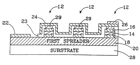
FIGs. 1 and 2 show one embodiment of the new LED 10
constructed in accordance with the present invention. It
includes an array of micro-LEDs 12 with each micro-LED 12
being isolated and having its own active layer of
semiconductor material 14 sandwiched between two
oppositely doped layers 16 and 18. In the preferred
micro-LED, the top layer 16 is p-type and the bottom
layer 18 is n-type, although opposite doping in the
layers 16, 18 will also work.
The new LED also includes a first spreading layer 20
that spreads current from the n-contact pad 22 to each
micro-LED's bottom layer 18. The contact pad 22 i s
CA 02393007 2002-05-29
WO 01/41219 10 PCTIUSOO/32084
referred to as the n-contact pad because in the preferred
em: odiment the bottom layer 18 is n-type. An insulating
layer 23 is deposited over the micro-LED array, covering
each micro-LED and the surface of the first spreader in
the gaps between the micro-LEDs. A second spreading
_aver, preferably in the form of an interconnected
current spreading grid 24, is deposited on the insulating
layer with the grid's conductive paths passing over the
micro-LEDs. A p-contact 26 is deposited on the grid 24
and current from the contact spreads through the grid to
top laver 16 each micro-LED 12. The contact 26 is
referred to as the p-contact because in the preferred
embodiment the top layer 16 is p-type.
A hole is formed through the insulating layer on top
is of each micro-LED and a micro-LED contact 29 is included
in each insulating layer hole to provide contact between
the grid 24 and the micro-LED's top layer 16. The micro-
LEDs (except for the holes) and the surface of the first
spreading layer are electrically isolated from the
current spreading grid by the insulating layer 23. The
entire structure is formed on a substrate 28 and the
micro-LEDs form an array that emits light when a bias is
applied across the contacts 22 and 26. In another
embodiment, a transparent conductive sheet is used as the
second spreader in place of the grid 24.
The new LED 10 has enhanced light emission because
of the increased emission surface area provided by the
isolated micro-LEDs. Light generated from each micro-
LED's active layer interacts with the edge of the micro-
LED after only a very short distance. If the light is
within the critical angle, it escapes from the micro-LED
and contributes to the LED's light emission. The new LED
is especially useful for LED structures in which a
CA 02393007 2002-05-29
WO 01/41219 11 PCTIUS00/32084
portion of emitted light cannot be transmitted to the
substrate due to total internal reflection (TIR) at the
current spreader-substrate interface. This is th e
situation for GaN-based LEDs on sapphire, A1N, or Mg O
suns Crates .
The new LED 10 is manufactured by first depositing
the first spreader layer 20 on the substrate 28. An
epitaxially grown LED structure with an n-type, p-type
and an active layer, is then formed on the first spreader
layer 20. The micro-LEDs are formed from the LED
structure by etching away portions of the structure using
semiconductor etching techniques such as wet chemical-
etching, RIE, Ion Milling, or any other technique used
for removing semiconductor material.
Each remaining micro-LED forms an independent and
electrically isolated device having an .active layer
surrounded by oppositely doped layers 16 and 18. The
shape and position of the micro-LEDs 12 can be varied
with the preferred shape of each micro-LED being
cylindrical. When viewed from above, each micro-LED
appears circular with a diameter of between 1 and 50
microns. The micro-LEDs are preferably formed in a close
packed pattern to maximize the usable micro-LED space.
The separation between adjacent micro-LEDs is preferably
in the range of 1 to 50 m, although the separation is
not critical to this invention. The insulator layer 23
is deposited over the entire structure by various methods
such as evaporation, CVD or sputtering. Openings are
then etched in the insulator layer 23 above each micro-
LED 12. The micro-LED contacts and the electrically
conductive grid are then deposited by standard deposition
techniques.
The first spreader layer 20 may be either a
CA 02393007 2002-05-29
WO 01/41219 12 PCT/USOO/32084
conductive layer deposited on the substrate or the
substrate itself, if it is conductive. Preferred
conductive substrates for GaN-based LEDs include GaN or
S11--con Carbide (SiC) . SiC has a much closer crystal
lattice match to Group III nitrides such as GaN and
results in Group III nitride films of high quality-
Silicon carbide also has a very high thermal conductivity
so that the total output power of Group III nitride
devices on silicon carbide is not limited by the thermal
dissipation of the substrate (as is the case with some
devices formed on sapphire) . SiC substrates are available
from Cree Research, Inc., of Durham, North Carolina and
methods for producing them are set forth in the
scientific literature as well as in a U.S. Patents, Nos.
Re. 34,861; 4,946,547; and 5,200,022.
If the substrate is the current spreading layer, the
bottom contact can be deposited by metalization on any of
the substrate's exposed surfaces. The preferred LED has
micro-LEDs 12 that are AlGaInN based with a p-type
surface as its top layer 16. The substrate is sapphire,
the first spreader is n-type AlGaInN (or an alloy
thereof), and the contact metalization is Al/Ni/Au,
Al/Ti/Au, or Al/Pt/Au. The insulating layer 23 can be
made of many materials such as, but not limited to, SiN,
SiO2, or A1N.
The grid 24 can be any electrically conductive
material including metals, semi-metals, and
semiconductors. It can be made of Al, Ag, Al/Au, Ag/Au,
Ti/Pt/Au, Al/Ti/Au, Al/Ni/Au, Al/Pt/Au or combinations
thereof. Alternatively, the grid can be made of a thin
semi-transparent metal such as Pd, Pt, Pd/Au, Pt/Au,
Ni/Au, NiO/Au or any alloy thereof. The grid 24 can be
deposited on the new LED by many conventional methods
CA 02393007 2002-05-29
WO 01/41219 13 PCT/USOO/32084
*i _r, the preferred methods being evaporation or
sputtering. in the preferred embodiment, the paths of the
current spreading grid 24 are between 1 and 10 m wide.
~he micro-LED contacts 29 can be made of Pt, Pt/Au, Pd,
Pa; Au, Ni/Au, NiO, or NiO/Au. The p-contact 26 can be
aeposlted on the interconnected grid 24 in various
locations to allow current from the contact to spread
throughout the grid.
FIG. 3 shows a second embodiment of the LED 30
constructed in accordance with the present invention,
utilizing flip-chip mounting. As above, micro-LEDs 32 are
formed in an array by etching away semiconductor material
of a full LED structure. Each micro-LED 32 has an active
layer surrounded by two oppositely doped layers. The
micro-LED arrangement and size is similar to the
embodiment described above. However, in this embodiment
each of the micro-LEDs has angled side surfaces and their
top layer is narrower than its bottom layer. Like above,
the micro-LED array is formed on a first spreader layer
34 that is formed on a substrate 36. An insulating layer
38 covers the micro-LEDs and the surface of the first
spreader between adjacent micro-LEDS. On each micro-LED
32, a hole is included in the insulating layer for a top
contact 40 A second spreader layer 42 coats the entire
micro-LED array to interconnect the top contacts 40.
The surface of the second spreader 42 opposite the
micro-LEDs is bonded to a reflective metallic layer 48 on
a submount 46 by a bonding media. A p-contact 44 is
included on the metallic layer 48 and current applied to
the second contact spreads throughout the second
spreader, to the top contacts 40 and to the top layer of
the micro-LEDs 32. There is a break in the metallic layer
48 and the n-contact 50 is formed on the portion of the
CA 02393007 2002-05-29
WO 01/41219 14 PCTIUSOO/32084
metallic layer 48 that is electrically isolated from the
portion havina the p-contact. The finger 49 is bonded
between the submount and the first spreader and conduct --s
current from the contact 50 through the metallic laye r
45, tr.rougr the finger and to the first spreader 34. The
current then spreads throughout the first spreader and to
the bottom layer of the micro-LEDs.
In this flip-chip embodiment, light from the LED 50
is primarily emitted through the substrate 36. The second
spreader 42 can be optically reflective so that light
emitted from the micro-LEDs 32 in the direction of the
second spreader 42 is reflected towards the LED' s
substrate 36. Al or Ag is preferably used as the second
spreader and each micro-LED 32 is AlGaInN based with a p-
type top layer. Each top contact 40 is preferably Pt,
Pt/Au, Pd, Pd/Au, Ni/Au, NiO, or NiO/Au.
This embodiment provides increased sidewall
interaction with the emitted light as a result of the
isolated micro-LEDs. The portion of the second spreader
42 that is disposed between the micro-LEDs functions as
LEEs by reflecting light from the micro-LEDs toward the
substrate. This configuration also provides improved heat
transfer out of the new LED chip through the submount.
Figs. 4 and 5 show another embodiment of the new LED
51 that does not have an insulator layer to isolate the
first spreader from the second. Instead, micro-LEDs 52
are connected to adjacent micro-LEDs by conductive paths
53 of an interconnected grid 54, wherein the paths have
semiconductor material below them. Each opening 55 in the
grid 54 is an area where semiconductor material was
etched from the LED structure when manufacturing the LED
50. Portions of the structure remain under the grid 54 as
micro-LEDs 52 and as semiconductor material under the
CA 02393007 2002-05-29
WO 01/41219 PCT/US00/32084
grit paths 53 between the micro-LEDS. The micro-LEDs and
the :nateria- under the paths comprise an active layer
surrounded cy two oppositely doped layers, with the
entire structure formed on a first spreader layer 56 and
substrate 56.
first contact 60 is deposited on the firs t
spreader to apply current to the bottom layer of the
micro-LEDs and a second contact 62 is included on the
current spreading grid to spread current to the top layer
10 of the micro-LEDs. When a bias is applied across the
contacts 60 and 62, current is applied to the micro-LEDs
and the semiconductor material under the conductive
paths, all of which emit light. Light escapes from the
side surfaces of the micro-LEDs material under the paths,
15 avoiding total internal reflection. This technique is
therefore generally applicable to any LED structure on
any substrate and is implemented with standard processing
techniques.
The LED 51 is manufactured by first depositing the
first spreader layer 56 on the substrate 58, and then
forming a continuous LED structure that covers the
current spreading layer 56. The grid 54 is deposited on
the LED structure and portions of the LED structure that
are visible in the grid openings are etched away by
various methods such as wet chemical etching, Reactive
Ion Etching (RIE) , Ion Milling, or any other technique
used for removing semiconductor material. Portions of the
LED structure are also etched to provide an area for
contact pads 60, and contact pads 60 and 62 are
deposited. The grid 54 can be made of any electrically
conductive material including but not limited to metals,
semi-metals, and semiconductors or combinations thereof.
The preferred micro-LEDs are GaN-based with each micro-
CA 02393007 2002-05-29
WO 01/41219 PCT/US00/32084
16
LED's top layer 55 being a p-type AlGaInN or any allay
thereof, and the grid 54 is preferably made of a thin
meta' such as Ni, Pd, Au, Pt or any combination thereof.
The dashed line in FIG. 4 illustrates one of the
.ml pro-LEDs and the area around the micro-LED where LEES
can be included to further enhance light extraction as
more fully described below.
FIGs. 6 and 7 show two additional embodiments 70 an
80 of the, new LED with different micro-LED and grid
patterns 72 and 82, although many different patterns can
be used. Each embodiment has a respective bottom
spreading contact 73 and 83. In FIG. 6, the micro-LEDs 74
are interconnected crosses with current spreading to each
of the micro-LEDs through the various paths. Each path
has semiconductor material below it to isolate it from
the first spreader layer. The grid 72 provides a square
array pattern of openings for light interaction.
The grid 54 has an advantage over grid 72. In LED
70, TIR light can reflect down one of the grids numerous
conductive paths and reflect within the LED without
interacting with a surface of one of the micro-LEDs.
Optical loss present in the grid or underlying layers
will cause some of this TIR light to be absorbed before
it can escape out the final edge of the new LED. The grid
54 reduces this problem because light emitting from the
micro-LEDs will reach a side surface after travelling
only a short distance (at most two micro-LED lengths),
thereby increasing the light out of the device.
In FIG. 7 the micro-LEDs are randomly shaped and
have random interconnecting paths. Again, the paths have
semiconductor material below them. The random pattern
reduces the number of paths for the TIR to travel before
it will encounter one of the micro-LEDs in one of the
CA 02393007 2002-05-29
WO 01/41219 PCT/US00/32084
1%
grid openings. Like above, the dashed lines around the
micro-LEDs in FIG. 6 and " illustrate the micro-LED 76
anc 86 with LEEs around their perimeters, as more full -v
described below.
Opening sizes and distances between openings are
preferably between 1 and 30 um, but may be larger or
smaller. The pattern of the openings may be aperiodic or
periodic since the nature of the light interaction with
the micro-LED edges does not require either condition.
In the preferred embodiment on a p-type AlGaInN layer,
the grid openings are between 1 micron and 20 m and the
micro-LEDs have a width between 1 m and 30 pm
All of the previous three embodiments can be
integrated with LEEs between micro-LEDs to further
increase light emission. The LEEs can either be formed on
the side surfaces of the micro-LEDs or on the surface of
the first spreader layer or the conductive substrate in
those embodiments having no first spreader layer.
FIG. 8 shows several alternative shapes of LEEs that
are included as embodiments in this invention, although
other shapes can be used and the scope of this invention
is not limited to the shapes shown. LEEs 82, 84, 86 have
curved surfaces while the LEEs 88, 90, 92, 94 have
piecewise linear surfaces. Alternatively, the LEE may be
a randomly roughened layer that acts as a light
disperser.
The LEEs can be formed by standard etching
techniques such as wet chemical etching, RIE, or ion
milling. In the preferred embodiment, the LEEs are formed
by using a commercially available polymer (such as a UV
or e-beam sensitive photoresist) as an ablative etch
mask. This polymer is first deposited and patterned with
CA 02393007 2002-05-29
WO 01/41219 18 PCT/US00/32084
square-like edges. The polymer is heated to a temperature
and reflows like glass to give a gradual linear or curved
shape to the edges of the polymer. The polymer thickness,
pattern shape, heating temperature and heating time will
derermlne the edge shape. The pattern is transferred to
the AlGaInN based micro-LEDs with RIE. Linear and curved
LEES are easily fabricated by this method and piecewise
linear LEEs can be easily formed by using multiple
ablative masks.
A second technique for forming LEEs is to use a
negative polarity UV-exposable photoresist. First, the
photoresist is exposed for a particular exposure time and
is treated to produce a negative polarity. The
photoresist is then developed to produce an undercut
curved or linear shape in its profile. This pattern can
then be transferred to the semiconductor material through
a dry etching technique. For both embodiments, the dry
etching conditions will also impact the final shape of
the lens in the semiconductor material.
FIGs. 9-15 show embodiments of the new LED with LEEs
integrated within the micro-LED array in a variety of
ways to enhance light extraction. These embodiments
represent a few of the possible ways that the LEEs can be
used in accordance with this invention, and the scope of
this invention is not limited to the described
embodiments.
FIG. 9 shows a new LED 100 that is similar to the
LED 50 in Figs. 4 and 5, but has LEEs 101, 102, 103
between the micro-LEDs 104. The LEEs 101, 102, 103 allow
light that is directed through a micro-LED's side surface
to reflect off the LEEs and be re-directed away from the
substrate into a package. Light rays that reflect off of
the interface between the substrate 108 and first
CA 02393007 2002-05-29
WO 01/41219 9 PCT/US00/32084
1
spreader laver 106 through TIR can. also interact with the
LEES 101, 102, 103 to escape into the package, providing a
higher light output. The LEEs depicted in FIG. 8 can be
e:.tner deposited onto or processed into the new LED. As
described above, the depth of the LEEs can also be varied
with the preferred depth in the range of 0 . 5 m to 10
m..
FIG. 10 shows a new LED 110 similar to the LED 100
in FIG. 9, but having randomly roughened dispersion LEEs
112 between the micro-LEDs 113. The light interaction
with the roughened layer allows TIR light to reach the
surface within its critical angle and escape before being
absorbed. In the preferred embodiment, the roughened
surface is formed ..by using polystyrene or silica
microspheres as an etch mask to transfer micro-scale
roughness into the semiconductor. The depth and width of
the random roughness may be less than 20nm to more that
500nm, with the preferred size being on the order of the
wavelength of light generated by the LED.
FIG 11 shows a new LED 120 that is similar to LED
110 in F.G. 10, but includes a current blocking layer
within the micro-LED. The blocking layer 122 directs
current flow underneath the dispersive LEE 124,
increasing the chance for light to interact with the LEE
and escape.
As an alternative to forming the LEEs between the
micro-LEDs, the LEEs can be formed directly on the micro-
LED side surfaces. FIG 12 shows a new LED 130 that is
similar to the LEDs in FIGs. 9, 10 and 11, but having
various LEEs 131-133 formed directly on each micro-LED' s
side surfaces. The LEEs can be formed using the same
methods as described above. Light that travels towards
CA 02393007 2002-05-29
WO 01/41219 20 PCTIUSOO/32084
the micro-LED side surfaces is redirected in directions
that cause light to escape out one of the surfaces of the
substrate 134, through the first spreader layer 135, or
through the micro-LEDs 132. Light that is reflected backrc7. one suostrate 134
also has an increased chance of
escape -:due t the LEEs on the micro-LED edges.
T G 13 shows a new. LED 140 where curved LEEs 142 ar e
formed on the side surfaces micro-LEDs 144. The curved
LEEs 142 provide the additional advantage of focusing the
LED light into a more well defined direction. The depth
and width of the LEEs 142 can be varied with the
preferred depth of any one LEE being 0.1 gm to 50 gum.
Two additional embodiments are shown in FIGs. 14 and
15. Figure 14 shows a new LED 150 with a combination o E
curved LEEs 152 on the side surface if the micro-LEDs 154
and full curved LEEs 156 between the micro-LEDs 154. The
LEEs work together to enhance light extraction by
refracting and reflecting light out of the LED package
FIG. 15 shows new LED 160 with curved LEEs 162 on
the side surfaces of the micro-LEDs 164, using flip-chip
embodiment mounting similar to the embodiment shown in
FIG 3. The second spreader 164 is reflective and the
substrate 166 is the primary emitting surface. The LEEs
162 and the portions of the second spreader 164 work
together to enhance light extraction by refracting and
reflecting light out of the LED package through the
substrate.
Although the present invention has been described in
considerable detail with reference to certain preferred
configurations thereof, other versions are possible. For
instance, the bottom layers of the micro-LEDs in the
array can be in contact. The light extraction structures
can also be used in many different combinations and can
CA 02393007 2002-05-29
WO 01/41219 2 PCT/USOO/32084
be many different shapes and sizes. Also, the LED
structure aescribed above can have more than one active
laver sandwiched between oppositely doped layers.
Therefore, the spirit and scope of the appended claims
should not be limited to their preferred embodiments
describes above.