Note: Descriptions are shown in the official language in which they were submitted.
CA 02393330 2002-06-03
WO 01/55473 PCT/USO1/00861
MANUFACTURING MEDICAL DEVICES BY VAPOR DEPOSITION
FIELD OF THE INVENTION
The present invention relates to medical devices and, more particularly, to
medical devices having improved mechanical properties that are formed using
vapor
deposition techniques.
BACKGROUND OF THE INVENTION
Implantable medical devices such as scents, blood filters, artificial heart
valves
and the like are typically subjected to hostile working conditions. Fox
example, stems
and blood filters are introduced into the body while in a compressed shape and
are
thereafter expanded via self expansion or mechanical expansion to a final,
useful shape
when positioned to a taxget location within the body. After deployment, the
devices
should have sufficient physical, biological and mechanical properties to
perform
throughout the expected useful lifetime. Moreover, implantable medical devices
are
typically characterized by complex, intricate shapes and strict dimensional
and
compositional tolerances.
In view of the stringent requirements of medical devices, the processes used
to
form these devices must be accurate and reproducible, and obtain the desired
dimensional, compositional and mechanical properties. Conventional production
processes, however, are often complex and expensive. For example, conventional
processes used to produce patterned stems often start with wire, tube or sheet
materials.
Typical processing steps to produce a patterned stmt from a wire may include
winding
the wire around a mandrel into a complex configuration, welding the wire at
certain
~,5 junctions, and heat treating the wire to create the final patterned
device. To produce a
patterned' stmt from a tube or sheet, conventional processes may include steps
such as
stamping, cutting or etching a pattern into the starting material, expanding
and/or
CA 02393330 2002-06-03
WO 01/55473 PCT/USO1/00861
rolling the starting material into a suitable stmt shape, and heat treating to
create the
final device.
Most of the manufacturing steps associated with these conventional methods
introduce defects into the metallic structure of the formed device. The
defects can
include excessive oxidation, localized deformation, surface flaws and the
like. These
defects often reduce desired properties, such as strength, fatigue resistance
and
corrosion resistance.
The performance properties of the medical device are not only effected by
manufacturing-processes, but are also effected by the material properties of
the raw
material. For instance, if the wire or tube used to form a medical device
contains
material or structural defects, the formed medical device may also often
contaiil similar
or greater defects. Some defects in the formed device may be reduced by
techniques,
I S such as annealing, but these techniques often impart other undesirable
effects. For
instance, annealing often requires high temperature treatment of a metallic
device to
recrystallize its microstructure to reduce grain size and residual stress.
Such a high
temperature treatment can often impart physical deformation of the device due
to
thermal heating and cooling steps or due to the change in the microstructure
itself.
Because medical devices often require intricate shapes and strict dimensional
tolerances, physical deformation of the device during manufacturing is often a
problem.
Furthermore, the compositional properties of the raw material used to form the
medical device also effects the final properties of the device. Impurities
often degrade
useful mechanical properties, reduce corrosion resistance and effect the
biocompatability of the medical device.
Accordingly, a need exists for a manufacturing process to form a medical
device
without the disadvantages of the prior art. Furthermore, a need exists for a
medical
device with improved biocompatability and mechanical properties.
2
CA 02393330 2002-06-03
WO 01/55473 PCT/USO1/00861
In view of the shortcomings of conventional medical device manufacturing
processes, there exists a need for a process that facilitates the reproducible
production
of medical devices having improved mechanical properties.
SUMMARY OF THE INVENTION
In one aspect, the present invention provides a method of forming a medical
device, the method including the steps of providing a source of biocompatible
metal;
providing a substrate; depositing a biocompatible metallic layer on the
substrate from
the source by a vapor deposition process; and removing the metallic layer from
the
substrate. The metallic layer thus removed is the medical device or serves as
a basis for
forming the medical device.
In another aspect, the present invention includes a medical device formed by
the
process of the present invention. The medical devices have at least one or
more
members formed from biocompatible metals.
The medical devices also have a crystallographic structure that is produced by
the vapor deposition methods of the present invention. Desirable
crystallographic
structures include amorphous, nanocrystalline and monocrystalline structures.
Furthermore, the medical devices may include monoisotopic metal or alloys of
monoisotopic metals.
BRIEF DESCRIPTION OF THE DRAWINGS
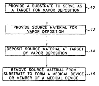
Figure 1 shows a schematic of a method for forming a medical device according
to a vapor deposition method of the present invention.
Figure 2 shows a medical device formed according to a vapor deposition
method of the present invention.
Figure 3 shows a second medical device formed according to a vapor deposition
method of the present invention.
3
CA 02393330 2002-06-03
WO 01/55473 PCT/USO1/00861
Figure 4A shows an example of a vapor deposition apparatus in accordance with
an embodiment of the present invention.
Figure 4B shows the vapor deposition apparatus of Figure 4A with mass
analysis ans separation in accordance with an embodiment of the present
invention.
Figure 5 shows a substrate having a deposition layer, in accordance with an
embodiment of the present invention.
Figure.6A depicts a cross sectional view of the substrate with a deposition
layer
of Figure 5 taken along the 6-6 axis.
Figure 6B shows a mufti-layered substrate, in accordance with another
embodiment of the present invention.
Figure 7 shows the cross sectional view of deposition layer of Figure 6 after
removal of the substrate.
Figure 8 shows a mufti-layered substrate having a release layer, in accordance
with another embodiment of the present invention.
Figures 9 and 10 show side and end views, respectively, of an example of a
deposition mask used in accordance with an embodiment of the present
invention.
Figure 11 shows a portion of a patterned substrate having a vapor deposited
metallic layer, in accordance with an embodiment of the present invention.
Figure 1? shows a portion of a second patterned substrate having a vapor
deposited metallic layer, in accordance with an embodiment of the present
invention.
4
CA 02393330 2002-06-03
WO 01/55473 PCT/USO1/00861
Figure 13 shows a portion of the patterned substrate of Figure 11 after
removal
of a portion of the metallic layer.
Figure 14 shows a stmt wire for use in forming the medical device of Figure 3,
in accordance to an embodiment of the present invention.
Figure 15 shows an example of a vapor deposition apparatus for forming the
stmt wire of Figure 14, in accordance with an embodiment of the present
invention.
DETAILED DESCRIPTION OF THE INVENTION
The present invention overcomes many of the difficulties associated with
conventional medical devices and the methods used to form such medical
devices. By
using vapor deposition techniques for the formation of medical devices, the
composition, thickness, surface roughness, and microstructure of devices
formed in
accordance with the present invention are accurately and precisely controlled.
The
medical devices formed by the process of the present invention are tailored to
have
desired compositions, mechanical properties, and geometries.
In one aspect as illustrated in Figure 1, the present invention is directed to
a
method of forming a medical device, the method including the steps of
providing a
substrate and source material, depositing a metallic layer of source material
on the
substrate by a vapor deposition process and removing the metallic layer of
source
material from the substrate.
At step 10, a substrate is provided to serve as a target for source material
by
vapor deposition. As described fiuther herein, the material of the substrate
and the
configuration of the substrate are selected according to the desired aspects
of the
medical device or medical member formed by the process of the present
invention.
CA 02393330 2002-06-03
WO 01/55473 PCT/USO1/00861
At step 12, a source material for vapor deposition is provided. Desirably, the
source material is biocompatible material, as described further herein,
suitable for use
as a medical device.
At step 14, source material is deposited as a metallic layer at the target or
onto
the substrate by a vapor deposition process.
At step 16, the metallic layer from the substrate is removed. The metallic
layer
thus removed is the medical device or serves as a basis for forming the
medical device.
In another aspect, the present invention includes medical devices made by the
process
of the present invention.
"Vapor deposition," as used herein, refers to any process of depositing metals
and metal compounds from a source to a substrate or target by dissipating
metal ions
I S from the source in a vaporous medium. Examples of useful vapor deposition
processes
for use in the present invention include physical vapor deposition processes
such as
evaporation, and sputtering. Direct and assisted ion beam deposition, and
chemical
vapor deposition are also useful. These useful vapor deposition processes are
generally
described below.
In the evaporation process, vapor is generated by heating (e.g., by electron
beam
interaction) a source material to a temperature to cause the vaporization
thereof. The
evaporating metal atom leaves the surface of the source material in a straight
line.
Therefore, highest quality deposition layers are deposited when the source-to-
substrate
distance is less than the mean path distance between collisions of the
vaporized metal
and the surrounding vacuum chamber. At chamber pressures greater than 10-1 Pa,
a
useful source-to-substrate distance is generally less than 500 mm. At 10-' Pa,
this
distance can be increased to over 4000 mm. Furthermore, it is useful to rotate
or
translate the substrate within the suitable source-to-substrate distance to
ensure that the
entire surface of the substrate is coated. Deposition rates using commercially
available
equipment typically exceed 0.05 mm per minute.
6
CA 02393330 2002-06-03
WO 01/55473 PCT/USO1/00861
In the sputtering process, a source is bombarded with ions of an inert gas to
cause the dislodgment of material therefrom. The source of ions is typically
an ion
beam or plasma discharge. In this technique, a source material is placed in a
vacuum
chamber with a substrate material. The chamber is evacuated to 10-3 - 10-5 Pa,
and
backfilled with an inert gas such as argon to a pressure of 0.1 - 10 Pa to
sustain a
plasma discharge. The substrate is made positive, relative to the source
material, by a
radio-frequency power source. When the applied potential reaches the
ionization
energy of the gas, electrons, generated at the cathode, collide with the gas
atoms,
ionizing them and creating a plasma. These positively charged ions, having
high
kinetic energy, are accelerated toward the cathode source material, thus
dislodging
atoms that then travel across the electrode gap. These dislodged atoms are
then
deposited onto the substrate. Because of the energy of these atoms, their
adherence to
the substrate is generally better than if they were deposited by vacuum
evaporation.
Ion beam assisted deposition (IBAD) utilizes a high energy beam of heavy ions
to help density the deposited metals, such as metals deposited by sputtering
or
evaporation processes.
A useful ion beam assisted deposition method further includes mass analysis of
the ion beam before the ionized source material is deposited onto the
substrate. This
method accelerates the ion beam and passes it through a filter typically
containing
magnetic and/or electrostatic fields to separate different mass-weight
species. This
filter is often referred to as an ExB filter and is commercially available.
Those of skill
in the art can select an ExB filter with desirable features to be useful with
the present
invention. A particular mass-weight species is then targeted at the substrate.
When the
ion sources are individual pure element ingots, this technique can be used to
separate
the isotopes of an element and to direct a particular isotope to the
substrate. Because
naturally occurring elements typically consist of a range of atomic weights or
isotopes
(See Table 1 below), this method is useful in selecting a particular isotope
for forming a
medical device. For instance, titanium with atomic weight of 48 may be
selected for
7
CA 02393330 2002-06-03
WO 01/55473 PCT/USO1/00861
vapor deposition while rejecting titanium with atomic weights of 46, 47, 49
and S0.
Furthermore, other impurities, such as oxygen, that may be contained in the
elemental
ingot may be filtered away from the substrate with this method.
TABLE 1: Naturally Occurring Isotopes of Ti &Ni
S
Element Atomic No. Atomic Weight Natured Occurrence
Titanium 22 46 7.9
(22T1~7.96)47 7.3
48 73.9
49 S.S
SO S.4
Nickel 28 S8 67.8
(ZSNiss.?)60 26.2
.
61 1.2
62 3.7
64 1.1
The removal of impurities and the filtering of particular isotopes are useful
in
the present invention. The crystalline structure of the metallic medical
article may be
affected by impurities. Single crystal or monocrystalline materials are more
easily
formed when levels of impurities are minimized. Furthermore, medical devices
formed
as a monocrystalline, monoisotopic material are useful with the present
invention.
Large, single crystals of metals can be grown by a number of methods. One
simple method is to melt the metal in a conical vessel, and then lower the
vessel slowly
1 S from the furnace, point first. Under controlled temperature conditions a
single seed
forms at the point of the cone and continues to grow until it fills the cone
or unit crystal
growth is otherwise terminated. The single crystal may also slowly be drawn
from the
vessel as to make a filament of a single crystal. Impurities in the vessel
often terminate
single crystal growth. Nevertheless, a single crystal filament or wire may
suitable be
formed. The present invention, however, is not limited to "melting" techniques
for
forming single crystals and other methods may suitable be used.
8
CA 02393330 2002-06-03
WO 01/55473 PCT/USO1/00861
Such a single crystal filament or wire may then be used as a substrate in a
vapor
deposition process. Ionized metal atoms deposit on this substrate and may form
the
same crystalline structure, i.e., monocrystalline structure, as contained in
the substrate.
Ion beam deposition with mass analysis is a useful vapor deposition process to
form
monocrystalline medical devices because impurities and mass-species can be'
controlled. In such a manner a monoisotopic, monocrystalline medical article,
such as a
stmt or a stmt wire, may suitably be formed.
Another useful method of the present invention for forming medical devices is
crystallization of structures formed with an amorphous morphology. An
amorphous
metallic structure may be deposited onto a substrate by vapor deposition when
the
substrate is a dissimilar material from the deposited material. The amorphous
structure
may subsequently be treated or aged under conditions that are well below
typical
annealing temperatures, such as about or near room temperature, to form a
monocrystalline metallic structure. Ion beam deposition method is useful
because
impurity levels can be substantially reduced as compared to other methods.
Reduced
impurity levels facilitate the growth of single crystals. Moreover,
monocrystalline and
monoisotropic crystals can be suitably formed by vapor deposition methods,
especially
by ion beam depositions with mass analysis.
Furthermore, as compared to conventional processes, enhanced mechanical
properties for medical devices can be obtained by minimizing the grain size of
the
metallic structure. Conventional grain sizes are on the order of ten microns
or larger. A
medical device with a nanocrystalline structure is useful because of its
enhanced
mechanical properties, for instance fatigue resistance and corrosion
resistance. A
nanocrystalline structure in a biocompatible material with a grain size
ranging from
about 1 to 500 nanometers is useful as a medical device. Also useful is a
biocompatible
material with a grain size of about 1 to 100 nanometers. Furthermore, a
nanocrystalline
structure in a biocompatible material with a grain size of about 1 to 50
nanometers is
useful as a medical device. Moreover, a biocompatible material with a grain
size of
about 1 to 10 nanometers is also useful as a medical. .
9
CA 02393330 2002-06-03
WO 01/55473 PCT/USO1/00861
Such nanocrystalline structures can be formed by depositing an amorphous layer
of desired material onto a substrate or target. The above-described aging
techniques
can be used to form manometer sized crystals. Furthermore, the orientation of
the
manometer sized grains can be controlled to yield a orderly grain structure
with
substantially similar crystal orientation. A useful method for forming such
structures is
through epitaxy where desired material is deposited onto a substrate having a
crystalline
structure, such as an orientated, nanocrystalline structure, and the deposited
material
forms a crystalline structure similar to that of the substrate.
The present invention is described with reference to the formation of a
metallic
stmt, although it should be understood that the process of the present
invention cari be
used to form any applicable medical device such as, for example, blood filters
and
artificial heart valves. Furthermore, the medical devices of the present
invention have
at least one or more metallic members. These members have discrete dimensions
and
shapes as desired for particular medical devices and for particular medical
applications.
Various stmt types and stmt constructions may be employed in the invention.
Examples of the various stems include, without limitation, self expanding
stems and
balloon expandable stems. The stems may be capable of radially contracting, as
well,
and in this sense can be best described as radially or circumferentially
distensible or
deformable. Self expanding stems include those that have a spring-like action
which
causes the stmt to radially expand, or stents which expand due to the memory
properties of the stmt material for a particular configuration at a certain
temperature.
Nitinol is one material which has the ability to perform well while both in
spring-like
mode, as well as in a memory mode based on temperature. Other materials are of
course contemplated, such as stainless steel, platiniun, gold, titanium and
other
biocompatible metals.
The configuration of the stmt may also be chosen from a host of geometries.
For example, wire stems can be fastened into a continuous helical pattern,
with or
CA 02393330 2002-06-03
WO 01/55473 PCT/USO1/00861
without a wave-like or zig-zag in the wire, to form a radially deformable
scent.
Individual rings or circular members can be linked together such as by struts,
sutures,
welding or interlacing or locking of the rings to form a tubular stmt. Tubular
slotted
stems are also useful in the present invention.
In one aspect of the present invention, a metallic scent, such as a slotted
metallic
stmt I00 as depicted in Figure 2 or a wire-framed metallic stmt 200 as
depicted in
Figure 3, is formed according to an embodiment of the present invention. As
depicted
in Figure 4A, a mandrel I05 is placed a vacuum chamber 110 or other suitable
device
for vapor deposition processes. The mandrel 105 is, for example, a metallic
wire or any
other suitable cylindrical element.
The mandrel 105 is desirably mounted onto a motor driven rotary mount 106 to
assist in the production of a uniform deposition. During deposition, the
rotary mount
106 rotates, as depicted by vector A, at a speed determined by the medical
device
equipment and process parameters, for instance about I-60 rev/min. After
forming an
appropriate vacuum pressure in the chamber 110, the vapor deposition process
commences whereby a metallic layer 115 is deposited onto the mandrel 105 as
shown
in Figure 5. The source of the material deposited as the metallic layer 115 is
source
material 120 that is placed the vacuum chamber 110. The vapor deposition
process
continues until the metallic layer 115 achieves a desired thickness. As
described by the
aforementioned vapor deposition techniques, metallic layer 115 can be formed
to have
a range of crystalline morphologies, including a monocrystalline or a
nanocrystalline
morphology.
Metallic layer 115 may also be formed as having a monoisotopic morphology
through use of mass analysis of an ion beam before the ionized source material
is
deposited as metallic layer 115. As depicted in Figure 4B, vacuum chamber 110
may
further include filter 180 and templates 181 and 182, interrelated as shown.
Filter 180
may be used to separate the isotopes of an element or contaminants that may be
present
in source material 120. Desirable filter 180 is a filter containing magnetic
and/or
11
CA 02393330 2002-06-03
WO 01/55473 PCT/USO1/00861
electrostatic fields, such as an ExB filter. Templates 181 and 182 are useful
for
targeting a particular isotope toward mandrel 105 while preventing other
isotopes or
contaminants from reaching mandrel 105. For example, as depicted in Figure 4B,
beam
190 contains a particular isotope of source material 120 to be deposited on
mandrel
105. Other beams, such as beams 191 A-D, contain other isotopes or
contaminants of
source material 120 and these other beams are prevented from reaching mandrel
105
through use of templates 181 and 182.
Following deposition, the coated mandrel 105 is removed from the chamber
110. The top and bottom ends 107, 108 of the coated mandrel 105 are removed by
any
suitable means such as, for example, cutting with a low-speed cutting saw
equipped
with a diamond-impregnated copper cutting wheel. Alternatively, multiple cuts
can be
made of a relatively long coated mandrel to yield numerous coated mandrel
portions,
each of which is used to form a stmt.
As depicted in Figure 6A, which is a cross sectional view of the coated
mandrel
105 taken along the 6-6 axis, the metallic layer 115 encompasses mandrel 105.
To
form a medical device or a member of a medical device the metallic layer 115
is
removed from mandrel 105. The metallic layer 115 is removed from the coated
mandrel 105 by any suitable technique such as, for example, exposing the
coated
mandrel 105 to a solution which will dissolve the mandrel material but not the
metallic
layer 115. As an example, when the mandrel 105 is a low carbon steel wire and
the
metallic layer 115 comprises nitinol, the mandrel 105 may be dissolved with a
suitable
acid, such as hydrochloric acid, which does not destroy the metallic layer 115
to form a
medical device or member. Figure 7 depicts a view of the metallic layer 115 of
Figure
6A after the mandrel 1 OS has been removed.
As an alternative, the metallic layer 115 may be removed from the mandrel 105
by machining techniques such as, for example, drilling, grinding, milling,
laser cutting,
laser milling and the like.
12
CA 02393330 2002-06-03
WO 01/55473 PCT/USO1/00861
As another alternative, a release layer 130 is formed between the mandrel 105
and the metallic layer 115 as shown in Figure 8. The release layer 130 is
applied to the
mandrel 105 by any suitable coating technique such as, for example, dipping,
spraying,
rolling, electroplating, vapor deposition and the like. After deposition of
the metallic
layer 115, the release layer 130 is removed by machining or, desirably, by
dissolving it
in a solution that attacks the material of the release layer 130 while not
affecting the
materials of the mandrel 105 and the metallic layer 115. For instance,
sulfuric acid is a
useful release agent when the mandrel is titanium or tantalum, the release
layer is
copper and the metallic layer is nitinol.
After release from the mandrel 105 or from the release layer 130, the metallic
layer 115 either serves as a stmt or as the basis for forming a stmt by
further
processing. Desirably, a scent formed in accordance with the present invention
will
have a pattern of openings, such as openings 1 Ol in slotted metallic stent,
therein to
help facilitate expansion for deployment within a body lumen. In one aspect,
the
openings 101 in the stmt 100 are formed by machining such openings into the
metallic
layer 115 after removal from the mandrel 105.
In another aspect, a mask 150 is used to surround the mandrel 105 during
deposition of the metallic layer 115. Figures 9 and 10 show side and end
views,
respectively, of an example of the mask 150. The mask 150 is shaped as the
inverse of
the intended final stmt configuration such that the vapor deposition process
results in a
pattern of openings, such as openings 101 in slotted metallic stmt 100, in the
metallic
layer 115. A mask may also be suitably used to form other shapes or
configurations,
such as openings 210 in wire-formed metallic stmt 200.
In yet another aspect, the mandrel 105, as illustrated in Figure 11, is
patterned to
cause a corresponding pattern to be formed in the deposited metallic layer
115. Figure
11 is a partial longitudinal view of coated mandrel 105 of Figure 5 taken
along the 11-
11 axis. The pattern in the mandrel 105 may be, for example, a negative
pattern 160 in
which the intended pattern for, stmt 100 is recessed into the mandrel 105.
13
CA 02393330 2002-06-03
WO 01/55473 PCT/USO1/00861
Alternatively, the pattern in the mandrel 105 may be a positive pattern 170,
as depicted
in Figure 12, in which the intended pattern for stmt 100 is extended from the
mandrel
1 O5. Negative patterns, positive patterns or combinations thereof may be used
with the
present invention. As depicted in Figure 13, portions of the metallic layer
115 not
intended to be part of the stmt 100 is removed by any suitable process such
as, for
example, machining, etching, laser cutting and the like to form a medical
device or a
member of a medical device. The remaining portions of the metallic layer 115
in
Figure 13 may be removed from the mandrel 105 by use of the aforementioned
methods
of the present invention.
The positive and negative patterns on the mandrel are configured to produce a
reverse image of the stent on the surface of the mandrel. Machinery for
producing the
reverse image on the surface of the mandrel may vary depending on the
complexity of
the geometric pattern, type of material used for the mandrel and other
considerations.
Fine cutting heads or tools may be used to machine a pattern into the mandrel
with
micro-machining methods. Etching, molding and lasering techniques are also
usefiil
methods for forming the reverse image on the mandrel.
The reverse image which is formed on the surface of the mandrel is desirably
free or substantially free from micropores or defects because the quality of
the
subsequently vapor deposited stmt may depend, in part, on the surface quality.
Thus,
subsequent to the mechanical formation of the reverse image, chemical etching
or other
polishing techniques may be used to remove surface imperfections.
Additionally, oils,
oxides and other matter which may interfere with the quality of the vapor-
deposited
metallic layer are removed prior to the vapor deposition. Chemical and
electrochemical
cleaning may be used to so condition the surface of the micro-machined
mandrel.
In another aspect of the present invention, a fine metal wire may be used as
the
target for vapor deposition. As depicted in Figures 14 and 15, metallic layer
215 is
deposited onto wire 205 with vapor deposition methods of the present invention
to form
stmt wire 225. Wire 205 is introduced into vacuum chamber 210 through seal
231.
14
CA 02393330 2002-06-03
WO 01/55473 PCT/USO1/00861
Source material 20 is deposited by vapor deposition onto wire 205. The coated
wire
205 exits vacuum chamber 210 through seal 232. seals 231 and 232 serve to
maintain
vacuum conditions within vacuum chamber 210 as wire 205 is passed through
vacuum
chamber 210.
As depicted in Figure 15, wire 205 can be cycled through vacuum chamber 210
through multiple passes until a desire thickness of metallic layer 215 is
obtained. After
achieving the desired thickness of metallic layer 215, stmt wire 225 may
removed from
the vapor deposition process to form wire-formed metallic stmt 200, or other
medical
device. Stent wire 225 can be formed into stmt 200 by appropriate bending and
attaching, such as welding, techniques.
Metallic layer 215 can be fabricated as a single crystal material,
monocrystalline
and monoisotopic material or a nanocrystalline material by previously
described
inventive methods. Desirably, stmt wire 225 has a single crystal structure.
The material deposited as the metallic layer 115 or 215 is any suitable
material
for use in medical device applications such as, for example, nitinol,
stainless steel,
titanium, cobalt-chromium alloys, gold, platinum, niobium, zirconium, silver,
tantalum
and alloys thereof. The vapor deposition of these materials results in a
deposited
metallic layer 115 having a fine, equiaxed microstructure which may be
precisely
established as a function of process parameters. These microstructures in turn
affect
mechanical properties such as strength and corrosion resistance.
The process of the present invention is further amenable to the deposition of
multiple layers for the further improvement of desired medical device
properties. For
example, as depicted in Figure 6B, the deposited metallic layer 115 is
optionally coated
with a layer 116 of a radiopaque material such as platinum or tantalum to
impart
radiopacity to the medical device. The deposited metallic layer 115 is also
optionally
coated with a layer 117 of a material, such as carbon, to impart
thrombogenicity and
corrosion and/or fatigue resistance to the medical device. If applied to the
metallic
CA 02393330 2002-06-03
WO 01/55473 PCT/USO1/00861
layer 115, such additional coatings 116, 117 are applied singularly or in any
combination. Moreover, the additional coatings 116, 117 are desirably applied
in the
same vacuum chamber 110 used for the deposition of metallic layer 115. To
facilitate
the deposition of the additional coatings 116, 117, it is preferred that the
chamber 110
be equipped to receive and deposit multiple sources so that the additional
coatings 116,
117 can be deposited immediately following the deposition of metallic layer
115
without breaking vacuum. Alternatively, the source materials for the
additional
coatings I I6, 1 I7 may be sequentially loaded into the chamber 1 I O for
deposition.
~ Following the deposition of the metallic layer 115 and optional layers 116,
117,
the coated mandrel 105 is removed from the chamber 105. The layers 115, 116,
117
are optionally subjected to further processing steps such as, for example,
machining,
heat treating, oxidizing, welding, attaching to other components, applying
organic
coatings, and the like. If the layer 115 comprises nitinol or another shape
memory
alloy, it is subjected to thermomechanical "training" steps to induce the
shape memory
effect, as is known in the art.
The present invention is further described with reference to the following non-
limiting examples.
EXAMPT.ES
Example 1
A patterned nitinol stmt is formed according to the following processing
steps.
A steel wire mandrel measuring about 10 mrn in diameter and 30 mm in length is
placed in a vacuum chamber on a motor driven rotary mount. Also mounted in the
chamber is a nitinol source target comprising about 55.9 wt% nickel and the
balance
essentially titanium. The chamber is then evacuated to a pressure of less than
10-6 torr.
Argon is introduced into the chamber at a flow rate of 100 cm3lmin, producing
an
operating pressure of about 10 millitorr. A plasma is then generated in the
chamber by
ion bombardment of the nitinol target, resulting in nitinol deposition onto
the wire
16
CA 02393330 2002-06-03
WO 01/55473 PCT/USO1/00861
mandrel. Sputter deposition is continued until the thickness of the deposited
nitinol
layer is about 0.25 mm, after which the coated mandrel is removed from the
chamber.
The coated mandrel is cut at both ends to a length of about 20 mm. A pattern
is
formed in the coated mandrel by machining oval-shaped holes through the
thickness
thereof. The deposited nitinol layer is removed from the mandrel by dissolving
the
mandrel in hydrochloric acid thus yielding a functional nitinol stmt With a
fine,
equiaxed and nanocrystalline microstructure. The grain size of the
nanocrystalline
structure can be measured by a number of suitable techniques. A useful
technique
includes transmission electron microscopy to measure grain sizes at multiple
grain
boundaries with computer averaging of the measured results. A grain size of
the
nanocrystalline structure is measured to be less than 10 nanometers by this
technique.
Example 2
A patterned nitinol stmt is formed according to the following processing
steps.
A steel wire mandrel measuring about 10 mm in diameter and 30 mm in length is
placed in a vacuum chamber on a motor driven rotary mount. The mandrel is
machined
prior to deposition to reflect the desired stmt pattern. Specifically, the
mandrel is
machined to include slots measuring about 2 mm in length and 1 mm in width.
Also
mounted in the chamber is a nitinol source target comprising about 55.9 wt%
nickel and
the balance essentially titanium. The chamber is then evacuated to a pressure
of less
than 10-6 torr. Argon is introduced into the chamber at a flow rate of 100
cm''lmin,
producing an operating pressure of about 10 millitorr. A plasma is then
generated in
the chamber by ion bombardment of the nitinol target, resulting in nitinol
deposition
onto the wire mandrel. Sputter deposition is continued until the thickness of
the
deposited nitinol layer is about 0.25 mm, after which the coated mandrel is
removed
from the chamber. After deposition, the deposited nitinol layer is patterned
due to the
pattern of the underlying mandrel.
The coated mandrel is cut at both ends to a length of about 20 mm. The
deposited nitinol layer is removed from the mandrel by dissolving the mandrel
in
hydrochloric acid. After dissolving the mandrel, the interior of the stmt is
machined by
17
CA 02393330 2002-06-03
WO 01/55473 PCT/USO1/00861
laser milling to remove residual nitinol that had been deposited on the
mandrel walls
that defined the slots. The result is a patterned nitinol stmt with a fine,
equiaxed
nanocrystalline microstructure. The grain size of the nanocrystalline
structure is
measured to be less than 10 manometers by transmission electron microscopy
with
computer averaging.
Example 3
A patterned nitinol stmt is formed according to the following processing
steps.
A steel wire mandrel measuring about 10 mm in diameter and 30 mm in length is
placed in a vacuum chamber on a motor driven rotary mount. A cylindrical mask
is
used to surround the mandrel during deposition to form a pattern in the
deposited
nitinol layer. The mask is configured so as to result in the deposition layer
with oval-
shaped openings therein, the openings measuring about 2 mm in length and 1
rrim in
width. Also mounted in the chamber is a nitinol source target comprising about
55.9
1 ~ wt% nickel and the balance essentially titanium. The chamber is then
evacuated to a
pressure of less than 10-6 torr. Argon is introduced into the chamber at a
flow rate of
100 cm3/min, producing an operating pressure of about 10 millitorr. A plasma
is then
generated in the chamber by ion bombardment of the nitinol target, resulting
in nitinol
deposition onto the wire mandrel. Sputter deposition is continued until the
thickness of
the deposited nitinol layer was about 0.25 mm, after which the coated mandrel
is
removed from the chamber.
The coated mandrel is cut at both ends to a length of about 20 mm. The
deposited nitinol layer is removed from the mandrel by dissolving the mandrel
in
hydrochloric acid thus yielding a patterned nitinol stmt with a fine, equiaxed
nanocrystalline microstructure. The grain size of the nanocrystalline
structure is
measured to be less than 10 manometers by transmission electron microscopy
with
computer averaging.
3O
18
CA 02393330 2002-06-03
WO 01/55473 PCT/USO1/00861
Example 4
A patterned nitinol stmt is formed according to the following processing
steps.
A steel wire mandrel measuring about 10 mm in diameter and 30 mm in length is
placed in a vacuum chamber on a motor driven rotary mount. Also mounted in the
chamber are the following source materials: a nitinol source target comprising
about
55.9 wt% nickel and the balance essentially titanium; and a platinum source
target. The
chambex is then evacuated to a pressure of less than 10-~ tort. Argon is
introduced into
the chamber at a flow rate of 100 cm3/min, producing an operating pressure of
about 10
millitorr. A plasma is then generated in the chamber by ion bombardment of the
nitinol
target, resulting in nitinol deposition onto the wire mandrel. Sputter
deposition is
continued until the thickness of the deposited nitinol layer is about 0.25 mm,
after
which the platinum is sputter deposited to a thickness of about 0.1 mm. The
coated
mandrel is then removed from the chamber.
The coated mandrel is cut at both ends to a length of about 20 mm. A pattern
is
formed in the coated mandrel by machining oval-shaped holes through the
thickness
thereof. The deposited nitinol layer is removed from the mandrel by dissolving
the
mandrel in hydrochloric acid thus yielding a patterned nitinol stmt with a
fme,
equiaxed nanocrystalline microstructure and a radiopaque platinum coating. The
grain
size of the nanocrystalline structure is measured to be less than 10
nanometers by
transmission electron microscopy with computer averaging.
Example 5
A patterned nitinol stem is formed according to the following processing
steps. '=
A steel wire mandrel measuring about 10 mm in diameter and 30 mm in length is
placed in a vacuum chamber on a motor driven rotary mount. Also moiuited in
the
chamber are the following source materials: a nitinol target comprising about
55.9 wt%
nickel and the balance essentially titanium; a platinum source target; and a
carbon
source target. The chamber is then evacuated to a pressure of less than 10-6
tort. Argon
is introduced into the chamber at a flow rate of 100 cm3/min, producing an
operating
pressure of about 10 millitorr. A plasma is then generated in the chamber by
ion
19
CA 02393330 2002-06-03
WO 01/55473 PCT/USO1/00861
bombardment of the nitinol target, resulting in nitinol deposition onto the
wire mandrel.
Sputter deposition is continued until the thickness of the deposited nitinol
layer is
about 0.25 mm, after which the platinum is sputter deposited to a thickness of
about 0.1
mm. Following platinum deposition, the carbon source is evaporated by electron
beam
interaction. The coated mandrel is then removed from the chamber.
The coated mandrel is cut at both ends to a length of about 20 mm. A pattern
is
formed in the coated mandrel by machining oval-shaped holes through the
thickness
thereof. The deposited nitinol layer is removed from the mandrel by dissolving
the
mandrel in hydrochloric acid thus yielding a patterned nitinol stmt with a
fine,
equiaxed nanocrystalline microstructure and a radiopaque platinum coating. The
grain
size of the nanocrystalline structure is measured to be less than 10
nanometers by
transmission electron microscopy with computer averaging.
In the foregoing the invention has been described by means of specific
embodiments, but it will be understood that various changes and modifications
may be
performed without deviating from the scope and spirit of the invention.