Note: Descriptions are shown in the official language in which they were submitted.
CA 02394231 2002-06-13
WO 01/43441 PCT/US00/33713
SYSTEM AND METHOD FOR TRANSMITTING DATA ON
RETURN PATH OF A CABLE TELEVISION SYSTEM
CROSS-REFERENCE TO RELATED APPLICATIONS
This application claims the benefit of U.S. Provisional Application No.
60/170,413, filed on December 13, 1999.
FIELD OF INVENTION
The present invention relates generally to upstream data communications over
networks primarily designed for downstream transmission of television and data
signals, and
particularly to a system and method for converting one or more analog signals
into digital
signals, transmitting them over optical media, and then accurately
regenerating the one or
more analog signals.
BACKGROUND OF THE INVENTION
Basic CA TV System Architecture. Cable television systems (CATV) were
initially deployed so that remotely located communities were allowed to place
a receiver on a
hilltop and then use coaxial cable and amplifiers to distribute received
signals down to the
town which otherwise had poor signal reception. These early systems brought
the signal
down from the antennas to a "head end" and then distributed the signals out
from this point.
Since the purpose was to distribute television channels throughout a
community, the systems
were designed to be one-way and did not have the capability to take
information back from
subscribers to the head end.
Over time, it was realized that the basic system infrastructure could be made
to
operate two-way with the addition of some new components. Two-way CATV was
used for
many years to carry back some locally generated video programming to the head
end where it
could be up-converted to a Garner frequency compatible with the normal
television channels.
-1-
CA 02394231 2002-06-13
WO 01/43441 PCT/US00/33713
Definitions for CATV systems today call the normal broadcast direction from
the head end to the subscribers the "forward path" and the direction from the
subscribers back
to the head end the "return path". A good review of much of today's existing
return path
technology is contained in the book entitled Return Systems for Hybrid Fiber
Coax Cable TV
Networks by Donald Raskin and Dean Stoneback, hereby incorporated by reference
as
background information.
One additional innovation has become pervasive throughout the CATV
industry over the past 10 years. That is the introduction of analog optical
fiber transmitters
and receivers operating over single mode optical fiber. These optical links
have been used to
break up the original tree and branch architecture of most CATV systems and to
replace that
with an architecture labeled Hybrid Fiber/Coax (HFC). In this approach,
optical fibers
connect the head end of the system to neighborhood nodes, and then coaxial
cable is used to
distribute signals from the neighborhood nodes to homes, businesses and the
like in a small
geographical area. Return path optical fibers are typically located in the
same cable as the
forward path optical fibers so that return signals can have the same
advantages as the forward
path.
HFC provides several benefits. Using fiber for at least part of the signal
transmission path makes the resulting system both more reliable and improves
signal quality.
Failures in the hybrid systems are often less catastrophic than in traditional
tree and branch
coaxial systems because most failures affect only a single sub-tree or
neighborhood.
CATV return paths have become much more important over the past few years
because of their ability to carry data signals from homes, businesses and
other user locations
back to the head end and thereby enable Internet traffic to flow in and out of
the home at data
rates much higher than is possible with normal telephone modems. Speeds for
these so-
called cable modem based systems are typically around 1 Mb/s or greater as
opposed to the
28.8 Kb/s to 56 Kb/s rates associated with telephone based data transmission.
CATV based
Internet access is typically sold on a monthly basis without time based usage
charges, thus
enabling people to be connected to the Internet 24 hours per day, 7 days a
week.
With the advent of these advanced services, there also arose numerous
problems with using a physical CATV plant designed to transmit video signals
from town
council meetings (using the forward path) to provide high-speed Internet
access for hundreds,
if not thousands, of users simultaneously (using both the forward and return
path). These
problems are generally related to the return path link, which are described in
detail below.
-2-
CA 02394231 2002-06-13
WO 01/43441 PCT/US00/33713
The Aggregation Problem. Economically, the main problem that exists for
CATV return path technology is that the return path signals need to be
aggregated, which
means the signals from many users are summed into a combined signal. The
combined signal
is then processed by equipment at the head end. Return signals are summed
because
processing the return path signals from their multi-frequency radio frequency
(RF) format to
digital packets ready for the Internet requires the use of an expensive device
called a CMTS
(cable modem termination system). This equipment is so expensive that it
cannot be cost
justified today on the basis of processing only one or even a couple of return
signals. By
aggregating the return signals of many users, the high cost of CMTS's is
spread over enough
users to make their use economically feasible.
Aggregation is also important because it allows for efficient use of optical
fibers. Most HFC systems provide only a small number of optical fibers for
each
neighborhood, and thus these systems do not have enough optical fibers to
provide a separate
optical fiber for each return signal. Aggregation allows numerous return
signals to be placed
onto and transmitted by a single optical fiber, making efficient use of the
existing fiber plant.
Aggregation, when done by simply combining various RF level signals from
the return signals of individual users, results in a degradation of the signal
to noise ratio
(SNR) for the system. SNR must be kept above a certain level in order for the
RF signals
received at the head end to be reliably processed into digital data that is
error free.
The Ingress Problem. A problem known as "ingress" is often made much
worse by the aggregation of many RF signals. The term "ingress" refers to the
injection of
noise into the return path signals. The noise signals typically injected into
the return paths of
CATV systems are of unpredictable frequency and strength. In the forward path,
all signals
originate at the head end and this single location is controlled and therefore
is able to be well
managed so as to minimize the injection of noise. On the other hand, the
return path has
many points of input (typically one or more per home or business) and the
return path
operates by aggregating all of the inputs from a geographical area onto a
single coaxial cable.
For example, consider a system in which there are a hundred users coupled to a
single coaxial
cable. Ninety-nine of the users may be submitting valid Internet traffic
(i.e., return path
signals) through their cable modems, with low levels of associated noise,
while one user may
have faulty wiring that causes the noise associated with an amateur radio
transmitter or
television or personal computer to be coupled into the return path. This is
ingress and it can
result in the loss of data for the other ninety-nine well-behaved users!
-3-
CA 02394231 2002-06-13
WO 01/43441 PCT/USOO133713
The summing or aggregation process applies to ingress as well. So it is not
necessary that any single point of ingress be the one causing system failure,
but rather it is
possible that several different subscribers may be sources of some portion of
the noise that
degrades the signal to noise ratio (SNR) of the system.
The Link Degradation Problem. Analog optical fiber return path links suffer
from another problem. The links degrade with distance and connector problems.
This is due
to reflections from imperfections at connector and splice interfaces and back
scattering in the
optical fiber over distance. Connector and splice problems can cause a
degradation in the
laser relative intensity noise (RIN), and all of these phenomena, including
back scattering,
cause light arriving at the receiver to have traveled different distances down
the fiber and
hence some of the arnving light can be out of phase with the transmitted RF
signal. In all
cases, the SNR of the link degrades with distance, as noted in Return Systems
for Hybrid
Fiber Coax Cable TV Networks. Link degradation also can occur from the
substantial
temperature swings associated with the outdoor environment through which
return path links
travel, as well as rough handling of the return path link equipment by
installers, for example
during the installation of equipment at the top of poles.
Prior Art Analog Return Path Link
Fig. 1 is a block diagram of a prior art cable television system 100 that uses
conventional analog return path optical fiber links. The system in Fig. 1
conforms generally
to 1999 industry standards, and is susceptible to the ingress and link
degradation problems
described above. Each subtree 102 of the system consists of a coaxial cable
106 that is
coupled to cable modems 108 used by subscribers for Internet access. The
coaxial cable 106
is also coupled to set top boxes and other equipment not relevant to the
present discussion.
The coaxial cable 106 of each subtree 102 is coupled to at least one forward
path optical fiber
110 and at least one return path optical fiber 112. Additional optical fibers
(not shown) may
be used for the forward path transmission of television programming. An analog
optoelectronic transceiver 114 provides the data path coupling the coaxial
cable 106 to the
optical fibers 110, 112.
An RF input signal, having an associated signal level, is submitted to a
transmitter portion of the optoelectronic transceiver 114, which in turn gains
or attenuates the
signal level depending on how it is set up. Then, the input signal is
amplitude modulated and
-4-
CA 02394231 2002-06-13
WO 01/43441 PCT/US00/33713
converted into an amplitude modulated optical signal by a laser diode 122.
Both fabre-perot
(FP) and distributed feedback (DFB) lasers can be used for this application.
DFB lasers are
used in conjunction with an optical isolator and have improved signal to noise
over FP lasers,
but at a sacrifice of substantial cost. DFB lasers are preferred, as the
improved SNR allows
for better system performance when aggregating multiple returns.
The laser output light from the laser diode 122 is coupled to a single mode
optical fiber (i.e., the return path optical fiber 112) that carries the
signal to an optical receiver
130, typically located at the head end system 132. The optical receiver 130
converts the
amplitude modulated light signal back to an RF signal. Sometimes a manual
output
amplitude adjustment mechanism is provided to adjust the signal level of the
output produced
by the optical receiver. A cable modem termination system (CMTS) 134 at the
head end 132
receives and demodulates the recovered RF signals so as to recover the return
path data
signals sent by the subscribers.
Prior Art Digital Return Path Link
Figs. 2 and 3 depict the transmitter 150 and receiver 170 of a prior art
return
path link. The transmitter 150 digitizes the RF signal received from the
coaxial cable 106,
using an analog to digital converter (ADC) 152. The ADC 152 generates a ten-
bit sample
value for each cycle of the receiver's sample clock 153, which is generated by
a local, low
noise clock generator 156. The output from the ADC 152 is converted by a
serializer 154
into a serial data stream. The serializer 154 encodes the data using a
standard 8B/lOB
mapping (i.e., a bit value balancing mapping), which increases the amount of
data to be
transmitted by twenty-five percent. This encoding is not tied to the 10-bit
boundaries of the
sample values, but rather is tied to the boundary of each set of eight samples
(80 bits), which
are encoded using 100 bits.
When the sample clock operates at a rate of 100 MHz, the output section of
the serializer 154 is driven by a 125 MHZ symbol clock, and outputs data bits
to a fiber optic
transmitter 158, 159 at a rate of 1.25 Gb/s. The fiber optic transmitter 158,
159 converts
electrical l and 0 bits into optical 1 and 0 bits, which are then transmitted
over an optical
fiber 160. The fiber optic transmitter includes a laser diode driver 158 and a
laser diode 159.
The receiver 170 at the receive end of the optical fiber 160 includes a fiber
receiver 172, 174 that receives the optical 1 and 0 bits transmitted over the
optical fiber 160
-5-
CA 02394231 2002-06-13
WO 01/43441 PCT/US00/33713
and converts them back into the corresponding electrical l and 0 bits. This
serial bit stream is
conveyed to a deserializer circuit 178. A clock recovery circuit 176 recovers
a 1.25 GHz bit
clock from the incoming data and also generates a 100 MHz clock that is
synchronized with
the recovered 1.25 GHz bit clock.
The recovered 1.25 GHz bit clock is used by the deserializer 178 to clock in
the received data, and the 100 MHz clock is used to drive a digital to analog
converter 180,
which converts ten-bit data values into analog voltage signals on node 182 of
the head end
system. As a result, the RF signal from the coaxial cable 106 is regenerated
on node 182 of
the head end system.
Prior art return path link systems, such as the one shown in Figs. 2 and 3,
have
used a low noise oscillator at the transmitter for the A/D sample clock. The
same oscillator is
also used as a reference for a synthesizer that generates a coherent symbol
clock for the
communications link. The receiver 170 recovers the symbol clock.
Time fitter is introduced in the receiver sample clock by the communications
path. The receiver's clock recovery circuit must react quickly to maintain
lock on the
received data. The receiver's clock recovery circuit also responds quickly to
noise, resulting
in a noisy reference for the synthesizer (in clock recovery circuit 176) which
generates the
recovered sample clock. Due to the inflexible, synchronous relationship
between the
recovered sample clock and the recovered symbol (bit) clock, fitter in the
recovered symbol
clock is also present in the recovered sample clock.
Another shortcoming of the prior art return path link systems is inefficient
use
of the fiber optic links. In particular, as discussed above, each prior art
return path link
transmits data stream from only one RF data channel.
SUMMARY OF THE INVENTION
The present invention provides a new return path apparatus and return path
signal transmission method that avoids or substantially reduces the
aggregation, ingress
and/or link degradation related problems currently found in return path links.
Further, the
return path apparatus of the present invention also provides efficient use of
the optical fiber
links by transmitting data from more than one RF data channel.
In particular, the present invention is a return path link for transmitting
data
from subscribers using cable modems on a cable television network to a head
end system.
-6-
CA 02394231 2002-06-13
WO 01/43441 PCT/US00/33713
The data transmitted by a group of the subscribers is initially coupled onto
one or more
coaxial cables as analog RF signals. One or more analog to digital converters
(ADC) convert
the analog signals into digital signals. The analog to digital converters
operate at a first
sampling clock rate generated by a low noise oscillator. Transmitter signal
handling logic
converts the digital signals produced by the ADCs into a sequence of digitally
encoded data
frames. Subsequently, a laser transmitter transmits the data frames, along
with control
signals, onto one end of an optical fiber at a second clock rate.
A receiver at the other end of the optical receives the data frames, along
with
the control signals. A clock recovery circuit coupled to the receiver recovers
the received
data frames and also recovers a first clock signal having a clock rate
substantially equal to the
second clock rate. Receiver signal handling logic converts the received data
frames into
recovered data and stores the recovered data in a buffer. The buffer has
associated therewith
circuitry for determining whether the fullness of the buffer is more or less
than a threshold
level, such as half full. Based on this information, the signal rate of a
precision controlled
oscillator is adjusted. The second clock signal, generated by the precision
controlled
oscillator, has a clock rate substantially equal to the first, sampling clock
rate. A digital to
analog converter, operating at a rate set by the second clock signal, converts
the recovered
data stored in the memory into one or more recovered analog signals.
BRIEF DESCRIPTION OF THE DRAWINGS
Additional objects and features of the invention will be more readily apparent
from the following detailed description and appended claims when taken in
conjunction with
the drawings, in which:
Fig. 1 is a block diagram of a prior art analog return path link system;
Figs. 2 and 3 are block diagrams of the transmitter and receiver,
respectively,
of a prior art digital return path link system;
Fig. 4 is a block diagram of a dual RF channel transmitter of a digital return
path link system in a preferred embodiment of the system;
Fig. 5 is a block diagram of transmitter signal processing logic in the dual
RF
channel transmitter of a digital return path link system in a preferred
embodiment of the
system;
CA 02394231 2002-06-13
WO 01/43441 PCT/US00/33713
Figs. 6A, 6B and 6C are illustrations depicting three modes of inserting
ancillary data between data frames;
Fig. 7 is a block diagram of a single RF channel transmitter of a digital
return
path link system in a preferred embodiment of the system;
Fig. 8 is a block diagram of transmitter signal processing logic in the single
RF channel transmitter of a digital return path link system in a preferred
embodiment of the
system;
Fig. 9 is a block diagram of the receiver of a digital return path link system
in
a preferred embodiment of the system; Fig. 9A is a block diagram of an
alternate embodiment
of a portion of the receiver shown in Fig. 9;
Fig. 10 is a block diagram of receiver signal processing logic in the receiver
of
a digital return path link system in a preferred embodiment of the system;
Fig. 11 is a state diagram for a demultiplexor in the receiver of Figs. 9 and
10.
Fig. 12 is a block diagram of a system for synchronizing the return path
transmitter sample clocks of multiple subtrees of a cable television network;
Fig. 13 is a block diagram of a return path hub;
Fig. 14 a block diagram of CATV digital return path link system in which a
plurality of the subtree return link transmitters are connected in a daisy
chain;
Fig. 15 depicts an example of the data structure of the data transmitted over
the return link optical fiber by each of the subtree return link transmitters;
Fig. 16 is a block diagram of one of the subtree return link transmitters of
the
system shown in Fig. 14;
Fig. 17 is a block diagram of the receiver and demultiplexor of the subtree
return link transmitter of Fig. 16;
Fig. 18 is a block diagram of a portion of an embodiment of a daisy chain
receiver demultiplexor used in the demultiplexer of Fig. 17;
Fig. 19 is a state diagram for an digital data (Ethernet) ID state machine in
the
demultiplexer of Fig. 18;
Fig. 20 is a block diagram of an embodiment of the drop/add circuit,
multiplexer and transmitter of the subtree return link transmitter shown in
Fig. 16;
Fig. 21 is a block diagram of a hub for separating an RF data stream from a
set
of non-RF data streams at a CATV head end system;
_g_
CA 02394231 2002-06-13
WO 01/43441 PCT/US00/33713
Fig. 22 is a block diagram of a system for sending commands to the return
path transmitters of multiple subtrees of a cable television network; and
Fig. 23 is a block diagram of an alternate embodiment of the demultiplexor of
Fig. 17 having additional circuitry for receiving commands, such as commands
sent by a head
end processor, embedded in a data stream received from the head end of a CATV
system.
Fig. 24 is an alternate embodiment of the signal processing circuitry shown in
Fig. 8, with additional circuitry for interleaving a non-RF data stream with
the digitized RF
data stream representing the received analog RF data signal.
Fig. 25 shows a receiver that uses a resampler to regenerate an RF signal.
DESCRIPTION OF THE PREFERRED EMBODIMENTS
Return Path Dual RF Signal Transmitter
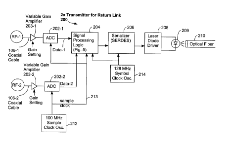
Referring to Fig. 4, there is shown a preferred embodiment of a dual RF
channel transmitter 200 of a digital return path link of the present
invention. In particular, the
transmitter 200 is preferably configured to receive two radio frequency (RF)
signals from two
separate coaxial cables 106-1, 106-2. Each RF signal is processed by a
variable gain
amplifier 203-1, 203-2 and digitized by a pair of analog to digital converters
(ADC) 202-1,
202-2. As will be discussed in more detail below, in some embodiments of the
present
invention the gain of each variable gain amplifier 203 is controlled via
commands received
from the head end of the system. These commands are received by a control
logic circuit 227
(shown in Fig. 5) which uses the commands to set the gain of the amplifiers
203, as well as to
set the mode of other components of the transmitter 200.
It should be understood by the reader that all clock rates, data structures
and
the like presented in this document are the values used in certain particular
embodiments of
the invention. Clock rates, data structures and the like may vary widely from
one
embodiment of the present invention to another, depending on the performance
requirement
of the embodiment as well as other factors.
The return path transmitter 200 further includes a sample clock oscillator 212
generating a 100 MHz sample clock signal 213. The oscillator 212 is preferably
located
directly next to one or both of the ADCs 202-1, 202-2. The sample clock
oscillator 212 is
used to digitize the incoming RF signals with very low fitter. Care is taken
to ensure that the
-9-
CA 02394231 2002-06-13
WO 01/43441 PCT/US00/33713
sample clock signal is not manipulated by any additional logic, because any
such logic may
increase fitter in the sample clock signal 213.
A single RF channel version of the transmitter 200 will be discussed below.
Furthermore, the preferred embodiments of the present invention can be
modified to receive
and process more than two RF signals. One such embodiment, herein called the
summer
embodiment or daisy-chain embodiment is discussed below.
In the preferred embodiment, each ADC 202-1, 202-2 is a twelve-bit A/D
converter from Analog Devices with a one volt differential input range,
clocked by the 100
MHz sample clock. Preferably, only ten bits of the twelve-bit output from the
ADCs 202-1,
202-2 are used. Of course the particular ADC used and the number of data bits
used will vary
from one implementation of the invention to the next. The outputs from ADCs
202-l, 202-2
are then passed through a signal-processing logic circuit 204 before being
presented to a
serializer-deserializer (SERDES) 206 (e.g., TLK-2500 from Texas Instruments).
The signal-processing logic circuit 204 processes the received RF signals and
outputs a sequence of data frames. In a preferred embodiment, each data frame
contains 80
bits of RF data; however the number of data bits per frame is a matter of
design choice and
thus may be different in alternate embodiments. The signal-processing logic
circuit 204 also
generates ancillary data words to be inserted between data frames and
generates a frame
control signal to indicate whether the output it is currently generating is
part of a data frame
or a part of the ancillary data stream. Subsequently, the output of the signal-
processing logic
circuit 204 is serialized by the SERDES 206, which also performs an 8b/lOb
data conversion
so as to produce a bit balanced data stream. The output of SERDES 206 is then
transmitted
by a digital transmitter 208, 209 down an optical fiber 210 as a digitally
modulated optical
signal.
A 128 MHz symbol clock signal, generated by a symbol clock 214, is
multiplied by the SERDES circuit 206 to produce a 2.56 Gb/s clock signal that
is used to
serially clock the bits from the SERDES circuit 206 to a laser diode driver
208.
Referring to Fig. S, there is shown a preferred embodiment of the signal
processing logic circuit 204, which is used in the transmitter 200 shown in
Fig. 4. A pair of
latches 220-1, 220-2 is provided to receive two digitized radio frequency (RF)
analog signals
from the ADCs 202-1, 202-2 (shown in Fig. 4). These two data signals are
hereinafter
referred to as the first and second data streams. The first data stream from
ADC 202-1 is
received by a first latch 220-l, and the second data stream from ADC 202-2 is
received by a
-10-
CA 02394231 2002-06-13
WO 01/43441 PCT/US00/33713
second latch 220-2. The first data stream, after it has been buffered and
converted into
frames of a predetermined size (e.g., 80 bits) is called the Frame A data, and
the second data
stream, after buffering and framing is called the Frame B data.
In a preferred embodiment the digitized data streams flowing through the
latches is dithered by adding on top of the data streams a set of "tone
signals" using a tone
generator and adder circuit 225-1, 225-2. In one embodiment, the tone
generator and adder
circuit 225 generates five tone signals, at frequencies of 100KHz, 200KHz,
300KHz, 400KHz
and SOOKHz and adds low amplitude versions of these tone signals to the RF
data streams.
The reason for adding the tone signals to the RF data streams is to prevent
the digital-to-
analog convert in the receiver from creating spurious noise in response to RF
data streams
that contain no data or almost no data. By adding the tone signals to the RF
data, where the
tone signals are at frequencies well below the frequency band containing data,
the generation
of this spurious noise is significantly reduced, typically by about 6 dB. In
the preferred
embodiments, the frequency band containing data is typically 5 MHz to 45 MHz
or 5 MHz to
1 S 65 MHz.
A pair of data-in multiplexors 221-1, 221-2 are provided to further process
the
latched data. Each of the data-in multiplexors 221-l, 221-2 is configured to
convert the 10
bit data streams from the ADCs into 16 bit data streams. Preferably, each
multiplexor 221
converts eight of the 10-bit input data words into five 16-bit output data
words that together
form a data frame.
Each of the data-in multiplexors 221-1, 221-2 also receives a set of test data
(preferably a digitized sinusoidal signal) generated by a test signal
generator 224. The test
data is used in testing the transmitter. The data-in multiplexors 221-1, 221-2
selectively
output either the digitized RF data streams or the test data in accordance
with a selection
(mode) signal generated by the control logic circuit 227. The data-in
multiplexors 221-1,
221-2 are also configured to generate an end of frame (EOF) flag signal to
indicate end of
each 80-bit data frame. More specifically, the data-in multiplexors 221-l, 221-
2 output a 1-
bit EOF flag for every 16-bit word output by the data-in multiplexors 221-1,
221-2. The EOF
flag is equal to a first value, such as 0, for the all the 16-bit words of
each data frame except
the last, and for that last 16-bit word the EOF flag is equal to a second
value, such as 1.
The 16 bit data words from the data-in multiplexors 221-1, 221-2 are then
forwarded to a pair of data memory devices 223-1, 223-2. In particular, the
data words
generated from the first data stream are forwarded to a data first memory
device 223-1 from
-11-
CA 02394231 2002-06-13
WO 01/43441 PCT/US00/33713
the first data-in multiplexor 221-1, and the data words generated from the
second data stream
are forwarded to a second data memory device 223-2 from the second data-in
multiplexor
221-2. In addition to the 16 bit data words, the first memory device 223-1
also stores the
EOF flag for each word. Alternately, the EOF flags for the data words of the
first data stream
S can be stored in a separate FIFO memory device.
Both memory devices 223-1, 223-2 store the received data words using the
100 MHz sample clock. However, data is written into the memory devices 223 on
only five
of every eight clock cycles of the 100 MHz sample clock because the data has
been
reformatted by the data-in multiplexors 221 from 10 bit words into 16 bit
words. Reads from
the memory devices 223 are performed using the 128 MHz symbol clock. The data
memory
devices 223-1, 223-2 are first-in-first-out (FIFO) memory devices, preferably
implemented
using one or more dual ported RAM's. The writing and reading of data from the
memory
devices 223 is controlled by a control logic circuit 227, which is implemented
using state
machine logic.
It is noted that reading 16-bit words from the memory devices 223 and 229 at
128 MHz results in a data being sent to the SERDES 206 at a rate of 2.048
Gb/s. After the
SERDES converts each 16 bit word into a 20 bit word, the resulting data rate
is 2.56 Gb/s.
The signal-processing logic 204 further includes a set of sensors 226 for
monitoring temperature, supply voltage or other voltages, and other parameters
of the
transmitter 200. The sensor generated values are read by a processor 228,
which also
includes an internal memory device 230 for storing transmitter identifying
information such
as serial numbers, model numbers, software and hardware revisions, date of
manufacture and
the like of the transmitter 200. The processor periodically forwards the
sensor generated
values as the transmitter identifying information, herein collectively called
maintenance data,
to a FIFO memory device 229. In a preferred embodiment forwards the
maintenance data to
the memory device 229 once every 40 ms.
The control logic circuit 227 of the signal processing logic 204 is configured
to generate read and write addresses for the various memory devices. With
respect to the data
memory devices 223-1, 223-2, the control logic circuit generates write address
during five of
every eight cycles of the 100 MHz sample clock and generates read addresses at
128 MHz.
The control logic circuit 227 alternates between reading data from first and
second memory
devices 223, alternating between reading one data frame (i.e., five 16-bit
words) from one and
one data frame from the other. In addition, when certain criteria are met, the
control logic
-12-
CA 02394231 2002-06-13
WO 01/43441 PCT/US00/33713
circuit 227 reads maintenance data from the third memory device 229 (i.e.,
sends the
maintenance data to multiplexor 231).
Data is read from the memory devices 223 at a rate that is faster than the
combined rate at which data is stored in the two memory devices 223 so that
ancillary data
from the third memory device can be inserted between data frames without
"falling behind"
the first and second data streams that are being stored in the two memory
devices 223. When
there is no maintenance data in memory device 229, or more particularly when
there is not
yet a complete set of maintenance data ready for transmission, padding words
(preferably
idles) are inserted between frames at certain times.
When ancillary data words are to be inserted between data frames, a counter
located inside the control logic circuit 227 that generates the read addresses
is stopped,
thereby causing the data memory devices 223-1, 223-2 to keep on outputting the
same data
word. The control logic 227 also generates a SERDES control signal that sets
the mode of
operation of the SERDES 206 (Fig. 4). In particular, the SERDES is instructed
by the control
logic circuit 227 to either (A) perform a 16b to 20b conversion on a data
word, (B) output an
idle word, or (C) output a carrier word.
The control logic circuit 227 and multiplexor 231 are configured to monitor a
fullness level of the RF data memory device 223-1 and maintenance data memory
229, output
data stored in the RF data memory devices 223-1, 223-2 in a first mode when
the fullness
level of memory device 223-1 is more than a predefined threshold level, and to
output data
stored in the RF data memory devices 223-1, 223-2 and the maintenance (i.e.,
non-RF) data
stored in the memory device 229 in a second interleaved mode when the fullness
level of the
RF data memory device 223-1 is less than the predefined threshold level.
Figs. 6A-6C illustrates three different modes for inserting the ancillary data
words between the data frames. In these figures, time flows from left to
right. This means
that the data frame on the left side is output earlier in time than the data
frame on the right
side. Hence, each sequence starts from an A data frame. Here, an A data frame
is a data
frame generated from the first data stream, and a B data frame is a data frame
generated from
the second data stream.
Refernng to Fig. 6A, in a first mode during which no ancillary data streams
are inserted between the data frames, a sequence of A and B data frames are
generated. In
other words, a data frame (of five words) from the first data stream is
followed by a data
frame from the second data stream which in turn is followed by the next data
frame from the
-13-
CA 02394231 2002-06-13
WO 01/43441 PCT/US00/33713
first data stream and so on. The control logic circuit 227 operates in this
mode when the
amount of data stored in the data memory devices 223-1, 223-2 is above a
predefined
threshold fullness level, which requires the stored data to be read out as
quickly as possible.
More specifically, every time the write address generated by the control logic
circuit 227 cycles back to its starting value (e.g., zero), the read address
generated by the
control logic circuit 227 is compared with a predefined value, such as read
address value at
the middle of the memory devices and a "fullness" signal is generated based on
that
comparison. When the write address (also called the write pointer) is at its
starting value and
the read address is at the middle value, the memory devices are half full.
When the read
address is less than the middle value, the memory devices are less than half
full and the
fullness signal is set to a first value (e.g., "false") and when the read
address is greater than or
equal to the middle value, the memory devices are at least half full and the
fullness value is
set to a second value (e.g., "true). The value of the fullness signal remains
unchanged until
the write address recycles back to its starting value, at which time the
fullness signal is re-
evaluated. When the fullness signal generated by the control logic circuit is
equal to the
second value (true), the transmitter operates in the mode shown in Fig. 6A,
sending only RF
data frames and no ancillary data. However, since the data transmit rate is
greater than the
data receive rate, by about 2.5% in the preferred embodiment, the fullness
value will often be
equal to the first value, indicating that either idles or ancillary data can
be inserted into the
output data stream.
Refernng to Fig. 6B, during a second mode, four idle words are inserted as the
ancillary data between a B frame and an A frame. More specifically, a data
frame from the
second data stream is followed by four idle words which is followed by a data
frame from the
first data stream. This in turn is followed by a data frame from the second
data stream and so
on. The control logic circuit 227 operates in this mode when the amount of
data stored in the
memory devices is below the threshold fullness level (i.e., the fullness
signal has a value of
"false"), but there is no maintenance data that is ready to be transmitted in
the memory device
229. The control logic circuit 227 is synchronized with the boundaries of the
output data
frames by the EOF framing bit that it receives whenever the last word of an A
frame is
output. Using the EOF framing bit, the current fullness value, and a signal
indicating whether
there is maintenance data that is ready to be transmitted from the memory
device 229, the
control logic will insert four idles after the end of the next B frame when
the fullness value
-14-
CA 02394231 2002-06-13
WO 01/43441 PCT/US00/33713
has a value indicating the memory devices are below the threshold fullness
level and there is
no maintenance data that is ready to be transmitted in the memory device 229.
Referring to Fig. 6C, during a third mode, between a B frame and an A frame
four words are inserted. In particular, the four words, forming the ancillary
data includes one
idle word, one Garner word and two maintenance data words. The carrier word is
used to
indicate that the two maintenance data words are transmitted instead of the
last two idle
words. The control logic circuit 227 operates in this mode when the amount of
RF data
stored in the memory devices is below the threshold level and there is
maintenance data in
memory device 229 that is ready to be transmitted. If, for example, the amount
of
maintenance data to be transmitted is 100 words, approximately 24 words of
this data will be
transmitted each time the memory devices 223 are determined to be below the
threshold
level. These 24 words of maintenance data are transmitted, two words at a
time, after each of
twelve successive B frames, after which the fullness of the memory devices 223
will be re-
evaluated. At the gigabit per second data rates used in the system, and the
generation of a
new packet of maintenance data only once every 40 ms (occupying a bandwidth of
approximately 100 Kb/s, including the idle and carrier overhead words and
8b/lOb encoding
overhead), the maintenance data occupies only a very small fraction of the 60
Mb/s
bandwidth available in the auxiliary data "channel." (Of the 60 Mb/s bandwidth
of the
auxiliary data channel, 50% is used by idle and carrier marks to denote the
presence of data in
the channel, and 20% of the remaining bandwidth is occupied by the 8b/1 Ob
encoding,
resulting in a true raw auxiliary data bandwidth of approximately 24 Mb/s.
This 24 Mb/s of
available bandwidth is still very, very large compared to the 40 Kb/s raw data
rate used for
maintenance data transmission in the preferred embodiment.)
Referring to Fig. 5, the data frames generated from the first and second data
streams along with the maintenance data are sent to a data-out multiplexor
231. The
operations of the data-out multiplexor 231 are controlled by the control logic
circuit 227. In
summary (as will be explained in more detail below), the data-out multiplexor
231 operates
in one of the three modes discussed above in connection with FIGS. 6A-C.
In addition, the control logic circuit 227 sends control signals to the SERDES
206 (Fig. 4) to control the transmission of data from the data memory devices
223-l, 223-2
and idle words.
As discussed above, the output of the data-out multiplexor 231 is prepared for
the serializer/deserializer (SERDES) circuit 206, a link serializer chip which
has a sixteen-bit
-15-
CA 02394231 2002-06-13
WO 01/43441 PCT/US00/33713
wide input. Each sixteen-bit word is converted by the SERDES circuit 206 into
a twenty-bit
symbol. Only the serializer function of the SERDES circuit 206 is used in
transmitter 200,
while the deserializer function is used in the receiver 250. The SERDES
circuit 206 maps all
possible eight-bit symbols into ten-bit symbols that are "balanced" with
respect to 1 and 0
bits, and which provide sufficient data transitions for accurate clock and
data recovery.
Further, the SERDES circuit 206 maps two eight-bit words at a time, and thus
converts
sixteen-bits of data at a time into twenty-bit symbols. This mapping, called
link encoding or
8B/lOB encoding, adds twenty-five percent overhead to the transmitted data
stream.
Therefore if data is submitted to the link at a rate of 2.00 Gb/s, the link
must transmit data at a
rate of at least 2.5 Gb/s. In the preferred embodiment, the optical link
operates at 2.56 Gb/s.
The extra bandwidth is used by the link to transport the ancillary data.
Serial data from the
serializer circuit 206 is driven into a fiber optic transmitter 208, 209 that
converts electrical 1
and 0 bits into optical l and 0 bits. This fiber optic transmitter includes a
laser diode driver
208 and a laser diode 209. This device modulates the light generated by the
laser 209 and
also keeps it stable over temperature and changing supply voltages.
Return Path Single RF Signal Transmitter
A single RF data channel RF signal transmitter 200-1X is shown in Figs. 7 and
8. Since the operation of this version of the RF signal transmitter is almost
identical to that of
the return path dual RF signal transmitter described above with respect to
Figs. 4, 5 and 6,
only the aspects of this transmitter 200-1X that differ from the dual channel
transmitter 200
will be described here.
First, of course, the single RF data channel transmitter 200-1X uses only one
input amplifier 203, ADC 202, data latch 220 and tone adder 225. Since the
single channel
transmitter 200-1X has only one channel of RF data, with a raw data rate of
1.0 Gb/s, the
symbol clock (produced by symbol clock generator 214-1X) can use a rate as low
as 64 MHz,
which is half the speed of the symbol clock of the dual channel transmitter.
In one
embodiment, the single channel transmitter 200-1X uses a symbol clock rate of
80 MHz
because that is the minimum clock rate useable with a preferred SERDES 206
circuit. In this
embodiment, additional bandwidth is available for use in the auxiliary
channel. For
convenience, the single channel transmitter will be described with a 64 MHz
symbol clock,
but it is to be understood that clock rates above 64 MHz would work equally
well.
-16-
CA 02394231 2002-06-13
WO 01/43441 PCT/US00/33713
Referring to Fig. 8, the control logic circuit 227-1X uses the A frame EOF
signal slightly differently than in the dual channel version. In particular,
if the data memory
device fullness signal have been evaluated to be "false," indicating the
memory device 223 is
less than the threshold level of fullness, and there is maintenance data ready
for transmission
in the maintenance data memory 229, then an I C M M sequence of idle, channel
and
maintenance data words is inserted after the A frame so as to interleave
maintenance data
with the A frame data. If there isn't maintenance data ready for transmission
in the
maintenance data memory 229, and the fullness signal is "false," then four
idle words are
inserted after the A frame. When the fullness signal is "true," A frames are
transmitted
without interruption by idles or maintenance data.
Return Path Receiver
The receiver 250 at the receive end of the link receives the digitally
modulated
light, processes it with a sequence of digital signal-processing circuits
which prepare the data
and then passes it onto a pair of digital to analog (D/A) converters 270-1,
270-2. The output
of the D/A converters 270-l, 270-2 are "regenerated RF signals" that closely
match both the
frequency domain and time domain characteristics of the RF signals on coaxial
cables 106-l,
106-2, respectively. The dual channel version of the receiver 250 will be
described first; the
single channel version of the receiver will then be described in terms of the
differences
between dual and single channel versions.
Refernng to Figs. 9 and 10, the receiver 250 at the receive end of the optical
fiber 210 includes a fiber receiver 252, 254 that changes the optical 1 and 0
bits transmitted
over the optical fiber 210 back into the appropriate electrical 1 and 0 bits.
This serial bit
stream is driven into a deserializer circuit 258 of a serializer/deserializer
(SERDES) circuit
256 (e.g., TLK-2500). The SERDES circuit 256 also includes a clock recovery
circuit 260
that recovers the 2.56 GHz bit clock and the 128 MHz symbol clock from the
incoming data.
The deserializer 258 converts the received data from twenty-bit words into
sixteen-bit data
words using either standard or proprietary l Ob/8b or 20b/16b decoding. The
sixteen-bit data
words are in turn clocked, using the recovered symbol clock, into a receiver
signal processing
logic circuit 262. The deserializer 258 generates a set of flag signals in
addition to decoded
data values. The flag signals indicate whether the current symbol is a data
word, idle word,
-17-
CA 02394231 2002-06-13
WO 01/43441 PCT/US00/33713
or carrier word. Maintenance data words are identified by the signal
processing logic 262 as
the two data words following an idle word and carrier word.
The receiver signal processing logic 262 is implemented in the preferred
embodiment using a field programmable gate array (FPGA), a QL4016 from
QuickLogic,
which includes a pair of receiver data memory devices 280-1, 280-2 in the dual
channel
version of the receiver, and one such data memory device in the single channel
version. The
memory devices 280-1, 280-2 are preferably FIFO memory buffers implemented by
one or
more asynchronous dual ported RAM's (random access memory's).
Referring to Figs. 10 and 1 l, the receiver's signal processing unit 262
includes
a demultiplexor 279 which receives the deserialized data and the flag signals
from the
deserializer 258. The demultiplexor 279 is configured to send data words from
the A frames
to memory device 280-1, and data words from B frames to memory device 280-2
and
maintenance data to a memory device for maintenance data 281. Each transition
from a data
word to an idle word is used to reset a state machine in the demultiplexor to
a starting (Idle 1)
state, which in turn allows the multiplexor 279 to accurately generate an end
of frame bit for
each RF data word. Idles and Garner words are not written into any of the
memory devices.
The demultiplexor 279 is also configured to generate appropriate write enables
signals,
transmission error bit and end of frame signals. A transmission error bit and
end of frame bit
are generated for each data word and are forwarded to memory devices 280 for
storage along
with the data words. In an alternate embodiment, the transmission error bit
and end of frame
bit for each data word can be stored in a parallel memory device.
Fig. 11 shows a simplified state diagram for the receiver demultiplexor 279.
This diagram shows the main states, but does not show all error states and
furthermore
clumps together certain groups of states such as the individual data word
states. Thus, the
Maint Data state handles the storage of two data words into the maintenance
data memory
device 281. More importantly, the Frame A state handles a sequence of five
data words,
storing four in memory device 280-1 with EOF set equal to 0 and storing the
last data word in
memory device 280-1 with EOF set equal to 1. The Frame B state similarly
handles a
sequence of five data words, storing four in memory device 280-2 with EOF set
equal to 0
and storing the last data word in memory device 280-2 with EOF set equal to 1.
Each
transition from a data word to an idle word resets the state machine back to
the Idle 1 state,
regardless of the current state of the state machine (i.e., this happens not
only when in the
Frame B state). As a result, if the receiver becomes desynchronized with the
transmitter, for
-18-
CA 02394231 2002-06-13
WO 01/43441 PCT/US00/33713
instance if there is a transmission error that causes the receiver to loose
track of where it is in
the transmitted data sequence, the data word to idle word transition is used
to reset the
demultiplexor back to a well defined state.
Referring again to Fig. 10, a receiver control logic circuit 283 generates
read
and write addresses for the various memory devices located in the receiver
signal processing
unit 262. With respect to the data memory devices 280-1, 280-2, the control
logic circuit 283
generates write address at 128 MHz (for writing 16 bit data words into memory
devices 280-
1, 280-2 and 281) and the read addresses at 100 MHz (for reading 16-bit data
words out of
each of the memory devices 280-1 and 280-2 in parallel). However, data is read
from the
memory devices 280-1 and 280-2 on only five of every eight clock cycles of the
100 MHz
sample clock so that one 80-bit data frame is transferred from each memory
device 280 once
every eight cycles of the 100 MHz sample clock.
A clock speed adjusting circuit 284 determines whether an excessive amount
of data is stored in the data memory devices 280-1, 280-2 by monitoring the
read and write
1 S addresses. In particular, each time the write address generated by the
control logic 283 wraps
around to a starting value, the fullness of the memory devices 280 is
determined by
comparing the current read address with a predefined threshold. When the read
address
indicates that the fullness of the memory devices 280 is above a threshold
fullness level (e.g.,
a half), the clock speed adjusting circuit 284 adjusts a clock adjusting
signal 266 so as to
reduce the memory read clock rate (which has a nominal rate of 100 MHz), and
when the
memory devices 280 are at or above the threshold fullness level the clock
speed adjusting
circuit 284 adjusts the clock adjusting signal 266 so as to increase the
memory read clock
rate. The clock speed adjusting circuit 284 preferably makes this
determination each time the
write address wraps around to a starting value, and then adjusts the clock
adjusting signal 266
accordingly.
A 100 MHz VCXO (voltage controlled crystal oscillator) 264 is used to
generate a sample clock signal 265, also called the read clock, that is locked
to the 100 MHz
sample clock 213 of the transmitter 200. The VCXO 264 is tuned to have a
center frequency
of 100 MHz, and to respond to the clock adjusting signal 266 by preferably
varying its
frequency by plus or minus 100 parts per million (i.e., from a low of 99.99
MHz to a high of
100.01 MHZ).
If the rate of the sample clock 265 in the receiver 250 is faster than the
rate of
the sample clock 213 in the transmitter 200, then the receiver memory devices
280-l, 280-2
-19-
CA 02394231 2002-06-13
WO 01/43441 PCT/US00/33713
will become less than half full, at first intermittently and then
consistently. When the clock
speed adjusting circuit 284 determines that the memory devices 280-1, 280-2
are less than
half full (or more generally, less than a threshold level of fullness), the
clock adjusting signal
266 is adjusted and applied to a speed adjust pin of the VCXO 264 to slow its
100 MHz clock
S rate down by a small amount. The rate of the sample clock 265 generated by
the VCXO 264
is adjusted until it is roughly in balance with the sample clock 213 of the
transmitter 200.
While actual balance between the sample clocks 265, 212 of the receiver 250
and transmitter 200 may never occur, the clock tracking circuitry of the clock
speed adjusting
circuit 284 permits the return path link system to dynamically achieve full
frequency tracking
and locking between the sending and receiving ends of the link.
The use of the VCXO 264, which runs off a local crystal, to generate the
receiver's sample clock 265 enables the generation of a very low fitter sample
clock while
still allowing the use of a correcting voltage to speed up or slow down the
sample clock.
The receiver signal processing logic 262 further includes sensors 286 that
monitor temperature, voltages and other parameters of the receiver 250. A
processor 282
includes an internal memory device 288 that stores serial numbers, model
numbers, software
and hardware revisions, date of manufacture and the like of the receiver 250.
The processor
282 periodically stores receiver maintenance data, including sensor data
received from the
sensors 286 and the receiver identification data stored in the processor's
internal memory
288, in memory device 281. Thus memory device 281 stores both transmitter
maintenance
data packets and receiver maintenance data packets. The control logic circuit
283 is
configured to read out the maintenance data from both the transmitter and
receiver stored in
the memory device 281 and send them serially out through a communication
interface 287,
such as an RS-232 interface, to either a main controller of the receiver 250
or to a host
computer. The device receiving the maintenance data can store it and/or
analyze the
maintenance data so as to determine whether the transmitter and receiver are
operating
properly.
The receiver signal processing logic 262 also includes a pair of deblocking
multiplexors 285-l, 285-2. The deblocking multiplexors are configured to
receive the data
read out from the memory devices 280-1, 280-2 along with associated control
signals. The
deblocking multiplexors 285-l, 285-2 are configured to convert each 80 bit
data frame from a
set of five 16-bit words into eight 10-bit words; this data format conversion
is herein called
the deblocking function. In addition, the deblocking multiplexors 285-l, 285-2
use the end of
-20-
CA 02394231 2002-06-13
WO 01/43441 PCT/US00/33713
frame flag signal to reset the deblocking function in case it ever gets out of
sync. This gives
the receiver 250 a very substantial error recovery process. Any deblocking
error will
automatically be fixed when the next end of frame is received. If for any
reason the
deblocking circuitry gets "out of synch" with the data stream, the circuitry
automatically
recovers within one frame length of 80 bits (five 16-bit words); for instance,
upon receiving
an EOF signal that is not in the fifth 16-bit word of the current data frame,
a deblocking
multiplexor 285 may discard the data in the current frame and then restart its
processing by
treating the next data word from memory device 280 as the first 16-bit word of
a next data
frame.
Moreover, if a data word read out of the memory devices 280-1, 280-2 has the
transmission error bit set in, the deblocking multiplexors 285-l, 285-2
substitute the last
previous good value that was read out of the memory devices 280-l, 280-2 in
place of the bad
received value. For most cases, this will be the same or close to the actual
data transmitted in
error. This gives the receiver 250 the opportunity to digitally filter out a
single transmission
error from the data stream.
The deblocking multiplexors 285-1, 285-2 may also operate in a test mode,
sending test data generated by a test generator circuit 289 in place of the RF
sample data from
memory devices 280-1, 280-2.
The single channel version of the return path receiver is essentially the same
as
that shown in Figs. 9 and 10, except as follows. Only one memory device 280
and one
deblocking multiplexor 285 is needed. Thus, received RF data is sent by the
demultiplexor
279 only to the one memory device 280 and maintenance data is sent to memory
device 281.
In addition, the sample clock of the single channel receiver operates at 64
MHz instead of 128
MHz.
Discussion of CATV Digital Return Path Clock Generation and Management
As discussed above, digital CATV return path systems require the A/D and
D/A sampling clocks to be at the same frequency, with very low fitter.
Furthermore, in prior
art systems, the frequency of the A/D clock must be transported over the
communications
link with the sampled data to reconstruct the signal. Jitter on either
sampling clock results in
noise in the recovered analog signal.
-21
CA 02394231 2002-06-13
WO 01/43441 PCT/US00/33713
In the present invention, at the transmitter 200 shown in Fig. 4, a low noise
oscillator 212 is used to generate the sample clock that is used to clock data
from the A/D
converter 202 into the FIFO buffers 223-1, 223-2. A separate oscillator 214 is
used to
generate the symbol clock for the transmitter. In order for the frequency of
the symbol clock
generator 214 to be independent of the sample clock frequency, the
transmission rate over the
communications link must be higher than the data rate generated by the A/D
converters 202-
1, 202-2. The transmitter's signal processing logic 204 sends data from the
FIFO buffers
223-1, 223-2 over the optical fiber 210 when there is sufficient data in the
FIFO buffers 223-
1, 223-2, and otherwise the data sent over the optical fiber 210 is padded
with other
characters.
The receiver 250 receives data from the communications link 210 and recovers
the symbol clock signal 274. The receiver 250 recognizes which received
symbols are data
and which are pad characters. The data symbols that are RF data samples are
placed in the
receive FIFO buffers 280-1, 280-2 (Fig. 10) using the symbol clock signal 274.
RF data
samples are sent from the FIFO buffers 280-1, 280-2 to the D/A converters 270-
1, 270-2 at
the sample clock rate. The regenerated RF signals produced by the D/A
converters 270-1,
270-2 are processed by a CMTS (cable modem termination system) 134, which
processes the
RF signals so as to determine the subscriber originated messages encoded in
those RF
signals. Depending on the configuration of the CMTS 134, the two regenerated
RF signals
may be summed on an input port of the CMTS 134, or the two regenerated RF
signals may be
directed to different input ports of the CMTS 134.
In an alternate embodiment shown in Fig. 9A, the digital RF data samples in
FIFO buffers 280-1 and 280-2 are mathematically summed by a summer 267 and the
resulting sum is sent to a single D/A converter 270 at the sample clock rate.
The D/A
converter 270 generates an analog, regenerated RF signal that is equal to the
sum of the two
RF signals that were sampled at the two subtrees. From another viewpoint, the
analog signal
comprises regenerated versions of the first and second RF signals superimposed
on each
other. The regenerated RF signal is sent to the CMTS 134 for processing.
The sample clock 265 is generated by the VCXO 264. The VCXO's 264
frequency is adjusted slowly over a small range to keep the rate of data taken
from the FIFO
buffers 280-1, 280-2 the same as the rate data is placed into the FIFO buffers
280-l, 280-2.
Control of the VCXO's 264 frequency is accomplished based on the amount of
data in the
FIFO buffers 280-1, 280-2. If the FIFO buffers 280-1, 280-2 are more than half
full (or any
-22-
CA 02394231 2002-06-13
WO 01/43441 PCT/US00/33713
other appropriate threshold level), the VCXO's 264 frequency is increased,
taking data out
faster. If the FIFO buffers 280-1, 280-2 are less than half full, the VCXO's
264 frequency is
decreased, taking data out slower.
Accordingly, the present invention has lower receiver sample clock time fitter
than the prior art systems depicted in Figs. 2 and 3 because the receiver's
sample clock is not
contaminated by noise associated with recovery of the symbol clock.
More specifically, in the prior art systems, the recovered clocks derived from
a
multiplied clock at the transmitter end 150 (Fig. 2) of the link typically
will have fitter of
more than 10-20% of the bit cell time. When the link rate is 1.25 Gb/s, (with
a bit cell time
of 800 ps) it is not uncommon for the received sample clock to have fitter of
100 ps or more.
When a sample clock with that level of fitter is used to clock the D/A
converter of a receiver,
the fidelity of the recovered RF signal will not be able to exceed that of an
ideal 8-bit A/D
and D/A conversion system.
However, the return links of CATV systems generally require close to a full
10 bits of data in order to match the performance of traditional analog based
laser return path
links. The frequency locking method of the present invention, including the
use of VCXO in
the receiver 250, allows the receiver's sample clock to be generated with
fitter levels of 20-30
ps for signals between 5 and 50 MHz.
The use of a digital return path in accordance with the present invention has
many benefits. For instance, the length of the return path link can be very
long without
hurting performance, because digital link performance generally does not vary
with link
distance. Digital fiber optic links can be designed so that there is
sufficient SNR for the link
to operate "error free" for all practical purposes. Link error rates of less
than 10-'S are not
uncommon. Because of this, the return path link system does not show
diminished
performance from distances as short as 1 meter to those as long as 30 km of
fiber or more.
Link performance generally does not vary with poor splices, connectors,
device temperature or normal voltage excursions. Again, the characteristics of
the link with
these changes can be measured, but even with these changes, while they do
affect analog
measurements, the SNR can be generally kept in the range where error free
digital
performance is still possible. Therefore, the return path RF link of the
present invention
operates with a constant SNR over the component variations.
Further, since digital return paths exhibit similar performance to analog
return
paths under "perfect conditions", digital return paths are able to provide
greater immunity to
-23-
CA 02394231 2002-06-13
WO 01/43441 PCT/US00/33713
ingress because margin, normally allocated to link degradations such as
length, splices and
temperature variations, can now be allocated to handling ingress, enabling the
system to
operate in spite of ingress that would normally drive a return path link
system into clipping.
Combining Return Path Data from Multiple Subtrees
Figs. 12 and 13 depict an embodiment of the present invention in which the
return path data streams from two or more subtrees 300 are received over
optical fibers 210,
combined at a hub 330 using time division multiplexing (TDM) and then
transmitted over the
optical fiber 360. The transmitters for each subtree of the system are the
same as described
above, except that in this embodiment the sample clock for the transmitter
(for clocking the
ADC's 202) is generated by a separate low noise, precision VCXO (voltage
controlled crystal
oscillator) 212-A. Furthermore, in order to enable the data streams from the
various subtrees
to be easily combined, the clock rates of the VCXO's 212-A in all the subtrees
are controlled
by a pilot tone by oscillator lock logic 308 that is included in the
transmitter of each subtree.
It is noted that while the rates of all the VCXO's 212-A are forced to the
same value, the
phases of these clocks are not (and do not need to be) coordinated.
In an exemplary embodiment, the pilot tone is a clock that runs at
approximately 40% of a predefined target sample clock rate. For instance, the
pilot tone may
be a 40 MHz clock signal when the target sample clock rate is 100 MHz. The
oscillator lock
logic 308 for each subtree 300 receives the locally generated sample clock and
generates a
correction voltage that ensures that the sample clock rate is precisely equal
to 2.5 times the
pilot clock rate. Locking of the VCXO 212-A to the pilot tone is accomplished
by counting
pulses from each and generating a suitable correction voltage (using pulse
width modulation
and low pass filtering) that is applied to the VCXO. In other embodiments,
other sampling
clock rates, pilot tone clock rates and sample to pilot clock rate ratios can
be used.
Fig. 12 shows apparatus for distributing the pilot tone to the subtrees of a
CATV system. At the head end system 310, forward link signals are produced by
television
signal feeds 312, digital signal feeds 314 (e.g., data from an Internet
service provider for
viewing by subscribers using browsers) and a pilot tone generator 316. The
pilot tone
produced by generator 316 is preferably a sinusoidal signal that is added to
the television and
other signals transmitted over the forward path of the CATV system by a head
end transmitter
318. At each subtree 300, a notch filter 304 is used to separate out the pilot
tone from the
-24-
CA 02394231 2002-06-13
WO 01/43441 PCT/US00/33713
other signals on the forward path, and an amplifier 306 is used to convert the
extracted
sinusoidal pilot tone into a pilot clock signal. The pilot clock signal is
received by the
oscillator lock logic 308 of the subtree's transmitter, the operation of which
is described
above.
As shown in Fig. 13, the return path transmitter apparatus, herein called a
hub
330, receives data from two or more subtrees via optical fibers 210. The hub
330 includes a
digital receiver 332 for converting the signals from each subtree into
electronically stored or
buffered data frames which then forward the data frames to a time division
multiplexor or
wavelength division multiplexor 334. The hub 330 may also receive data from
another
service or source 314. For instance, the other source 314 may be a system that
generates test
patterns to enable the head end system to detect data transmission errors.
Signal processing logic in the multiplexor 334 preferably includes a separate
FIFO buffer for storing data from each subtree, as well as a FIFO for storing
data from the
other sources 314. The FIFO buffers for all the subtrees will always, at the
beginning of each
1 S frame transmission period, have the same level of fullness. Whenever the
FIFO buffers for
the subtrees are more than half full, a frame of data from each subtree FIFO
is transmitted
over the return path link. When time division multiplexing is used, the
combined data signal
is transmitted using a single laser diode driver 336 and laser diode 338. When
wavelength
division multiplexing is used, multiple laser diode drivers and laser diodes
are used.
Whenever the FIFO buffers for the subtrees are less than half full, one or
more
frames of data from the FIFO for the other service 314 is transmitted over the
return path
link, and if there is insufficient data in the FIFO for the other service 314,
the frames
allocated to the other service are filled with pad symbols. The bandwidth
available for data
from the other service 314 depends on the difference between the output
transmission rate of
the hub and the combined input data rates of the data streams from the
subtrees coupled to the
hub.
In this embodiment, all the subtree return path transmitters have essentially
the
same sampling clock frequency. This enables the system to have coherence
between the
return path signals as they are collected in intermediate points throughout
the system, which
in turn enables low cost aggregation of the return path signals.
In TDM implementations where the sample clocks of the subtrees are not
controlled by a pilot tone, and thus will vary somewhat from each other, the
signal process
logic of the multiplexor 334 adds and drops pad characters, as necessary, from
the incoming
- 25 -
CA 02394231 2002-06-13
WO 01/43441 PCT/US00/33713
data streams to make up for differences between the clock rates of the
received data streams
and the clock rate of the hub's symbol transmission clock. As long as the
bandwidth
occupied by pad characters in each data stream exceeds the worst case mismatch
in clock
rates between the hub's outgoing symbol clock and the clock rates of the
incoming data
streams, no data will ever be lost using time division multiplexing. For
instance, the signal
processing logic of the multiplexor 334 may insert pad symbols in place a data
frame for a
particular subtree when the RF data FIFO buffers for the other subtrees
contain sufficient data
for transmission of a next data frame but the FIFO buffer for the particular
subtree does not.
As indicated above, a hub may use a wavelength division multiplexor (WDM).
In one embodiment, the WDM is a coarse wavelength division multiplexor that
transmits two
or more data streams on two or more respective optical wavelengths. Using
"coarse"
wavelength division multiplexing means that the optical wavelengths of the two
optical
signals are at least 10 nm apart (and preferably at least 20 nm apart) from
each other. In a
preferred embodiment, each optical fiber 360 carnes a first 2.56 Gb/s data
stream at 1310 nm,
and a second 2.56 Gb/s data stream at 1550 nm.
Aggregation of return path data streams using the node and hub subsystems
shown in Figs. 4, 7 and 13 allows digital return streams to be built up from
tributaries and
then broken back down at the head end again. Moreover, each individual return
can still have
its master A/D clock recovered at the head end using the VCXO and FIFO method
described
above.
Second Method of Traffic Aggregation
In prior art systems, return paths are normally aggregated using analog RF
combination techniques, but this causes the link noise to increase without any
increase in
signal. Digital aggregation using time division multiplexing, as described
above, allows
simultaneous transport of multiple data streams over a single fiber without
signal
degradation.
Synchronizing of all of the return path clocks to a single frequency reference
allows simpler digital aggregation of multiple streams because the data from
each stream is
coherent with the others. For example, two return path data streams can be
combined by
simple addition of the data. This is the same as performing an RF combination,
but it does
not require that the signals be taken from the digital domain back to analog.
This method of
-26-
CA 02394231 2002-06-13
WO 01/43441 PCT/US00/33713
combination may be performed at a node where two or more subtrees meet, at an
intermediate
point in the CATV system such as a Hub, or can be performed at the head end
before the
signals are processed by a CMTS at the head end system. In all cases, the
methods are the
same and the ability to perform this function digitally means that no
additional losses in
S signal integrity beyond what would happen from theoretical arguments (i. e.
normal signal to
noise degradation) will occur. Because it is possible to design the CATV
system using
digital returns with SNR levels that cannot be obtained using analog fiber
optic methods, it is
therefore possible to start with signals that are so clean that significant
levels of digital
combining can be performed. This enables the system meet other objectives,
such as cost
reduction and signal grooming under changing system loads.
It is noted that the return link system shown in Figs. 2 and 3 requires
synthesizers in both the transmitter and the receiver, while the present
invention uses a
synthesizer only in the receiver, thereby lower the cost and increasing the
reliability of the
return path link.
Daisy Chain Version of Return Link System
Using Summing RF Transmitters and Large Bandwidth Non-RF Data Channel
Now that a complete description has been provided of a few embodiments of
the present invention, a "daisy chain" embodiment shall be presented, as well
as a number of
alternate embodiments of the daisy chain embodiment. Whenever the daisy chain
embodiment uses components whose function is the same as in previous
embodiments, those
components are labeled with the same reference numbers in the diagrams and
explanations of
the daisy chain embodiment(s), and furthermore the function and operation of
such
components shall be explained only to the extent necessary to understand their
function and
operation in the daisy chain embodiment(s).
Fig. 14 shows a CATV digital return path link system 400 in which a plurality
of the subtree return link transmitters 402 are connected in a daisy chain,
and which
furthermore provide a set of large bandwidth digital channels in addition to
providing a
digital return path link for RF data. More specifically, in the embodiment
shown the return
links of up to eight subtrees of the CATV system are serviced by the "summing
RF
transmitters" 402, although the number of subtree RF transmitters may be more
or less in
other embodiments. Each summing RF transmitter 402 receives a data stream from
a
-27-
CA 02394231 2002-06-13
WO 01/43441 PCT/US00/33713
previous node as well as the RF data signal from a local subtree. The summing
RF
transmitter 402 sums the RF data in the received data stream with the RF data
from the local
subtree J (where J is an index that identifies the local subtree), converts
the resulting data
stream into an optical digital signal, and forwards the resulting optical
digital signal over an
optical fiber 404-J to a next node of the system. The first summing RF
transmitter 402 in the
daisy chain receives a data stream over an optical fiber 404-0 (or alternately
over the main
optical fiber and cable forward path) from a set of routers 406 at the head
end of the system.
This data stream will be described in more detail below. The last summing RF
transmitter
402 in the daisy chain sends its output data stream to a hub 408 at the head
end of the system.
By summing the RF data from multiple subtrees, the RF signals are
superimposed on each other, and the resulting data stream represents the sum
(also called the
superposition) of these RF signals.
Each summing RF transmitter 402, in addition to sending RF data to the head
end system, also receives, forwards and routes a set of large bandwidth data
channels. In the
exemplary embodiment, each summing RF transmitter 402 has a separate 100 MHz
data
channel, for instance implemented as an Ethernet channel. The data stream
received by each
RF transmitter includes a 100 MHz data channel for each subtree. The RF
transmitter routes
the data in its data channel to a router or other device (not shown) at the
local node, and also
inserts into this data channel a stream of data stream. Thus, the received
data in the channel
for the local node is "dropped" onto a local bus, and data provided by the
local node is
"added" to the channel. In most embodiments, it is expected that the non-RF
data stream for
each subtree will be a full duplex data channel having a data rate of at least
S Mb/s.
Alternately, the non-RF data stream may be implemented as a half duplex data
channel,
conveying data only in the return path direction from each subtree to the head
end system.
The supplemental data channel for each subtree return link transmitter 402
may be, for instance, a full duplex 10 Mb/s or 100 Mb/s Ethernet channel, and
the connection
to the return link transmitter 402 may be by made by a fiber optic, cable or
wireless
connection.
-28-
CA 02394231 2002-06-13
WO 01/43441 PCT/US00/33713
Bandwidth Allocation and Data Stream Structure
In a preferred embodiment of the system shown in Fig. 14, the data stream
sent over the optical fibers 404 is sent at approximately 2.56 Gb/s, and that
bandwidth is
allocated as follows: 1.20 Gb/s is used for transmitting the RF data from all
the subtrees as a
combined, summed signal; 800 Mb/s is used for eight 100 Mb/s Ethernet data
channels, one
for each of eight subtree nodes; the RF data and Ethernet data streams are
combined and
8b/lOb encoded, resulting in a combined data stream of 2.5 Gb/s; and a
maintenance data
channel of up to 24 Mb/s (60 Mb/s including encoding and overhead bits) is
used to transmit
maintenance data from the RF transmitters to the head end system.
In one embodiment, the 24 Mb/s maintenance data channel is also used to send
commands from the head end system (or from an intermediate hub between the RF
transmitters and the head end system) to the RF transmitters. Examples of
commands that
may be sent by head end system(or by a hub) to any specified RF transmitter
include: a
command to send a sample of the RF data from its subtree via the maintenance
data channel,
a command to stop sending RF data from its local subtree (e.g., due to
excessive ingress in
that subtree), and a command to increase or decrease the gain of its RF input
amplifier.
Fig. 15 depicts the data structure of the data transmitted over the return
link
optical fiber 404 by any one of the subtree return link transmitters 402. The
data stream
generated by the transmitted includes a sequence of 16-bit data words, a first
portion of which
represents an RF data sample and a second portion of which is non-RF data from
one of the
data channels. In the preferred embodiment, 12 bits of each data word
represent one RF data
sample and 4 bits are non-RF data from a data channel. When the number of data
channels is
N (e.g., eight), the data channel whose data is included in each data word is
rotated in round
robin fashion, giving each data channel an equal share of the 4-bit data sub-
channel of the 16-
bit data word channel. In other words, the non-RF data channels are time
division
multiplexed so as to occupy the 4-bit data sub-channel of the 16-bit data word
channel.
As indicated in Fig. 15, each 16 bit data word is converted into a bit-
balanced
20-bit word using either a standard or proprietary 8b/1 Ob or 16b/20b
conversion. In addition,
as in the embodiment described earlier in this document, the 20-bit encoded
data words are
padded with either idles and maintenance data, when such maintenance data is
available to
produce the full data stream sent over the optical fibers 404 of the system.
-29-
CA 02394231 2002-06-13
WO 01/43441 PCT/US00/33713
The data stream sent over the forward path (down stream) optical fiber 404-0
has the same format as that shown in Fig. 15. However, the RF data in each
data word is
either set to a fixed value, such as zero, or is set to carry one or more low
amplitude dithering
"tones" of the type described above as being generated by the tone adder 225
(see Fig. 5 and
the associated description). Furthermore, the data stream sent over the
forward path 404-0
will typically not contain any maintenance data, and thus the RF data words
will be padded
with idles. However, as indicated earlier, in some embodiments the RF data
words are
padded with both idles and command data. For instance, command data may be
sent between
data frames by transmitting two carrier words followed by two command data
words. The
command data words, when accumulated, represent one or more commands. Each
command
includes a destination portion identifying which RF transmitter or
transmitters are the
destination of the command and a command portion specifying an action to be
taken or a
mode to be set in the identified RF transmitter or transmitters.
In a preferred embodiment of the return link system shown in Fig. 14, each
1 S data frame contains 16 data words. The first data word of each data frame
contains data for
the first non-RF data channel and the last data word of each data frame
contains data for a last
one of the non-RF data channels. Idles, maintenance data and commands are
inserted
between data frames using the same methodology as described above for the 1X
and 2X
return link transmitters. Each transition from an Idle to a Data word is
indicative of the
beginning of a data frame, and this transition is used to synchronize each
summing return link
transmitter 402 with the data stream received from the previous node.
It is to be understood that Fig. 15 represents just one example of how the
bandwidth of an optical fiber could be allocated and how the data stream
transmitted could be
structured. As will be understood by those skilled in the art, there are an
essentially unlimited
number of ways that such bandwidth can be allocated between RF and non-RF data
and there
are also an essentially unlimited number of ways that the data stream can be
structured.
Many aspects of the present invention are independent of any particular
bandwidth allocation
and data stream structure.
-30-
CA 02394231 2002-06-13
WO 01/43441 PCT/US00/33713
Daisy Chain / Summing Subtree return link transmitter
Fig. 16 shows a block diagram a subtree summing transmitters 402. As in the
embodiments described earlier, the RF transmitter 402 includes a variable gain
amplifier 203
for adjusting the signal level of the received RF signal, and an analog to
digital converter 202
for sampling the analog RF signal at a rate determined by a sample clock. In
this
embodiment, the full twelve bits generated by the ADC 202 are used. A tone
adder 225 may
optionally be used to add a set of low amplitude dithering tones to the RF
data signal, as
described earlier.
The transmitter 402 also receives a digital data stream from a previous node
via receiver 424. This data stream is received in parallel with the RF data
from the local
subtree. The received data stream includes digitized RF data from zero, one or
more other
subtrees of the system. The received data stream includes data from N (e.g.,
eight) non-RF
data channels and maintenance data from a maintenance data channel. The
various data
channels within the received data stream are recognized and distributed by a
demultiplexor
426. The demultiplexor 426 also recovers a sample clock from the received data
stream, and
that sample clock is used to drive the ADC 202 so as to generate RF data from
the local tree
at a rate that is synchronized with the data rate of data stream received from
the previous
node.
One output from the demultiplexor 426 is an RF data stream, containing
twelve bit RF data samples in the preferred embodiment. This RF data stream is
summed
with the RF data for the local subtree by a summer 430 to generate a summed RF
data signal
on node 432.
Another output from the demultiplexor 426 is a non-RF data stream,
containing N (e.g., eight) time division multiplexed data streams. Only one of
the N data
streams belongs to a particular local subtree, and a Drop/Add circuit 434 is
used to extract the
non-RF data stream from one TDM time slot of the non-RF data stream and to
insert a new
non-RF data stream into the same TDM time slot of the non-RF data stream.
Yet another output from the demultiplexor 426, not shown in Fig. 16, is the
maintenance data stream (if any) contained within the received data stream. In
another
embodiment, a further output from the demultiplexor 426, not shown in Fig. 16,
is a
command data stream contained within the received data stream. These aspects
of the
demultiplexor 426 will be described below with reference to other figures.
-31-
CA 02394231 2002-06-13
WO 01/43441 PCT/US00/33713
As in the embodiments described earlier, the RF transmitter 402 may include a
set of sensors 226 for monitoring temperature, voltages and other parameters
of the
transmitter 402. The sensor generated values are read by a processor 420,
which also
includes an internal memory device 230 for storing transmitter identifying
information such
as serial numbers, model numbers, software and hardware revisions, date of
manufacture and
the like of the transmitter 402. The processor periodically forwards the
sensor generated
values as the transmitter identifying information, herein collectively called
maintenance data,
to a FIFO memory device 229 (shown in Fig. 20). In a preferred embodiment
forwards the
maintenance data to the memory device 229 once every 40 ms.
In addition, the RF transmitter 402 preferably includes an RF data sampler 422
for inserting a stream of samples of the RF data from the local subtree into
the maintenance
data stream. In one embodiment the RF data sampler 422 is activated by a
command sent
from the head end system. In another embodiment the processor 420 is
programmed to
activate the RF data sampler 422 on a periodic basis, such as once per minute.
When
activated, the RF data sampler 422, in conjunction with the processor 402,
generates a
sufficient number of samples of the RF data from the local subtree to enable a
computer or
other device that receives the sampled RF data (via the maintenance data
stream) to perform a
Fourier analysis of that data, for instance to determine whether there is
excessive ingress at
the local subtree.
Fig. 17 shows a preferred embodiment of the receiver 424 and demultiplexor
426 of the subtree return link transmitter of Fig. 16. The receiver 424
includes a fiber
receiver 252, 254, deserializer circuit 258 and clock recovery circuit 260
that operate as
described above with reference to Fig. 9. A daisy chain receiver demultiplexor
450 receives
the data and flags recovered by the deserializer circuit 258 and identifies
and demultiplexes
that data for temporary storage in memory devices 452, which are used as
FIFO's. The 12-bit
RF data values, along with an EOF flag and transmission error flag for each
received RF data
word are stored in memory 452-l; the 4-bit non-RF data values and a 1-bit
local content
selection flag are stored in memory 452-2; and maintenance data in the
received data stream
is stored in memory 452-3.
The demultiplexer 426 includes a VCXO (voltage controlled crystal oscillator)
264 that generates a sample clock, and a clock speed adjusting circuitry 284
that operate in
the same manner as described above with reference to Fig. 10. Control logic
circuit 454
operates similar to the control logic circuit 283 of Fig. 10, except that it
now stores all the RF
-32-
CA 02394231 2002-06-13
WO 01/43441 PCT/US00/33713
data in one memory 452-l and stores non-RF from a set of non-RF data channels
in another
memory 452-2. Also, this control logic circuit 454 generates a set of mode
signals that
control the operation of various circuits in the daisy chain summing RF
transmitter 402 and
may also generate a gain setting for the variable gain amplifier 203.
Fig. 18 shows the portion of the daisy chain receiver demultiplexor 450 of
Fig.
17 that generates the 1-bit local content selection flag, labeled "Eth Sel" in
Figs. 17, 18 and
20. As shown, the recovered data and flags are combined and separated, using
"wired logic"
(i.e., routing the various bit lines of the data and flag busses), to form a
14-bit "data +
transmission error + EOF" bus 460 and a 4-bit "Ethernet data" bus 461.
A channel ID state machine 466 keeps track of which non-RF data channel is
currently being processed. As shown in Fig.19, whenever there is an Idle to
Data word
transition in the received data stream, the state machine is initialized so as
to set the value
generated by a cyclical TDM time slot counter to an initial value (e.g., 1).
Once the state
machine is initialized, it automatically increments the cyclical TDM time slot
counter each
time that a new RF data word is received by the daisy chain receiver
demultiplexor 450. In
addition, as shown in Figs. 18 and 19, whenever the value generated by the
cyclical TDM
time slot counter matches the ID or index of the channel ID for the local
node, the "Eth Sel"
signal is set to a first value (e.g., 1) and is otherwise set to the opposite
value (e.g., 0). The
Eth Data and Eth Sel signals together form a 5-bit channel-marked data signal
462.
As will be understood by those skilled in the art, there are many other ways
that the TDM time slots of the non-RF data channel could be marked and
identified by the
subtree return link transmitters, and many (if not all) of those methodologies
would be
consistent the architecture and operation of present invention.
Fig. 20 shows an embodiment of the drop/add circuit 434, multiplexer 436 and
transmitter 438 of the subtree return link transmitter 402 shown in Fig. 16.
The drop/add
circuit 434 transmits the data on the Eth data bus onto an inbound local
Ethernet channel, via
a latch 470, when the Eth Sel signal is enabled (e.g., set to "1 "), and also
inserts data received
from an outbound local Ethernet channel into the non-RF data stream, via a
multiplexer 471,
when the Eth Sel signal is enabled. During the time slots when the Eth Sel
signal is not
enabled, the non-RF data stream is passed by the multiplexer 471 unchanged.
The multiplexer 436 of Fig. 16 is implemented in a preferred embodiment
using a control logic circuit 472 to control the writing of RF data and non-RF
data into
memory device 474-1. Control circuit 472 also writes locally generated
maintenance data
-33-
CA 02394231 2002-06-13
WO 01/43441 PCT/US00/33713
into a memory device 229. Furthermore, control circuit 472 controls the
process of reading
data from memory devices 474-1, 452-3 (maintenance data from previous nodes)
and 229
(locally generated maintenance data) in a manner similar to that described
above for control
logic circuit 283 of Fig. 10. In particular, data words in memory 474 are read
out for
transmission through the data out multiplexer 476 whenever the fullness of
memory 474 is
above a threshold level. When the fullness of memory 474 is not above the
threshold level, a
set of four idle words are inserted between data frames if neither maintenance
data memory
452-3 or 229 contains a set of maintenance data ready for transmission. When
the fullness of
memory 474 is not above the threshold level, and either maintenance data
memory 452-3 or
229 contains a set of maintenance data ready for transmission, and idle word,
a Garner word,
and then two words of the maintenance data are transmitted between data frames
from
memory 474 via the multiplexer 476. Once transmission of a set of maintenance
data from
either maintenance data memory 452-3 or 229 begins, transmission of the
maintenance data
in that memory continues during the available slots between data frames (i.e.,
while the
fullness of memory 474 is not above the threshold level) until the complete
set of
maintenance data has been sent.
The transmitter 438, composed of serializer 206 and laser diode driver 208 and
laser 209, operates as described above with reference to Fig. 7.
An embodiment of the hub 408 in the head end system is shown in Fig. 21.
The hub includes a receiver 424, for receiving the return link data stream
from the last subtree
return link transmitter in the system, and a demultiplexor 478 for separating
out the RF data
stream, the non-RF data streams and maintenance data from each other. Receiver
424 is
shown in Fig. 17 and operates in the same manner as the receiver 424 in the
subtree return
link transmitter. The demultiplexor 478 routes the RF data stream to a CMTS
134 at the head
end, routes the non-RF data streams to a set of transceivers 479, each of
which exchanges
data with a corresponding router 406 (e.g., Ethernet router), and routes
maintenance data to a
processor 482 at the head end for analysis. Each transceiver 479 sends one of
the non-RF
data streams to a corresponding router and receives a non-RF data stream from
that router.
The routers 406 may be conventional data network routers, such as 10 Mb/s or
100 Mb/s
Ethernet routers. The cable modem termination system (CMTS) 134 receives the
RF data
stream representing the summed samples of multiple distinct subtree RF signals
and
reconstructs therefrom digital messages encoded within each of the subtree RF
signals. Since
-34-
CA 02394231 2002-06-13
WO 01/43441 PCT/US00/33713
the CMTS 134 is a product that has been used for a number of years to process
return path
signals in many cable television systems, its structure and operation are not
described here.
Sending Commands Downstream to Subtree Return Link Transmitters
In some embodiments of the present invention commands are sent by the head
end system, or by an intermediary hub, so as to control the operation of the
subtree return link
transmitters. The need for head end control of the subtree return link
transmitters potentially
applies to all the embodiments described above. For instance, the commands
sent by the
head end system are received by a control logic circuit 227 (shown in Fig. 5)
which uses the
commands to set the gain of the amplifiers 203, as well as to set the mode of
other
components of the transmitter 200.
Fig. 22 shows a system for sending commands to the return path transmitters
of multiple subtrees via the main forward link of the cable television
network. In this
embodiment, the head end system 480 includes a processor 482, typically a
computer, that
injects command data packets into the main forward link via the head end
transmitter 318.
The commands, along with television signals and data feeds, are received by
the forward path
receiver 302 of each subtree in the system. The command packets are preferably
transmitted
at a Garner frequency not used by other signals in the system, and therefore a
notch filter 484
is used to extract the command packets, and an amplifier 486 is used to
convert the extracted
signal into a data signal that can be received and interpreted by the control
logic circuit 454 of
the subtree return link transmitter.
Fig. 23 shows an alternate embodiment of the demultiplexor of Fig. 17 having
additional circuitry for receiving commands, such as commands sent by a head
end processor,
embedded in a data stream received from the head end of a CATV system. In this
embodiment, the 24 Mb/s maintenance data channel is used to send commands from
the head
end system (or from an intermediate hub between the RF transmitters and the
head end
system) to the RF transmitters via the downlink Ethernet channel 404-0 shown
in Fig. 14.
Examples of commands that may be sent by the head end system(or by a hub) to
any
specified RF transmitter include: a command to send a sample of the RF data
from its subtree
via the maintenance data channel, a command to stop sending RF data from its
local subtree
(e.g., due to excessive ingress in that subtree), and a command to increase or
decrease the
gain of its RF input amplifier. The command data is preferably sent between
data frames by
-35-
CA 02394231 2002-06-13
WO 01/43441 PCT/US00/33713
transmitting two carrier words followed by two command data words. The command
data
words, when accumulated, represent one or more commands. Each command includes
a
destination portion identifying which RF transmitter or transmitters are the
destination of the
command and a command portion specifying an action to be taken or a mode to be
set in the
identified RF transmitter or transmitters. The destination portion may be
implemented as an
index value identifying a particular node, or as a bit map identifying one or
more nodes as the
destination of the command. The command portion may be implemented in using a
conventional "op code + operand" format, or any other suitable format.
The demultiplexor 500 includes a receiver demultiplexor 502 that recognizes
commands embedded in the maintenance data stream and stores them in a memory
device
506. If the command is directed only to the subtree return link transmitter in
which it has
been received, it is processed by the control logic circuit 504 in the
demultiplexor 500 and is
not forwarded to the next subtree node. If the command is not directed to the
subtree return
link transmitter in which it has been received, or it is also directed to
additional subtree return
1 S link transmitters, the command is forwarded to the next subtree node via
the data out
multiplexer 476 shown in Fig. 20.
Automatic Gain Control and Ingress Detection and Control
In any of the embodiments described above that include the ability to send
commands from the head end system to the subtree return link transmitters, the
head end
system can optimize the input amplifier gain setting of each subtree return
link transmitters as
follows. First, the head end system monitors the RF data signal from the
subtree. In the 2X
and 1X return link transmitters, the RF data signal from each subtree is
received at the head
end as a distinct signal, and thus the energy level in the RF data signal can
be analyzed by a
processor at the head end. In the daisy chain embodiment, each subtree return
link
transmitter can be instructed to send an RF data sample to the head end via
the maintenance
data channel.
In one embodiment, a number of threshold levels are defined and then used to
determine how to adjust the gain of the RF input amplifier 203 (Fig. 4) for
each subtree return
link transmitter. When the energy level in the RF data signal for a particular
subtree is found
to be below a first threshold, a command is sent to the subtree return link
transmitter to adjust
the input amplifier gain upwards, for instance by 6 dB, so as to boost the
power of the RF
-36-
CA 02394231 2002-06-13
WO 01/43441 PCT/US00/33713
data signal. This has the effect of improving the signal to noise ratio for
the subtree without
having to modify any of the equipment in the system. When the energy level in
the RF data
signal for a particular subtree is found to be above a second threshold,
indicating that data
clipping may be occurnng, a command is sent to the subtree return link
transmitter to adjust
the gain of the RF input amplifier downwards, for instance by 3 dB or 6 dB, so
as to reduce
the power of the RF data signal and to avoid data clipping. Each subtree
return link identifier
is preferably provided with the ability to set the input amplifier gain to at
least three distinct
gain levels, and preferably five distinct gain levels, in response to commands
sent by the head
end system.
In addition to monitoring RF power, in a preferred embodiment a processor in
the head end system is configured to periodically perform a Fourier analysis
of the RF data
received from each subtree and to automatically detect ingress problems. When
an ingress
problem is detected, an operator of the system is notified. The operator of
the system can
then send a command, via the head end system, to the subtree return link
transmitter to either
stop sending RF data to the head end, or to adjust the RF input amplifier gain
so as to reduce
the impact of the ingress problem. Alternately, if the ingress problem
detected by the
processor in the head end system is sufficiently severe, a command to stop
sending RF data to
the head end or a command to adjust the gain of the RF input amplifier may be
automatically
sent to the return link transmitter for the subtree having the ingress problem
at the same time
that a notification is sent to the system operator.
Alternate Embodiments
Many alternate embodiments of the present invention may be obtained by
either modifying various parameters, such as data rates, bit lengths, other
data structures, and
so on, as well as by combining features of the various embodiments described
above. For
instance, the non-RF data channel feature of the "daisy chain" embodiment
(shown in Figs
14-20) may be used in the 1X and 2X subtree transmitter embodiments. As shown
in Fig. 24,
the signal processing circuitry of Fig. 8 has been supplemented with
additional circuitry for
interleaving a non-RF data stream with the digitized RF data stream
representing the received
analog RF data signal. In particular, a non-RF data stream on the forward link
is extracted by
an Ethernet data receiver 520 and passed to a transceiver 522. The transceiver
522 forwards
the inbound non-RF data stream to a local data channel. Outbound data from the
local data
-37-
CA 02394231 2002-06-13
WO 01/43441 PCT/L1S00/33713
channel is forwarded to a memory device 524 for buffering. A control logic
circuit 526 and
data out multiplexor 528 combine the RF and non-RF data, for instance in a
manner similar
to that shown in Fig. 15, and then interleave the combined data with
maintenance data for
transmission on the return link. Alternately, the RF and non-RF data may be
transmitted in
separate data frames that are interleaved, along with the maintenance data, on
the return link.
Fig. 25 shows an alternate embodiment of a receiver 540, such as a receiver at
the head end system, that uses a DAC clock generator 542 that is not
synchronized with the
sample clock of the transmitter and whose clock rate is not tuned in
accordance with the
fullness of the RF data buffer memory 544. Data and flags are recovered from
the inbound
digital optical signals and a receiver demultiplexer 546 stores the RF data
stream in buffer
memory 544, as described above with respect to the other embodiments of the
receiver. A
control logic circuit 548 generates the write address for storing RF data in
memory 544 and
also generates read address for reading the RF data back out of the memory
544. The control
logic circuit 548 also generates a memory depth signal, based on the current
read and write
addresses.
A resampler 552 receives the RF samples from the memory 544 via a
deblocking circuit 550, similar to the deblocking circuits described above.
The purpose of
the resampler 552 is to generate an interpolated value, based on a set of the
received RF data
values, that represents the value of the original / sampled RF signal at a
point in time
corresponding to the next cycle of the DAC clock. The interpolated value is
presented to the
DAC 553, which generates the regenerated RF signal. The rate of the DAC clock
is not the
same as the sample clock at the transmitter. The difference in clock rates may
be small, such
as where the DAC clock is set to be close to, but not precisely the same as
the sample clock,
or the difference may be large, such as were the DAC clock rate is set to a
higher rate than the
transmitter's sample clock such as rate that is about twice the sample rate.
The resampler 552
performs the data interpolation in accordance with a "rule," which may be
represented by a
set of interpolation coefficients, generated by a rule generator 554. The rule
generator 554, in
turn, updates the rule over time in accordance with a loop filter signal
generated by a loop
filter 556 that filters the difference between the memory depth signal and a
predefined
fullness level (produced by adder 558). The resampling rule is updated at each
DAC clock
cycle. The loop filter 556, rule generator 554 and resampler 552 perform in
the digital
domain what is in effect a sampling clock synchronization with the
transmitter, but without
actually adjusting the clock rate of the DAC clock. An important
characteristic of this
-38-
CA 02394231 2002-06-13
WO 01/43441 PCT/US00/33713
embodiment of the receiver is that the RF signal is accurately regenerated,
with extremely
low fitter, because the local DAC clock is not affected by fitter in the clock
recovered by the
optical fiber digital signal receiver (not shown in Fig. 25). Also, the DAC
clock generator
542 can be a much lower cost oscillator component than the VCXO used in the
other receiver
embodiments because the DAC clock does not need to be precisely tuned to the
transmitter
sample rate.
It is noted that many other specific frequency values other than those used in
the preferred embodiments described herein could be used in systems
implementing the
present invention. Similarly, other data formats than those described could be
used, as could
other circuit configurations, and other SERDES circuits than those mentioned
herein.
While the preferred embodiments are described as using Ethernet data
channels, in other embodiments the data channels transported along with the RF
data
channels) may be ATM, SONET, Fibre Channel or other types of data channels.
While the present invention has been described with reference to a few
specific embodiments, the description is illustrative of the invention and is
not to be
construed as limiting the invention. Various modifications may occur to those
skilled in the
art without departing from the true spirit and scope of the invention as
defined by the
appended claims.
-39-