Note: Descriptions are shown in the official language in which they were submitted.
CA 02394403 2002-07-22
a
COMPONENT SUBSTRATE FOR A PRINTED CIRCUIT BOARD
AND METHOD OF ASSEMBLYING THE SUBSTRATE
AND THE CIRCUIT BOARD
Field of Invention
The invention relates generally to the field of electronic modules and methods
of
assembling same. In particular, the invention relates to devices and methods
of assembly
relating to components for printed circuit boards ("PCBs").
Background of Invention
As is known in the art, a PCB embodies an electrical circuit which includes
electrical
components. In addition to functional characteristics of the circuit,
operational characteristics,
such as form factor, heat dissipation, track sizes and weights, must
adequately be considered for
the circuit contained in the PCB. For example, for a power converter PCB,
power conversion
components in the circuit generate significant amounts of heat, which must be
properly
dissipated. Also, the electrical tracks in the PCB for the circuit must be
large enough to handle
the high currents flowing therethrough.
Many PCBs utilize surface mount component technologies. These relatively small
components generally have fine track widths on an exposed surface of a PCB.
However, in order
to obtain fine track widths, a relatively thin layer of copper must be used on
the surface of the
PCB. Generally, a thin layer of copper will not have the heat dissipation nor
the current carrying
capabilities of a thicker layer of copper. As well, as assemblies of
electronic components
become more complex, resort must be had to an increasingly greater number of
substrate layers
in a typical PCB. In many instances, conductive layers within such multilayer
PCBs are thinner
than their counterparts in PCBs which contain fewer layers.
All of the foregoing creates challenges and constraints for size reduction,
heat dissipation
and current carrying capability in the design and manufacture of assemblies of
electronic
CA 02394403 2002-07-22
components. There is therefore a need for an assembly that can carry
relatively high electrical
currents, that can dissipate heat for components mounted onto a PCB and that
can be presented
in a relatively compact size as compared to the existing art.
Summary of Invention
S In a first aspect of the invention, a circuit module is provided. The module
includes an
electrical component and a substrate formed from a stamping process. The
substrate has an
exposed layer of electrically conductive material. One terminal of the
component is attached to
the exposed layer and the circuit module is attached to a circuit board to
complete an electrical
circuit on the circuit board.
The substrate may include a first portion and a second portion located apart
from the first
portion. One terminal of the component may be attached to the first portion
and another terminal
of the component may be attached to the second portion.
A nib may be provided on the second portion, with the second terminal attached
to the
nib and the nib being excisable from the second portion.
The electrical circuit may be a power conversion circuit with the substrate
comprising a
part of a winding associated with the power conversion circuit.
The circuit module may be attachable to the circuit board by a soldering
process.
Also, the substrate may be adapted to transfer heat from the circuit board.
Further, the
substrate may have at least one fin to transfer heat from the circuit board.
Also, the substrate
may have a raised portion providing a space between the raised portion and the
PCB when the
substrate is attached to the PCB. Also, the substrate may have a thickness
enabling it to carry an
electrical current of at least 5 amperes.
In a second aspect, an electronic module is provided. The module consists of a
circuit
board, a substrate attached to a location on a surface of the circuit board
and an electrical
21019645.11 _ 2 _
CA 02394403 2002-07-22
component carried on the substrate. The substrate is formed from a stamping
process, is adapted
to dissipate heat from the circuit board and completes a part of an electrical
circuit on the circuit
board.
The electrical circuit may be a power conversion circuit and the substrate may
be a part
of a winding associated with the circuit.
The substrate may have a first portion and a second portion located apart from
the first
portion, with a terminal of the electrical component attached to the first
portion and another
terminal of the component attached to the second portion.
For the module, the electrical component may be a transistor.
Further, the substrate may have at least one fin.
Further still, the substrate may be attached to the circuit board by a
soldering process.
In a third aspect, a substrate blank is provided. The blank comprises a
substrate which
can be attached to a location on a circuit board and a frame connected to the
substrate. There is
an alignment register on the frame which facilitates locating the substrate at
the location on the
circuit board.
The frame may have a first rail and a second rail in a spaced relationship
thereto, with the
substrate located between the first and second rail.
The alignment register may be an opening in the frame, which is co-operable
with a
corresponding alignment register in the circuit board.
The substrate may carry an electrical component.
aioi96as.ii _ 3 _
CA 02394403 2002-07-22
Further still, the substrate may have a first portion and a second portion
located apart
from the first portion, with the electrical component attached to the first
portion and the second
portion.
In a fourth aspect, a system of components for assembling an electronic module
is
provided. The electronic module includes a circuit board and a substrate
mounted at a location
on the circuit board. The system includes a first frame having both the
substrate and a first
alignment register and a second frame having both the circuit board and a
second alignment
register. The first and second alignment registers enable the substrate to be
aligned at the
location of the circuit board when the alignment registers co-operate with
each other.
The substrate may carry an electrical component.
The substrate may have a first portion and a second portion located apart from
the first
portion, with the electrical component is attached to the first portion and
the second portion.
In other aspects the invention provides various combinations and subsets of
the aspects
described above.
Brief Description of DraWInES
For the purposes of description, but not of limitation, the foregoing and
other aspects of
the invention are explained in greater detail with reference to the
accompanying drawings, in
which:
Fig. 1A is a perspective view of a PCB and a populated substrate for a power
conversion
module in accordance with an embodiment of the invention;
Fig. 1 B is a schematic of a portion of a power conversion circuit of the
power
conversion module of Fig. 1A;
Fig. 2A is a perspective view of a lead frame of unformed, partially populated
substrates
of Fig. 1A;
21019645.11 _ 4 _
CA 02394403 2002-07-22
Fig. 2B is a perspective view of the lead frame of Fig. 2A after excising and
forming;
Fig. 3A is a schematic diagram of a SMT package of a FET used in the power
conversion module of Fig. 1A;
Fig. 3B is an exploded view of the lead frame of Fig. 2B illustrating excised
portions of
a substrate of Fig. 2B;
Fig. 4 is a perspective view of a blank of partially populated PCBs from which
the
PCB of Fig. 1A is provided;
Fig. S is a perspective view of an assembly of the lead frame of Fig. 3B
mounted to the
blank of PCBs of Fig. 4;
Fig. 6 is a perspective view of the assembly of Fig. 5 with handling rails of
the lead
frame removed;
Fig. 7 is a perspective view of the assembly of Fig. 6 having a second lead
frame
mounted thereto;
Fig. 8 is a perspective view of the assembly of Fig. 7 with the second lead
frame
removed, and a substrate shown in exploded view;
Fig. 9A is a perspective view of an assembly of a PCB and a populated
substrate in
accordance with another embodiment;
Fig. 9B is a side view of the assembly of Fig. 9A;
Fig. 10 is a perspective view of a variation of the assembly of Fig. 1 A
wherein
interconnect pins are used;
Fig. 11 is a perspective view of another variation of the assembly of Fig. 1 A
wherein
extended tabs are rotated; and
Fig. 12 is a perspective view of the assembly of Fig. 9A having an additional
substrate
mounted to the substrate.
Ztoi96as.n _ 5 _
CA 02394403 2002-07-22
r
Detailed Descriution of Embodiments
The description which follows, and the embodiments described therein, are
provided by
way of illustration of an example, or examples, of particular embodiments of
the principles of the
present invention. These examples are provided for the purposes of
explanation, and not
limitation, of those principles and of the invention. In the description which
follows, like parts
are marked throughout the specification and the drawings with the same
respective reference
numerals.
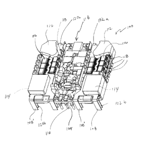
Referring to Figure 1, an electronic module in the form of assembled DC to DC
power
converter 100 is shown according to an embodiment of the invention. Power
converter 100 is
provided to illustrate aspects of the embodiment. It will be appreciated that
other modifications,
adaptations and variations of the embodiments disclosed herein may be made
without departing
from the scope of the invention. Accordingly, the invention is not limited to
electronic modules
in the field of power converters.
As shown, power converter 100 includes four substrates 102 (102a and 102b) and
120
(120a and 120b) mounted to a printed circuit board ("PCB") 104 with two
substrates mounted on
each side of PCB 104. Substrate 120 has a mirror image configuration of
substrate 102. Unless
the particular context suggests otherwise, reference in the following
description to substrate 102
may also include substrate 120. Each substrate 102 carnes electrical
components, which, in the
particular example as shown, are field effect transistors 106 ("FETs").
Substrate 102 is
configured to carry FETs 106, and substrate 102 forms a portion of an
electrical circuit for FETs
106, a power source (not shown), and PCB 104. In this configuration, substrate
102 defines a
single-layer circuit track which connects to a circuit defined in the layout
of PCB 104. As
described in greater detail below, portions of the circuit track in substrate
102 provide windings
for transformer 112 and inductor 114. It will be appreciated that in other
embodiments, electrical
components may include typical analog and digital packaged devices such as
resistors,
capacitors, inductors, transistors, op-amps, LSI components, VLSI components
and hybrids of
analog and digital components. The foregoing list of devices is not
exhaustive. It will be
zioi96as.n _ 6 _
CA 02394403 2002-07-22
t
appreciated that in this art a substrate populated with any electrical
component may be referred
to as a circuit module and that a printed circuit board is also known as,
simply, a circuit board.
In the embodiment, power converter 100 generates a lower voltage, high
current, power
signal from a higher voltage, lower current, input voltage signal. Typical
applications of the
S embodiment take a 24V signal and generate a 1.8V signal at 100 A. Other
conversion
applications can also be implemented. In the power conversion circuit in power
converter 100,
power (at 24V) is provided from a suitable power source. Power is provided to
terminals
(hidden in Figure 1 ), which are similar to terminals 110, but are located at
the back of PCB 104.
Referring to Figs. 1 A and 1 B, the input voltage signal is applied to the
primary windings 112A
of transformer 112. The primary windings are embedded in internal tracks in
internal layers in
PCB 104. The secondary winding 1128 of transformer 112 is formed by a portion
of substrate
102 which is encapsulated by core 112C of transformer 112 within its casing.
The signal carried
from the secondary 1128 winding is regulated by FETs 106 and is then provided
to inductor 114.
Inductor 114 is formed by a part of substrate 102 which is encapsulated by
core 114A contained
casing 1148 of inductor 114. The output of inductor 114 is the final output of
power converter
100, and is provided to leads 108. Leads 108 are mountable into a power bus
(not shown) and
can be soldered into place.
It will be appreciated that transformer 112 and inductor 114 both belong to a
family of
signal transforming components which are known in the art as "magnetics".
Magnetics typically
have a winding such a winding 112A and 114A interacting with a magnetic core,
such as 112C
and 114B respectively. The main feature of a magnetic is the winding. Other
variants on
magnetics include having a winding which is associated with an air core. As
such, for brevity,
any general reference herein to transformer 112 and inductor 114 may use the
term "magnetics",
unless otherwise specifically noted.
When FETs 106 are powered, heat is generated. Heat may also be generated by
PCB 104
and components mounted thereon, as well as, but to a lesser extent, by
transformers 112 and 114.
To remove heat from FETs 106 and PCB components 116, substrate 102 is adapted
to encourage
21019645.11 _ 7
CA 02394403 2002-07-22
the dissipation of the heat. In particular, heat dissipation fins 118 are
provided in substrate 102.
In such a configuration, substrate 102 functions as a heat sink.
Referring to Figures 2A to 8, the manufacturing and assembly process of power
converter
100 is described. First, substrates 102 and PCBs 104 are separately formed
from separate blanks.
Each blank contains a number of identical PCBs (and substrates) carried in a
frame. Each PCB
(and substrate) is populated with a set of its components. Fins 118 are then
bent and formed in
the substrate blanks. The blanks then are mated together and the individual
PCBs and substates
104 are excised from their frames.
Specifically refernng to Figure 2A, a blank, or web, in the nature of a lead
frame 200,
forms an array of substrates 102. Lead frame 200 shares some aspects with
known lead frames.
Known lead frame assemblies are used for manufacturing microelectronic
components such as
semi-conductors or integrated circuit chips. Such lead frame assemblies
generally consist of a
frame having sets of interior leads connected to the frame and a Garner.
Generally, the frame is
flat. An integrated circuit die is typically mounted upon the Garner.
Electrical connections are
made from the leads by fine electrically conductive bonding wires to locations
on the circuit.
Once the inner connections are made, the dies are encapsulated in a protective
resin. The leads
are then excised, and the integrated circuit is separated from the lead frame.
External ends of the
leads form the connection elements to connect the integrated circuit with
other electronic
components, such as electronic components mounted to a PCB.
For manufacturing efficiency, lead frame 200 includes three pairs of
substrates 102. In
the embodiment, lead frame 200 includes three pairs of aligned substrates 102
and substrates
120. This layout is set to align each substrate pair to be aligned with a
corresponding PCB in
PCB frame 400, as shown in Figure 5. Substrates 102 are supported by a
framework 202 which
forms part of the lead frame 200. Framework 202 is mounted to or integrally
formed with
substrates 102, and serves to maintain substrates 102 in a predetermined
orientation for later
mounting to PCB 104. The term "framework" is used herein interchangeably with
the term
"frame". Again, in the embodiment, substrates 120 share similar physical and
dimensional
zioi96as.i1 _ g
CA 02394403 2002-07-22
features of substrates 102, but for the layout of substrates 120 being a
mirror image of substrates
102.
Lead frame 200 is preferably stamped from a single sheet of material such as a
deformable and (electrically and thermally) conductive metal. Stamping is a
relatively
inexpensive manufacturing process. The sheet has a uniform thickness T to
provide uniformity
of substrates 102 which form a part thereof. In other embodiments, uniformity
of the array may
differ. In the embodiment, a bare copper sheet is used for lead frame 200.
Other forming
techniques may be used to form lead frame 200 in other embodiments.
As is well known in the art, the amount and dimensions of copper used in a
substrate
affects the amount of electric current that can be carried by the substrate.
As noted above, when
portions of substrate 102 function as transformer windings, a significant
amount of current may
have to be carried. Accordingly, the cross-section dimensions and length of
the copper sheet
used for lead frame 200 is determined based in part on the amount of current
to be carned. For
example, as one component of the cross-section dimensions, for the substrate
102 as shaped, a
thickness T of about 24 thousandths of an inch ("thou") will allow the
substrate 102 to carry
about 100 amperes, and a thickness T of about 12 thou will allow it to carry
about 50 amperes. It
is desirable to have a sufficient thickness to provide a cross-section which
allows carrying of the
amperage load of the related circuit. Other circuits may have lower amperage
ratings of, for
example, 5, 10, 15, 20 and 25 amps. While placing a relatively thick layer of
copper on the
surface of a PCB is possible, such an arrangement reduces the ability to
provide fine track copper
widths on the PCB surface. As such, SMT components, which generally are used
with fine
copper track widths, may not be efficiently placed on the PCB. Alternatively,
burying the thick
copper layer within the PCB does not allow effective dissipation of heat
carried in the
encapsulated copper layer, and will tend to reduce the number of substrate
layers available for
other design purposes.
Alternatively, depending on the particular function or functions to be
performed by
substrate 102, lead frame 200 may also be made of other material such as a
ceramic, which is not
necessarily electrically or thermally conductive. For example, substrate 102
may be used as a
zioi96as.a _ g _
CA 02394403 2002-07-22
mere Garner for components without substrate 102 forming any direct electrical
connection with
PCB 104.
As noted above, lead frame 200 is stamped from a single sheet of material to
form a
generally planar blank having one or more substrates 102 and a framework 202
connecting and
aligning the substrates 102. Framework 202 includes handling rails 204 or
simply rails 204, for
holding by, or engagement with, assembly machinery (not shown). In the
embodiment, two
generally parallel rails 204A and 204B are formed during the stamping process
with substrates
102 defined therebetween. Rail 204A is connected to each substrate 102 via
tabs 208, and rail
204B is connected to each substrate 102 by tabs which may be later formed into
power leads
108.
Rails 204 may have one or more alignment elements in the nature of registers
or
mounting holes 206 defined therein. Mounting holes 206 permit the assembly
machinery to
engage lead frame 200 to facilitate alignment and mounting of lead frame 200
to a corresponding
PCB frame 400 (see Figure 4). In particular, one method of assembly and
alignment of a PCB
frame 400 to a lead frame 200 may be to use a base (not shown) having posts to
co-operate with
mounting holes in PCB frame 400 and lead frame 200. Accordingly, PCB frame 400
may be
mounted onto the base by aligning the holes in the PCB frame 400 over the
posts, then lead
frame 200 may be mounted and aligned to PCB frame 200 in a similar manner.
Accordingly,
frame 200 may be referred to as an alignment frame.
The basic physical elements of each substrate 102 may be defined by the die of
the stamp
for the blank. As can be seen in Figure 2, fins 118 are defined in the blank.
When substrate 102
is made from a deformable, thermally conductive material, fins 118 can be bent
upward from
lead frame 200 to enhance the heat dissipation abilities of substrate 102.
Excising and forming is
done on lead frame 200 using techniques and tools known in the art. For
example, a fin such as
elongate fin 216 or elongate fin 217 may be formed in substrate 102. For
increased transfer of
thermal energy away from substrate 102, elongate fins 216 and 217 each have a
greater surface
area than fins 118. As shown in Figure 6, elongate fms 216 and 217 also
generally fit within the
general volume otherwise occupied by power converter 100. The number of fins
118, 216 and
21019645.11 - 10 -
CA 02394403 2002-07-22
217 may also be varied to affect thermal transfer from substrate 102. While
fins 118 are shown
as being generally rectangular, other sizes and shapes may be applied
depending on heat transfer
requirements of power converter 100 and on physical space limitations of the
intended
application to which power converter 100 will be applied.
Power leads 108 also serve to dissipate heat from power converter 100. Even if
fins 118,
216 and 217 or power leads 108 are not included with substrate 102, the
substrate 102 itself,
when made of a thermally conductive material, can draw heat away from FETs
106. Further
still, if substrate 102 is not made of a thermally conductive material, it may
still be configured to
perform any one or more of the other functions described herein.
Substrate 102 has a first portion 210A and a second portion 210B, each of
which is
initially physically isolated from the other by a space except for a lead
frame rail section 211
therebetween (this section 211 is removed with rails 204 in a later stage of
manufacture).
Substrate portions 210A and 210B co-operate to define an opening 218, for
receiving a
transformer core (not shown) of transformer 112, and an opening 220, for
receiving a core (not
shown) of inductor 114. Other shaped spaces, gaps and openings may be provided
in other
embodiments by differently shaped first and second portions of substrate 102
for alternative
design, heat transfer or component placement requirements.
As indicated earlier, substrate 102 forms one secondary winding 112B for
transformer
112. The section of substrate 102 which forms winding 112B is indicated at
section 210A(A).
Similarly, the section of substrate 102 which forms winding 114B of inductor
114 is shown at
section 210A(B). Accordingly, substrate 102 is an active part of the power
conversion circuit of
power conversion module 100. It will be appreciated that in other embodiments,
a substrate
similar to substrate 102 may be incorporated into a different electrical
circuit and that the
substrate may have different electrical components attached thereto.
After the lead frame 200 is stamped, it may be placed for processing onto
assembly
machinery such as a conveyor system. Alternatively, lead frame 200 may be
processed
manually. Whether processed manually, using an automated system, or some
combination
2ioi96as.n - 11 -
CA 02394403 2002-07-22
thereof, lead frame 200 is then populated with FETs 106. However, it will be
appreciated that
more manufacturing efficiencies will be possible, generally, with an automated
manufacturing
procedure. Lead frame 200 advantageously permits direct component attachment
using existing
machinery, whether the components are encapsulated or not. When substrate 102
is attached or
mounted to PCB 104, it effectively increases the surface area of PCB 104 so
that the number of
components, such as FETs 106, that can be attached to PCB 104 is increased
while not changing
a footprint of the PCB. When populated in this manner, substrate 102 functions
as an external,
exposed circuit to PCB 104. In the embodiment, FETs 106 are populated onto the
lead frame
200 using known surface mount technology ("SMT") component populating and
soldering
techniques. As described above, lead frame 200 also has alignment elements
enabling the lead
frame 200 to be aligned with a corresponding set of PCBs in a corresponding
PCB frame, to
facilitate manufacturing and assembly of the PCB and its components. When FETs
106 are
soldered onto lead frame 200, FETs 106 are rigidly connected to the lead
frame, allowing FETs
106 to be securely attached to the lead frame, regardless of the spatial
orientation of FETs 106
relative to the lead frame. For example, FETs 106 may be mounted on an
underside of a
substrate.
Refernng to Fig. 3A, FETs 106 are each embodied in a typical SMT S08 package
300.
An exemplary FET 106 comprises a drain terminal 302, a source terminal 304 and
a gate
terminal 306. FET 106 operates as per known FETs. Within S08 package 300,
drain terminal is
connected to pins 308, source terminal 304 is connected to pins 310 and gate
terminal is
connected to pin 312. As described in greater detail below, nib 224 is later
excised from
substrate 102 to electrically isolate the associated pin 312 from its
previously attached substrate
portion 210A or 210B, as the case may be. The remaining pins 308 and 310 on
either side of
SMT package 300 of FET 106 remain connected to substrate portion 210A or 210B
(depending
on the side of FET 106 that the leads 222 are associated with). Accordingly,
pins 308 are
electrically shorted together on either side of substrate portions 210A and
210B and pins 310 are
also electrically shorted together on either side of substrate portions 210A
and 210B. When
FETs 106 are mounted to substrate 102, they are located to having their pins
bridge substrate
portions 210A and 210B. Each pin 308, 310 and 312 makes physical and
electrical contact with
21019645.11 - 12 -
CA 02394403 2002-07-22
a landing and are soldered, bonded or otherwise fixed to landings on substrate
102. Substrate
102 is also formed to include nib 224 for connection to pin 312 of package 300
of FET 106.
FET 106 straddles substrate portions Z 10A and 210B. This configuration
permits a
circuit to be completed between portions 210A and 210B via the contacting pins
of FETs 106
when populated substrate 102 is mounted to a PCB 104. As a result, substrate
102 forms part of
an operable circuit in addition to forming part of the windings of transformer
112. Accordingly,
substrate 102 with mounted FET 106 may be considered to be a circuit module.
Alternatively, if
substrate 102 is not populated with FETs 106, substrate 102 may still form a
portion of a circuit
when combined with PCB 104. It will be appreciated that for a given circuit
configuration and a
given lead layout for a FET 106 (or other component), the arrangement of leads
which are
attached to the portions, and those which are excised, vary depending on the
circuit.
Refernng to Figure 2B, the lead frame 200 of Figure 2A is shown after it has
been
excised and formed. Fins 118 are bent from the plane of lead frame 200 so that
they are oriented
generally perpendicular to the plane of lead frame 200, and are generally
oriented in the same
direction. Fins 118 are preferably oriented away from the side of lead frame
200 which will be
mounted to PCB 104. This configuration encourages the dissipation of thermal
energy away
from substrate 102 and PCB 104 (when PCB 104 is mounted to substrate 102).
Elongate fins
216 and 217 may be similarly bent. The fins, for example fins 118, may be bent
at a second
location to locate at least a portion thereof closer to the components, for
example FETs 106, from
which thermal energy is to be drawn (see also Figure 5).
Referring additionally to Figure 3A, nibs 224 are excised from substrate 102
to isolate
attached FET lead 222 from associated portion 210B. Excising may be done by
using a punch
tool (not shown) to sever nib 224 from substrate 102. Alternatively, substrate
102 may be
trimmed or drilled therethrough in a location adjacent each nib 224. Any other
suitable method
as is known in the art may also be used to excise nib 224 from substrate 102.
While nib 224 is excised from substrate 102 it is still attached on one side
to a FET lead
222. The other side of nib 224 will be aligned and soldered to a land 402 (see
Figure 4) of PCB
21019645.11 - 13 -
CA 02394403 2002-07-22
later in the manufacturing process. When substrate 102 is mounted to PCB 104,
excised nib 104
functions as a riser and serves to span the space between FET lead 222 and
land 402, thereby
electrically connecting FET 106 to PCB 104. This structure may similarly be
used to connect
PCB 104 to other components (not shown) which are mounted to substrate 102, in
order to create
a conductive interface between substrate 102 and PCB 104.
Alternatively, components such as FETs 106 which are mounted to substrate 102,
may
have a particular lead thereof electrically connected to PCB 104 by using an
extended leg (not
shown) that is dimensioned to span the distance between FET 106 and PCB 104.
If this
configuration is employed, then a pathway or void (not shown) defined by
substrate 102 is
located for each extended leg to pass therethrough for connection to PCB 104.
In a further
alternative (not shown), a conductive material, such as solder or a post, may
be added to FET
lead 222 so that it may span thickness T of substrate 102 to electrically
connect to PCB 104. If
solder is used, then sufficient solder material should be provided to ensure
that after reflow there
is enough solder to form an electrical connection between FET 106 and PCB 104.
Refernng to Figure 4, a blank or web in the nature of a PCB frame 400 is used
to form
PCB 104. For manufacturing efficiency, PCB frame 400 includes multiple PCBs
104. In the
embodiment, PCB frame 400 includes three aligned PCBs 104. This configuration
permits each
PCB 104 to be aligned with a corresponding lead frame 400, as shown in Figure
5. PCBs 104
are supported by a framework 404 which forms part of the PCB frame 400.
Framework 404 is
mounted to or integrally formed with PCBs 104, and serves to maintain PCBs 104
in a
predetermined orientation for later mounting to substrate 102.
PCB frame 400 is preferably manufactured as a single part including PCBs 104.
Any
appropriate PCB manufacturing process known in the art may be used. A
preferred
configuration of PCB frame 400 permits mufti-layer PCBs 104 to be manufactured
using such
processes as are known in the art. Once PCB frame 400 is manufactured, it is
populated with
PCB components 116. Preparation of PCB frame 400 may be carried out using
known
manufacturing equipment and methods, including those which employ surface
mount
technology.
21019645.11 - 14 -
CA 02394403 2002-07-22
PCB framework 404 has rails 406 for holding by, or engagement with, assembly
machinery (not shown). Two generally parallel rails 406a and 406b are formed
during the PCB
framework manufacturing process, with PCBs 104 located therebetween. Rail 406a
is connected
to each PCB 104 via tabs 407, and rail 406b is connected to each PCB 104 by
tabs 409.
Spanners 410 connect rails 406a and 406b. Transverse tabs 411 connect spanners
410 to
adjacent PCBs 104. A spanner 410 is located at either end of PCB framework
404. Additional
transverse tabs 411 form interconnections between adjacent PCBs 104 of PCB
framework 404.
Rails 406 have one or more mounting holes 412 defined therein. Mounting holes
412
permit the assembly machinery to engage PCB frame 400 to facilitate alignment
and mounting of
PCB frame 400 to a corresponding lead frame 200.
Each PCB 104 has portions defining openings 414 for receiving a transformer
core (not
shown) of transformer 112, and openings 416 for receiving a transformer core
(not shown) of
transformer 114. Windings (not shown) are sandwiched within each PCB and
encircle openings
414 and 416. Each winding of PCB 104 co-operates with a respective winding of
the magnetics
of transformer 112 and inductor 114, as noted earlier.
Refernng to Figure 5, excised and formed lead frame 200 is mounted by
soldering to
PCB frame 400. Lead frame 200 has portions in the nature of nubs S00 which
align with lands
418 of PCB 104 (see Figure 4; lands 418 are obscured by nubs 500 in Figure 5).
An electrical
connection is made between PCB 104 and substrate 102 at nubs S00 by soldering
substrate 102
to PCB 104. Contact points for nibs 500 for substrate 102 are shown points 122
in Figure 1A. In
the embodiment, points 122 are internally connected via a track in PCB 104.
Lead frame 200
may be attached directly to PCB frame 400 using a PCB reflow process known in
the art.
Alternatively, the lead frame 200 and PCB frame 400 may be attached using a
secondary attach
process using a thermal bar or hand solder process.
It will be appreciated that when substrate 102 is soldered to PCB 104,
substrate 102 may
lie generally flush against PCB 104. Due to manufacturing tolerances, design
requirements and
other reasons, there may be an air gap between the upper surface of PCB 104
and the lower
21019645.11 - 1 S -
CA 02394403 2002-07-22
surface of substrate 102. As assembled, heat produced by PCB 104 is conducted
through
substrate 102 and any components thereon. Accordingly, the surface area of
substrate 102 and
any components thereon is used to dissipate heat from PCB 104. Air flow around
the exposed
surface of substrate 102, either forced, convection or ambient, may assist in
dissipation of heat
from substrate 102.
Frameworks 202 and 404 co-operate to facilitate the alignment of associated
substrates
102 to PCBs 104. Once aligned, substrates 102 and PCBs 104 may be physically
and/or
electrically connected together. If either or both of substrate 102 and PCB
104 are not populated
with components, the lead frame 200 and PCB frame 400 may still be mounted to
one another in
the manner described above. In this way, frameworks 202 and 404 still
facilitate alignment of
the associated substrates 102 and PCBs 104 for mounting.
As noted earlier, whether or not substrate 102 and PCB 104 are populated with
components, lead frame 200 and PCB frame 400 are mounted generally flush to
one another. In
an alternative embodiment, lead frame 200 may have a raised section to form a
spaced region
when mounted on PCB frame 400, as described below and shown in Figures 9A and
9B.
Refernng to Figure 6, the combined lead frame 200 and PCB frame 400 is shown
with
lead frame rails 204 and tabs 208 removed. Lead frame rails 204 and tabs 208
may be removed
at this stage in the assembly of power converter 100 because substrate 102 and
PCB 104 are
attached. Also, at this stage in the assembly process, lead frame leads 108
are formed or bent for
convenient connection to a power supply (not shown). In the embodiment, leads
108 are angled
away from PCB 104 and are generally perpendicular to the plane thereof.
Once frame rails 204 are removed and power leads 108 are formed, PCB 104 is
detached
from PCB framework 404 either by cutting, breaking, or in some other manner
separating it from
PCB framework 404 without damaging power converter 100. For example, PCB
framework 404
may have small holes or perforations 600 defined therein to facilitate
separation of PCB 104
from PCB framework 404. Perforations 600 traverse tabs 407, 409, 411 and 412,
adj acent each
PCB 104, for removal of tabs 407, 409, 411 and 412, and associated rails 406
and spanners 410.
z~o~96as.n - 16 -
CA 02394403 2002-07-22
Referring to Figure 7, as an alternative, before detaching PCB 104 from PCB
framework
404, a second lead frame 700 is mounted to PCB framework 404 on a side thereof
which is
opposite to lead frame 200. The addition of a second lead frame 700 permits
further
implementation of one or more of the features described above for lead frame
200 and its
associated substrates 102. For example, second lead frame 700 may be used to
encourage further
heat dissipation from PCB 104, substrate 102 and associated components
thereof. Second lead
frame 700 may also be populated with components, such as FETs 702, in a
similar manner as
described above for lead frame 200.
Referring additionally to Figure 8, second lead frame 700 is excised and
formed in a
manner similar to that described for lead frame 200. Once excising and forming
is complete,
additional components, such as cores and casings for transformer 112 and
inductor 114, are
mounted to substrate 102 and PCB 104. Power converters 100 are then detached
from PCB
frame 400 as described above for the embodiment having a single lead frame
200. This results in
the isolation of a completed power converter 100, as shown in Figure 1A.
For illustrative purposes, Figure 8 shows an isolated completed, but
unpopulated
substrate 102, in exploded view from PCB 104.
Referring to Figures 9A and 9B, an alternative power converter 900 is shown.
Alternative power converter 900 differs from power converter 100 in that it
has a modified
substrate 901 mounted to a side of PCB 104. Substrate 901 has an offset or
raised section 902
that, when mounted to PCB 104, is spaced from PCB 104. Substrates 904, 906 and
908 are
similarly configured. Because substrates 901, 904, 906, and 908 have similar
configurations,
only substrate 901 will be described. The description herein for substrate 901
generally applies
to substrates 904, 906, and 908 as well.
Raised sections 902 can be post-formed either when lead frame 200 is initially
stamped
or at some stage in the manufacturing process thereafter. Following forming,
which deforms
substrates 102 into substrates 901, substrates 901 are populated, processed
and mounted to PCB
frame 400 in a similar manner as described above for substrates 102.
21019645.11 _ 1 ~~ _
CA 02394403 2002-07-22
Raised section 902 presents two sides for mounting electronic components such
as FETs
106. This enables a greater number of components to be used in roughly the
same footprint as
occupied by power converter 100. Additional components may also be added to
PCB 104.
Raised sections 902 increase the exposed surface area of both substrate 901
and PCB 104. This
increased exposure may facilitate the transfer of heat from PCB 104, substrate
901 and their
associated components. In a manner similar to that used to create fins 118,
216 and 217, fins
910, 912 and 914 may be created. Fins 910, 912 and 914 encourage transfer of
heat away from
power converter 900. Fins 910 and 912 may be bent to opposite sides of
substrate 901 to
facilitate air flow therebetween. In the embodiment illustrated, fins 910 and
912 alternate along
an edge of raised section 902.
As an alternative to raised section 902, substrate 901 may instead be
displaced from PCB
104 using risers (not shown) or some other means to produce a space between
PCB 104 and the
lower surface of substrate 102, to allow placement of components to the
underside of substrate
901, and to enhance heat dissipation for power converter 900.
Referring to Figure 10, alternative power converter 1000 is shown. Power
converter
1000 is similar to power converter 100 except that it has interconnect pins
1001 attached instead
of power leads 108. As described above, while the use of power leads 108 can
increase the
current carrying capabilities of power converter 100, if power requirements
are such that less
current is acceptable, then interconnect pins 1001 may be used instead of
power leads 108.
Refernng to Figure 11, alternative power converter 1100 is shown. Power
converter
1100 is generally similar to power converter 100, but it differs in that the
orientation of power
leads 108 is rotated to form power leads 1101. This configuration of power
leads 1101 permits
attachment to a power supply (not shown) having a different configuration than
the power supply
for power converter 100.
Referring to Figure 12, power converter 900 is shown having an additional
substrate 1200
provided therewith. Additional substrate 1200 is formed from a generally
planar piece of a
thermally conductive material, and has a different configuration than
substrates 102 and 901.
21019645.11 _ 1 g _
~ CA 02394403 2002-07-22
Substrate 1200 is attached directly to or adjacent heat generating components
such as FETs 106,
and functions as a heat sink to encourage transfer of thermal energy away
therefrom. Substrate
1200 may be similarly added to any of the other power converters 100, 900,
1000, and 1100
described above.
Any two or more of the associated components described above could be provided
as a
kit (not shown) for assembling a power converter (such as power converter 100)
or a part
thereof. For example, lead frame 200 may be provided as a system in a kit with
PCB frame 400
for subsequent manufacture into one of the power converters described above.
The kit may also
include any one or more of the associated components such as FETs 106. Other
combinations of
frames, substrates and components may also be provided in a kit for later
assembly. Partially
completed assemblies could also be provided in kit form for later processing
by a purchaser or
assembler.
Those skilled in the art will appreciate that numerous modifications,
adaptations and
variations may be made to the embodiments without departing from the scope of
the invention.
21019645.11 - 19 -