Note: Descriptions are shown in the official language in which they were submitted.
CA 02394458 2002-06-10
WO 01/43181 PCT/IL00/00786
METHODS FOR PRODUCING PACKAGED INTEGRATED CIRCLtIT DEVICES &
PACKAGED I?~'TEGRATED CIRCUIT DEVICES PRODUCED THEREBY
FIELD OF THE INVENTION
The present invention relates to integrated circuits and similar devices
generally
and to methods for the manufacture thereof.
BACKGROUND OF THE INVEI~'TION
An essential step in the manufacture of all integrated circuit devices is
known as
"packaging" and involves mechanical and environmental protection of a silicon
chip
which is at the heart of the inte;rated circuit as well as electrical
interconnection
between predetermined locations on the silicon chip and external electrical
terminals.
At present three principal technologies are employed for packaging
semiconductors: wire bonding, tape automatic bonding (TAB) and flip chip.
~t'ire bonding employs heat and ultrasonic energy to weld gold bonding wires
between bond pads on the chip and contacts on the package.
Tape automatic bonding (TAB) employs a copper foil tape instead of bonding
wire. The copper foil tape is configured for each specific die and package
combination
and includes a pattern of copper traces suited thereto. The individual leads
may be
connected individually or as a group to the various bond pads on the chip.
Flip chips are integrated circuit dies which have solder bumps formed on top
of
the bonding pads, thus allowing the die to be "flipped" circuit side down and
directly
soldered to a substrate. V'ire bonds are not required and considerable savings
in package
spacing may be realized.
The above-described technologies each have certain limitations. Both wire
bonding and TAB bonding are prone to bad bond formation and subject the die to
relatively high temperatures and mechanical pressures. Both wire bond and TAB
technologies are problematic from a package size viewpoint, producing
integrated
circuit devices havin; a die-to-packa<Ie area ratio ranging from about 10% to
60%.
The flip-chip does not prcvide packaging but rather only interconnection. The
interconnection encounters problems of uniformity in the solder bumps as well
as in
WO 01/43181 CA 02394458 2002-06-10 pCT/IL00/00786
thermal expansion mismatching, which limits the use of available substrates to
silicon
or materials which have thermal expansion characteristics similar to those of
silicon.
The patent literature is extremely rich in the area of integrated circuits and
methods for the manufacture thereof.
Described in applicant's published PCT Application WO 95/19645 are methods
and apparatus for producing integrated circuit devices.
The following U.S. Patents and patent applications of the present inventor are
considered to be particularly relevant: 5,716,759; 5,547,906; 5,455,455 and
08/952,019.
SUIvIMARY OF THE INVENTION
The present invention seeks to provide improved packaged crystalline substrate
based devices and methods for producing same.
There is thus provided in accordance with a preferred embodiment of the
present
invention a crystalline substrate based device including a crystalline
substrate having
formed thereon a microstructure and at least one packaging layer which is
sealed over
the microstructure by an adhesive and defines therewith at least one gap
between the
crystalline substrate and the at least one packaging layer.
There is also provided in accordance with a preferred embodiment of the
present
invention a chip scale packaged crystalline substrate including:
a substrate having formed thereon a microstructure; and
at least one chip scale package which is sealed over the microstructure and
defines therewith at least one gap.
There is additionally provided in accordance with a preferred embodiment of
the
present invention a method of producing a crystalline substrate based device
including:
providing a microstructure on a substrate; and
adhesively sealing at least one packaging layer over the microstructure and at
least partially spaced therefrom, thereby to define a gap between the
microstructure and
the at least one packaging layer.
Preferably, at least one packaging layer is sealed onto the crystalline
substrate
using an adhesive, such as epoxy.
In accordance with a preferred embodiment of the present invention, the
crystalline substrate includes silicon, lithium niobate, lithium tantalate or
quartz.
2
WO X1/43181 CA 02394458 2002-06-10 pCT/1L00/00786
Preferably, the at leas: one packaging layer is transparent.
The at least one cavity- may include a single cavity or a plurality of
cavities.
The microstructure may include a micromechanical structure, a microelectronic
structure and/or an optoelectronic structure.
BRIEF DESCRIPTION OF THE DRAWING
Figs. 1A and 1B are pictorial illustrations of a crystalline substrate based
device
having an internal cavity, constructed and operative in accordance with a
preferred
embodiment of the present invention;
Figs. 2A, 2B, 2C & 2D are simplified sectional illustrations of various
crystalline substrate based devices constructed and operative in accordance
with a
preferred embodiment of the present invention, corresponding generally to
Figs. 1A and
1B;
Fig. 3 is a partially cut-away sectional illustration of a crystalline
substrate based
device of the type shown in Figs. 1 A & 1 B;
Figs. 4A, 4B, 4C, 4D & 4E are simplified illustrations of steps in a method
for
producing a packaging layer for use in crystalline substrate based device in
accordance
with a preferred embodiment of the present invention;
Figs. 5A, ~B, ~C, SD, SE, SF, SG, SH & SI are simplified illustrations of
steps in
a method for producing a crystalline substrate based device of the type shown
in Figs.
2A & 2C in accordance with a preferred embodiment of the present invention;
Figs. 6A, 6B, 6C, 6D, 6E, 6F, 6G, 6H, 6I, 6J & 6K are simplified illustrations
of
steps in a method for producing a crystalline substrate based device of the
type shown in
Fig. 2B in accordance with another preferred embodiment of the present
invention;
Figs. 7A, 7B, 7C, 7D, 7E, 7F & 7G are simplified illustrations of steps in a
method for producing a crystalline substrate based device of the type shown in
Fig. 2D
in accordance with another preferred embodiment of the present invention;
Figs. 8A and 8B are illustrations of apparatus typically employed in the
manufacture of a crystalline substrate based devices of the type shown in
Figs. 2A & 2C
in the manner shown in Figs. 5A - SI;
Figs. 9A and 9B are illustrations of apparatus typically employed in the
manufacture of a crystalline substrate based devices of the type shown in Fig.
2B in the
CA 02394458 2002-06-10
WO 01/43181 PCT/IL00/00786
manner shown in Figs. 6A - 6K; and
Figs. 10A and lOB are illustrations of apparatus typically employed in the
manufacture of a crystalline substrate based devices of the type shown in Fig.
2D in the
manner shown in Figs. 7A - 7G.
DETAILED DESCRIPTION OF PREFERRED EMBODIMENTS
Reference is now made to Fi~>s. 1A and 1B, which together illustrate a
preferred
embodiment of integrated circuit device constructed and operative in
accordance with a
preferred embodiment of the present invention. The integrated circuit device
includes a
relatively thin and compact, environmentally protected and mechanically
strengthened
integrated circuit package 10 having a multiplicity of electrical contacts 12
plated along
the edge surfaces 14 thereof.
Preferably, contacts 12 extend over edge surfaces onto the planar surfaces 16
of
the package. This contact arrangement permits both flat surface mounting and
edge
mounting of package 10 onto a circuit board. It is noted that the integrated
circuit
package 10 may include one or more of the following elements (not shown): an
integrally formed dichroic filter, color filter, antireflective coating,
polarizes, optical
grating, integrated wave guide and optical coupling bumps.
In- accordance with a preferred embodiment of the present invention, the
integrated circuit package 10 defines a cavity 18, which is indicated in
phantom lines.
Reference is now made to Figs. 2A - 2D, which illustrate four alternative
preferred embodiments of integrated circuit devices of the general type shown
in Figs.
1A & 1B, constructed and operative in accordance with another preferred
embodiment
of -the present invention. Each of the devices shown in Figs. 2A - 2D includes
a
relatively thin and compact, environmentally protected and mechanically
strengthened
integrated circuit package having a multiplicity of electrical contacts plated
along the
edge surfaces thereof.
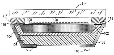
Fig. 2A shows an integrated circuit device including a microlens array 100
formed on a crystalline substrate 102. Underlying the substrate 102 and sealed
thereto
by epoxy 104 is a packaging layer 106, typically formed of glass, along edges
of which
are formed electrical contacts 108, typically defining bumps 110. Conductive
pads 112
preferably connect substrate 102 to electrical contacts 108.
4
WO 01/43181 CA 02394458 2002-06-10 pCT~L00/00786
In accordance with a preferred embodiment of the present invention a packaging
layer 114, typically formed of glass, and associated spacer elements 116, are
sealed, by
means of an adhesive such as epoxy I 18, over substrate 102 so as to define a
cavity 120
between the microlens array 100 and layer 114.
It is appreciated that packa;in~ layer I 14 is preferably transparent and may
have
formed thereon a dichroic filter and/or anti-reflective coating.
Fig. 2B shows an integrated circuit device including an optoelectronic or
electromechanical device 150, such as a chemical sensor, a micromirror array
or an
accelerometer is suspended on a crystalline substrate 152, as by an
electrically
conductive connector 154. Sealed onto substrate 152 is a packaging layer 156
typically
formed of glass, along edges of which are formed electrical contacts 158,
typically
defining bumps 160. Conductive pads 162 preferably connect substrate 152 to
electrical
contacts 158.
In accordance with a preferred embodiment of the present invention a packaging
layer 164, typically formed of Mass, and associated spacer elements 166, are
sealed, by
means of an adhesive, such as epoxy 168, over substrate 152 so as to define
first and
second cavities 170 and 172 between the device 150 and both layer 164 and
layer 156.
It is appreciated that packaging layer 164 is preferably transparent and may
have
formed thereon a dichroic filter and/or anti-reflective coating.
Fig. 2C shows an integrated circuit device including a optoelectronic or
electromechanical device 200 formed on a crystalline substrate 202. Underlying
the
substrate 202 and sealed thereto by epoxy 204 is a packaging layer 206,
typically
formed of glass, along edges of which are formed electrical contacts 208,
typically
defining bumps 210. Conductive pads 212 preferably connect substrate 202 to
electrical
contacts 208.
In accordance with a preferred embodiment of the present invention a packaging
layer 214, typically formed of Glass, and associated spacer elements 216, are
sealed, by
means of an adhesive such as epoxy ~ I 8, over substrate 202 so as to define a
cavity 220
between the device 200 and layer 214.
It is appreciated that packaging layer 214 is preferably transparent and may
have
formed thereon a dichroic filter and/or anti-reflective coating.
Fig. 2D shows a Surface Acoustic Wave (SAW) device including a SAW
WO 01/43181 CA 02394458 2002-06-10 pCT/IL00/00786
propagation surface 250 defined on a crystalline substrate 252, along edges of
which are
formed electrical contacts 258, typically defining bumps 260. Conductive pads
262
preferably connect substrate 252 to electrical contacts 258.
In accordance with a preferred embodiment of the present invention a packaging
layer 264, typically formed of glass, and associated spacer elements 266, are
sealed, by
means of an adhesive such as epoxy 268, over substrate 252 so as to define a
cavity 270
between surface 250 and layer 264.
Reference is now made to Fig. 3, which is a partially cut away illustration of
a
typical integrated circuit device of the type shown in Figs. 1A - 2D, having a
cavity as
indicated by reference numeral 280.
Reference is now made to Fibs. 4A, 4B, 4C, 4D & 4E, which are simplified
illustrations of steps in a method for producing a packaging layer for use in
crystalline
substrate based device in accordance with a preferred embodiment of the
present
invention. As seen in Figs. 4A & 4B, a substrate 300, typically formed of
glass, is
preferably coated with a layer 302 of epoxy based photoresist, typically SU-8
photoresist, commercially available from MicroChem Corp. of Newton, MA, USA.
The photoresist layer 302 is exposed via a mask 304, as shown in Fig. 4C and
washed to define spacers 306 shown in Fig. 4D, which are typically of
rectangular
configuration, as indicated in Fig. 4E. These spacers correspond to spacer
elements 116,
166, 216 and 266 in Fibs. 2A - 2D respectively.
Reference is now made to Fibs. 5A, SB, SC, SD, SE, SF, SG, SH & SI, which are
simplified illustrations of steps in a method for producing a crystalline
substrate based
device of the type shown in Figs. 2A & 2C in accordance with a preferred
embodiment
of the present invention.
As seen in Fib. 5A, a packaging layer 400, typically of the type shown in
Figs.
4D and 4E is provided. Adhesive 402 is applied thereto, preferably adjacent
and
between spacers 406 formed thereon, which correspond to the spacers 306 shown
in
Figs. 4D & 4E respectively and also correspond to spacer elements 116, 166,
216 and
266 in Figs. 2A - 2D respectively. Adhesive 402 is preferably a high
temperature epoxy,
such as EPO-TEK 353ND, commercially available from Epoxy Technology Inc. of
Billerica, MA, USA.
As shown in Fig. 5B, the packaging layer 400, thus prepared, is adhered to a
6
CA 02394458 2002-06-10
WO 01/43181 PCT/IL00/00786
crystalline substrate 404, typically having at least one metal layer thereon
and having
mounted thereon optomechanical or optoelectronic devices of the types
described
hereinabove with reference tc> Figs. 2A & 2C. As seen clearly, a cavity 405 is
defined
between the packaging layer 400 and the substrate 404, in accordance with a
preferred
embodiment of the present invention.
The crystalline substrate 404 is preferably lapped, as shown in Fig. SC and
etched, as shown in Fig. 5D, to define separate substrates 407. Following
etching, the
substrates 407 are adhered via an epoxy layer 408 to an underlying packaging
layer 410,
as shown in Fig. SE.
As seen in Fig. SF, the packaging layer 410 and epoxy layer 408 are
mechanically notched and thereafter electrical contacts 412 and typically
bumps 414 are
formed thereon, as seen in Fig. SG. The resulting assembly is diced as shown
in Fig. 5H
to yield a plurality of packaged integrated circuit devices, as seen in Fig.
5I.
It is appreciated that here and throughout all of the examples described
herein,
the crystalline substrate may be any suitable crystalline substrate and may
comprise, for
example, silicon, lithium niobate, lithium tantalate or quartz.
The manufacturing techniques described hereinabove and hereinbelow may but
need not necessarily include techniques described in any of the following U.S.
Patents
and patent applications of the present inventor/assignee, the disclosure of
which is
hereby incorporated by reference: 5,716,759; 5,547,906; 5,455,455 and
08/952,019.
Reference is now made to Figs. 6A, 6B, 6C, 6D, 6E, 6F, 6G, 6H, 6I, 6J & 6K,
which are simplified illustrations of steps in a method for producing a
crystalline
substrate based device of the type shown in Fig. 2B in accordance with another
preferred embodiment of the present invention.
As seen in Fig. 6A, mounted on a substrate 500, typically formed of Pyrex are
a
plurality of crystalline substrates 502 onto which are formed pads 504 and
onto which
are suspended, as by electrically conductive connectors 506, optoelectronic or
electromechanical devices 508, such as chemical sensors, micromirror arrays or
an
accelerometer, which may correspond to devices 150 of the type shown in Fig.
2B.
As shown in Fig. 6B, a packaging layer 510, typically of the type shown in
Figs.
4D and 4E, is provided having adhesive 512 applied thereto, preferably
adjacent and
between spacers 516 formed thereon, which correspond to the spacers 306 shown
in
7
W~ X1/43181 CA 02394458 2002-06-10 pCT/IL00/00786
Figs. 4D & 4E respectively and also correspond to spacer elements 116, 166,
216 and
266 in Figs. 2A - 2D respectively. Adhesive S 12 is preferably a high
temperature epoxy,
such as EPO-TEK 3S3ND, commercially available from Epoxy Technology Inc. of
Billerica, MA, USA.
As seen in Fig. 6C, the packaging layer S 10, thus prepared, is adhered to
crystalline substrates 502, typically adjacent pads 504. As seen clearly, a
cavity S13 is
defined between the packaging layer S 10 and the substrates 502, and another
cavity 514
is defined between substrates 502, substrate S00 and electromechanical devices
508 in
accordance with a preferred embodiment of the present invention.
The substrate S00 and crystalline substrates 502 are preferably notched, as
shown in Fig. 6D and etched, as shown in Fig. 6E, to define volumes S 15 in
crystalline
substrates S02 which are preferably filled with epoxy S 17, as shown in Fig.
6F.
As seen in Fig. 6G, the substrate 500, the epoxy S 16 and the adhesive S 12
are
then mechanically notched to form a notch SO1, and thereafter electrical
contacts 519
are formed thereon, as by sputtering, as shown in Fig. 6H. Bumps S 18 are
formed
thereon, as seen in Fig. 6I, preferably together with a NiAu coating. The
resulting
assembly is diced as shown in Fig. 61 to yield a plurality of packaged
integrated circuit
devices, as seen in Fig. 6K.
Reference is now made to Figs. 7A, 7B, 7C, 7D, 7E, 7F & 7G, which are
simplified illustrations of steps in a method for producing a crystalline
substrate based
device of the type shown in Fig. 2D in accordance with another preferred
embodiment
of the present invention.
As seen in Fig. 7A, a packaging layer 600, typically of the type shown in
Figs.
4D and 4E is provided. Adhesive 602 is applied thereto, preferably adjacent
and
between spacers 606 formed thereon, which correspond to the spacers 306 shown
in
Figs. 4D & 4E respectively and also correspond to spacer elements 116, 166,
216 and
266 in Figs. 2A - 2D respectively. Adhesive 602 is preferably a high
temperature epoxy,
such as EPO-TEK 3S3ND, commercially available from Epoxy Technology Inc. of
Billerica, MA, USA.
As shown in Fig. 7B, the packaging layer 600, thus prepared, is adhered to a
crystalline substrate 604, typically having at least one metal layer thereon
and having
defined thereon a SAW propagation layer 609 as described hereinabove with
reference
8
CA 02394458 2002-06-10
WO 01/43181 PCT/IL00/00786
to Fig. 2D. As seen clearly, a cavity 607 is defined between the packaging
layer 600 and
the SAW propagation layer 609, in accordance with a preferred embodiment of
the
present invention.
The crystalline substrate 604 can be lapped, as shown in Fig. 7C and notched
partially into the adhesive 602, as shown in Fig. 7D, to define separate
substrates 608.
Following etching, electrical contacts 610 and typically bumps 614 are formed
thereon,
as seen in Fig. 7E. The resulting assembly is diced as shown in Fig. 7F to
yield a
plurality of packaged SAW devices, as seen in Fig. 7G.
Reference is now made to Figs. 8A and 8B, which are illustrations of apparatus
employed in the manufacture of a crystalline substrate based devices of the
type shown
in Figs. 2A & 2C in the manner shown in Figs. 5A - SI. As seen in Figs. 8A and
8B, a
conventional wafer fabrication facility 680 provides complete wafers 681, of
the type
shown in Fig. 5A. Individual wafers 682 are bonded on their active surfaces to
protective layers 683 as shown in Figs. 5A & SB, by bonding apparatus 685,
preferably
having facilities for rotation of the wafer 682, the layer 683 and the epoxy
so as to
obtain even distribution of the epoxy.
The bonded wafer 686 is thinned (Fig. SC) at its non-active surface as by
grinding apparatus 684, such as Model 32BTGW using 12.5A abrasive 687, which
is
commercially available from Speedfam Machines Co. Ltd. of England.
The wafer is then etched (Fig. SD) at its non-active surface, preferably by
photolithography, such as by using conventional spin-coated photoresist, which
is
commercially available from Hoechst, under the brand designation AZ 4562,
using a
mask exposure machine 692 for the exposure of light sensitive photoresist 690
through
the mask 691 and later etching the silicon in a bath 693 using solution 699.
The etched wafer 1000 is bonded (Fig. SE) on the non-active side to protective
layer 686 by bonding apparatus 694, which may be essentially the same as
apparatus
685, to produce a doubly bonded wafer sandwich.
Notching apparatus 695 partially cuts the bonded wafer sandwich of Fig. SE to
the configuration shown in Fig. SF.
The notched wafer 1002 is then preferably subjected to anti-corrosion
treatment
in a bath 696, containing a chromating solution 698, such as described in any
of the
following U.S. Patents: 2,507,956; 2,851,385 and 2,796,370, the disclosure of
which is
9
WO X1/43181 CA 02394458 2002-os-10 pCT/1L00/00786
hereby incorporated by reference.
Conductive layer deposition apparatus 700, which operates by vacuum
deposition techniques, such as a Model 903M sputtering machine manufactured by
Material Research Corporation of the U.S.A., is employed to produce a
conductive layer
on one or more surfaces of each die of the wafer as shown in Fig. SG.
Configuration of contact strips, as shown in Fig. SG, is carried out
preferably by
using conventional electro-deposited photoresist 701, which is commercially
available
from DuPont under the brand name Primecoat or from Shipley, under the brand
name
Eagle. The photoresist 701 is applied to the wafers 707 in a photoresist bath
assembly
702, which is commercially available from DuPont or Shipley.
The photoresist 703 is preferably light configured by a UV exposure system
704,
which may be identical to system 692, using a mask 705 to define suitable
etching
patterns. The photoresist is then developed in a development bath 706, and
then the
wafer is etched in a metal etch solution 708 located in an etching bath 710,
thus
providing a conductor configuration such as that shown in Fig. SG.
The exposed conductive strips shown in Fig. SG are then plated, preferably by
electroless plating apparatus 712, which is commercially available from Okuno
of
Japan.
The wafer is then diced (Fig. 5H) into individual pre-packaged integrated
circuit
devices. Preferably the dicing blade 714 should be a diamond resinoid blade of
thickness 4 - 12 mils. The resulting dies appear as illustrated generally in
Fig. 5I.
Reference is now made to Figs. 9A and 9B, which are illustrations apparatus
employed in the manufacture of a crystalline substrate based devices of the
type shown
in. Fig. 2B in the manner shown in Fibs. 6A - 6K. As seen in Figs. 9A and 9B,
a wafer
fabrication facility 780 provides complete wafers 781, of the type shown in
Fig. 6A
mounted onto a substrate, such as a Pyrex substrate 782. Individual wafers 781
are
bonded on their active surfaces to protective layers 783 as shown in Figs. 6B
& 6C, by
bonding apparatus 784, preferably having facilities for rotation of the wafer
781, the
layer 783 and the epoxy so as to obtain even distribution of the epoxy.
Notching apparatus 794 partially cuts the bonded wafer sandwich 793 of Fig. 6C
to the configuration shown in Fig. 6D. The notched wafer 796 is then etched in
a silicon
etching solution 798 in a bath 1010. The etched voids 1012 in wafer 1014 are
filled with
CA 02394458 2002-06-10
WO 01/43181 PCT/IL00/00786
epoxy 1016, using a dispenser 0018 to fill the voids 1012, to obtain epoxy
filled voids
1020. The wafer 1022 is notch ~d again using apparatus 1024 through the epoxy
filled
trenches 1020.
The notched wafer 1028 is then preferably subjected to anti-corrosion
treatment
in a bath 1030, containing a chromating solution 1032, such as described in
any of the
following U.S. Patents: 2,507,956; 2,851,385 and 2,796,370, the disclosure of
which is
hereby incorporated by reference.
Conductive layer deposition apparatus 800, which operates by vacuum
deposition techniques, such as a Model 903M sputtering machine manufactured by
Material Research Corporation ofthe U.S.A., is employed to produce a
conductive layer
on one or more surfaces of each die of the wafer as shown in Fig. 6G.
Configuration of contact strips, as shown in Fig. 6E, is carried out
preferably by
using conventional electro-deposited photoresist 801, which is commercially
available
from DuPont under the brand name Primecoat or from Shipley, under the brand
name
Eagle. The photoresist is applied to the wafers 803 in a photoresist bath
assembly 802,
which is commercially available from DuPont or Shipley.
The photoresist 807 is preferably light configured by a UV exposure system 804
using a mask 805 to define suitable etching patterns. The photoresist is then
developed
in a development bath 806, and then etched in a metal etch solution 808
located in an
etching bath 810, thus providing a conductor configuration such as that shown
in Fig.
1B.
The exposed conductive strips shown in Fig. 6G are then plated, preferably by
electroless plating apparatus 812, which is commercially available from Okuno
of
Japan.
The wafer is then diced (Fig. 6H) into individual pre-packaged integrated
circuit
devices. Preferably the dicing blade 814 should be a diamond resinoid blade of
thickness 4 - 12 mils. The resulting dies appear as illustrated generally in
Fig. 6K.
Reference is now made to Fills. 10A and 10B, which are illustrations apparatus
employed in the manufacture of a crystal line substrate based device of the
type shown
in Fig. 2D in the manner shown in Fibs. 7A - 7G. As seen in Figs. 10A and 10B,
a
conventional wafer fabrication facility 880 provides complete wafers 881, of
the type
shown in Fig. 7A. Individual wafers 881 are bonded on their active surfaces to
WO X1/43181 CA 02394458 2002-06-10 pCT/IL00/00786
protective layers 883 as shown in Figs. 7A & 7B, by bonding apparatus 882,
preferably
having facilities for rotation of the wafer 881, the layer 883 and the epoxy
so as to
obtain even distribution of the epoxy.
Notching apparatus 894 partially cuts the wafer 883 of Fig. 7E to the
configuration shown in Fig. 7F.
The notched wafer 884 is then preferably subjected to anti-corrosion treatment
in a bath 896, containing a chromating solution 898, such as described in any
of the
following U.S. Patents: 2,507,956; 2,81,385 and 2,796,370, the disclosure of
which is
hereby incorporated by reference.
Conductive layer deposition apparatus 900, which operates by vacuum
deposition techniques, such as a Mode( 903M sputtering machine manufactured by
Material Research Corporation of the U.S.A., is employed to produce a
conductive layer
on one or more surfaces of each die of the wafer as shown in Fig. 7G.
Configuration of contact strips, as shown in Fig. 7E, is carried out
preferably by
using conventional electro-deposited photoresist 901, which is commercially
available
from DuPont under the brand name Primecoat or from Shipley, under the brand
name
Eagle. The photoresist 901 is applied to the wafers 903 in a photoresist bath
assembly
902, which is commercially available from DuPont or Shipley.
The photoresist 920 is preferably light configured by a UV exposure system 904
using a mask 905 to define suitable etching patterns. The photoresist is then
developed
in a development bath 906, and then etched in a metal etch solution 908
located in an
etching bath 910, thus providing a conductor configuration such as that shown
in Fig.
1B.
The exposed conductive strips shown in Fig. 7G are then plated, preferably by
electroless plating apparatus 912, which is commercially available from Okuno
of
Japan.
The wafer 913 is then diced (Fig. 5H) into individual pre-packaged integrated
circuit devices. Preferably the dicing blade 914 should be a diamond resinoid
blade of
thickness 4 - 12 mils. The resulting dies appear as illustrated generally in
Fig. 7G.
It will be appreciated by persons skilled in the art that the present
invention is
not limited by what has been particularly shown and described hereinabove.
Rather the
scope of the present invention includes both combinations and subcombinations
of
12
CA 02394458 2002-06-10
WO 01/43181 PCT/IL00/00786
various features described hereinabove as well as modifications and variations
thereof
which would occur to a person of skill in the art upon reading the foregoing
description
and referring to the drawings and which are not in the prior art.
13