Note: Descriptions are shown in the official language in which they were submitted.
CA 02394761 2008-01-07
1
STEP WAVE POWER CONVERTER
BACKGROUND OF THE INVENTION
This invention relates generally to step wave power converters for
transforming
power from power sources supplying DC voltage input into AC power. More
specifically,
illustrative embodiments of the invention relate to step wave power converters
for providing
greater input control over multiple DC power buses and for more accurately
simulating
single- or multiple-phase AC waveforms. While illustrative embodiments of the
invention
are particularly directed to the transformation of power from DC power sources
to AC power,
it should be noted that AC power sources can be readily converted to DC power
sources
through the use of a rectifier. Therefore, the scope of this invention is not
limited to strictly
DC-to-AC power conversion.
Prior art patents and publications describe various single-phase step wave
power
converters for transforming DC voltage input into a step wave AC output. FIG.
1 is a
schematic illustration showing one example of a prior art power converter.
Referring to FIG.
1, one single-phase step wave power converter of the prior art uses one
transformer 2 for each
step of the step wave output. A single DC power source is used to supply power
to each of
the transformers 2 in the power converter. Each transformer 2 has three
windings, including
two primary windings P1, P2 and one secondary winding S. The two primary
windings P1
and P2 are electrically coupled to the DC power source through four gates Gl-
G4. The gates
G1-G4 control the flow of current through the primary windings Pl, P2 in order
to produce a
step of the AC output from the secondary winding S. The two primary windings
P1, P2 in
each transformer 2 are identical to each other except that they are oppositely
connected to the
DC voltage source. Because of their reverse connections, they induce opposite
polarity
voltage in the secondary winding S. The secondary windings S of the
transformers are
connected together in series so that their outputs can be combined to produce
the step wave
AC output.
In operation, the gates G1-G4 are controlled to alternately pulse DC current
through
the primary windings P1, P2. Current flow through a positive polarity primary
winding P1
induces a positive step output from the corresponding secondary winding S,
while,
conversely, the flow of current through a negative polarity primary winding P2
induces a
CA 02394761 2002-06-18
WO 01/47095 PCTIUSOO/26788
2
negative step. Steps from the secondary windings S of all of the transformers
2 are added
together to form the overall AC waveform. Consequently, pulsing DC current
through the
primary windings P 1, P2 at the appropriate time intervals causes the
secondary windings S to
output an approximate AC waveform.
U.S. Patent No. 5,373,433 issued to Thomas (Thomas) provides an improvement in
the art with respect to single-phase power inverters operating from a single
DC power source.
Specifically, Thomas discloses switching bridges for controlling DC voltage
input into
multiple transformers from a single source. Each switching bridge includes
four switches
arranged in two parallel lines, each of which has two series connected
switches. The
switching bridges are controlled so that the transformers produce either a
positive, zero, or
negative output voltage step at a given time. According to Thomas, the
transformers
"preferably have turns ratios that are multiples of each other in order to
provide both good
resolution and a wide dynamic range of the [AC output] signal." Col. 5,11. 58-
62. For
example, Thomas explicitly discloses a single-phase power converter having
three
transformers capable of producing voltage outputs from their secondary
windings of 15V,
45V, and 13 5V, respectively. The output voltages from the secondary
windings of all of
the transformers are combined in series. Thomas produces a fairly accurate AC
waveform by
controlling timing and sequencing of the voltage contributions from the three
transformers to
transition sequentially through each of twenty-seven different possible
overall output voltage
levels. A special decoder circuit is also provided to prevent accidental
shorting across the DC
voltage input which would occur if two switches in a series connected pair
were closed at the
same time. Despite its improvements, Thomas does not contemplate either the
use of
multiple power sources or three-phase operation.
Another prior art topology is described in U.S. Patent No. 5,631,820 issued to
Donnelly et al. (Donnelly). Donnelly provides an improvement in the art by
using three gates
instead of four to control current flow through primary transformer windings.
Also, although
using transformers having two primary windings and one secondary winding,
Donnelly's
switching architecture allows each primary winding to be used to produce
either a positive or
a negative step, rather than only one or the other. Donnelly also provides an
improvement in
the art by contemplating the use of multiple power sources, but fails to
provide seamless
integration and management of the multiple power sources based on their
performance
characteristics. Donnelly also discloses a three-phase power converter
topology that has nine
CA 02394761 2002-06-18
WO 01/47095 PCT/US00/26788
3
gates and one three winding, three-phase transformer per step.
Other prior art patents and publications also describe three-phase step wave
power
converters for converting DC voltage from one or more DC power sources to a
step wave AC
output. Referring to FIG. 2, one example of a prior art three-phase step wave
power converter
includes multiple three-phase transformers 4, each having three windings (two
primary P1, P2
and one secondary S) per phase per step. The configuration of each phase is
similar to the
single-phase arrangement of the prior art described above with reference to
FIG. 1. Each
phase of each transformer includes two primary windings Pl, P2 and a secondary
winding S.
The two primary windings Pl, P2 of each phase are identical to each other
except for their
opposite connections to the DC power source. Four switches Gl-G4 are used to
control
current flow through the primary windings P1, P2 of each phase. The switches
are used to
alternately pulse DC voltage through the primary windings P1, P2 in order to
generate steps
of the AC waveform for that particular phase from a corresponding secondary
winding S.
The contributions output from the secondary windings S of the transformers for
a given phase
are combined together in series to produce the step wave AC output for that
phase.
Unfortunately, this prior art configuration is bulky, requiring a three
winding, three-
phase transformer 4 controlled by 12 gates for each step. Also, each primary
winding Pl, P2
contributes only one positive or one negative step towards the overall AC
waveform output
and the total number of steps of the AC output directly corresponds to the
number of primary
windings used to produce the output. To get better resolution in this three-
phase AC
waveform output, therefore, more transformers must be added to the system,
further
increasing its bulkiness.
It should be noted that in each of the prior art three-phase step wave
converters, the
three-phase transformers 4 used are wye-wye transformers, meaning that both
the primary P1,
P2 and secondary windings S are arranged in wye configurations. This
configuration is
presumably used to avoid voltage contention which occurs between delta and wye
connections in delta-wye transformers.
A further drawback of each of the prior art power converters is that the step
wave AC
output is generally blocky as a result of the mere addition of positive and/or
negative block
steps to form the AC waveform output. Although blocky AC waveforms are
acceptable for
many applications, they are less than desirable for use in many modern
electronic devices
such as computers, televisions, etc., which perform better and last longer
when power is
CA 02394761 2008-01-07
4
supplied to them using a closely regulated AC power supply.
Therefore, the industry faces several problems related to conventional step
wave power
conversion. First of all, the industry has been unable to seamlessly integrate
power from
multiple power sources based on their performance characteristics. The
industry has also failed
to produce a step wave AC output that more closely approximates an ideal AC
wavefonn.
Additionally, the industry has been unable to produce a three-phase step wave
AC power output
in a more efficient manner. The industry has further failed to enhance the
resolution of the AC
waveform output from a three-phase step wave power converter without
increasing the number
of primary transformer windings. Furthennore, the industry has not succeeded
in allowing a
single power source to selectively supply power to multiple transformers when
other power
sources become disabled or go offline. Nor has the industry succeeded in
preventing backfeed
to the power grid or in allowing any DC power source connected to the
converter to be charged
from any of the other power sources connected thereto.
Accordingly, the industry would be benefitted by a step wave power conversion
method
and apparatus which provides seamless integration between multiple power
sources. The
industry would be further benefitted by a step wave AC output which more
closely
approximates an ideal AC waveform. The industry is in further need of a more
efficient step
wave power converter. The industry would also be benefitted by a method of
converting DC
voltage into three-phase power output with enhanced resolution with simpler
circuitry. The
industry is in still further need of a step wave power converter which allows
a single power
source to selectively supply power to multiple transformers when other power
sources become
disabled. Still further needs in the industiy include preventing backfeed to
the power grid and
allowing any DC power source with storage capability connected to the
converter to be charged
from any of the other power sources connected to the converter.
SUMMARY OF THE INVENTION
Illustrative embodiments of the invention may seamlessly integrate power from
multiple power sources based on their performance characteristics.
Illustrative embodiments may also produce a step wave AC output that more
closely
approximates an ideal AC waveform.
CA 02394761 2008-01-07
Illustrative embodiments may also produce three-phase AC power output in a
more
efficient manner.
Illustrative embodiments may also enhance the resolution of the step wave
power
output from a three-phase step wave power converter without increasing the
number of
5 transformer components.
Illustrative embodiments may also selectively allow a single power source to
supply
power to multiple transformers when one or more other power sources become
disabled.
Illustrative embodiments may also prevent backfeed from the DC power buses to
the
input power grid and allow any of the DC power sources connected to the
converter to be
charged from any of the other power sources connected to the converter.
Illustrative embodiments may provide a significant improvement in the art by
enabling an improved step wave power converter for converting DC voltage input
into a step
wave AC output. The step wave power converter may be provided with multiple
transformers configured to receive DC voltage from a plurality of power
sources. Each of the
transformers may include a primary winding and a secondary winding. The
transformers
may each be configured to supply a step for a step wave AC output. Bridge
circuits may be
supplied for controlling input of DC voltage into the primary windings of the
transformers.
Steps for the step wave AC output may be output from the transformer secondary
windings
based upon the input provided to the primary windings. Source management
circuitry may
manage which power source(s) supplies DC voltage to each of the bridge
circuits. The
management circuitry may provide seamless power switching between the
plurality of power
sources based on each power source's performance characteristics. The step
wave AC output
can be a single-or multi-phase AC output. A pulse-width modulator can also be
provided to
the step wave power converter to modulate the input into a selected primary
winding. In this
way, the step wave AC output can be fine-tuned in substantial conformance with
an ideal AC
waveform.
A three-phase step wave power converter according to one embodiment of this
invention includes multiple three-phase transformers. Each three-phase
transformer has
primary and secondary windings. The three-phase transformers are configured to
receive DC
voltage from one or more power sources into their primary windings and to
supply one or
more steps for each phase of a three-phase step wave AC output from their
secondary
windings. A plurality of bridge configurations or circuits are also supplied,
each of which is
CA 02394761 2002-06-18
WO 01/47095 PCT/US00/26788
6
made up of multiple gate pairs arranged in parallel. Each gate pair includes
two or more gates
arranged in series. Opposite ends of each of the primary windings of each
transformer are
connected between gates in separate gate pairs of a corresponding bridge. Each
bridge circuit
is thereby configured to control current flow across the primary windings of
its corresponding
transformer. Preferably, the transformers are arranged having a delta-wye
configuration in
which primary windings are coupled in a delta arrangement and secondary
windings are
arranged in a wye configuration. When configured in this way, the resolution
of the three-
phase step wave AC output can be enhanced by managing characteristics of the
voltage
transformation between the delta primary winding configurations and the wye
secondary
winding configurations.
A method for enhancing a three-phase step wave AC output from a three-phase
step
wave power converter is also provided. The three-phase step wave power
converter has
multiple three-phase transformers having primary and secondary windings, with
each
transformer arranged in a delta-wye configuration. The method begins by
receiving one or
more DC voltage inputs into the step wave power converter. Steps of the three-
phase step
wave AC output are generated from the secondary windings by controlling timing
and
sequencing of the DC voltage inputs into the primary windings. Voltage phase
characteristics
of the delta-wye transformation are managed to increase the number of steps in
the three-
phase step wave AC output.
Yet another embodiment of the invention provides a step wave power converter
similar to those previously described, but which also includes cross-tie
circuitry to allow one
of the power sources to supply power to two or more transformers when one or
more of the
other power sources becomes unstable, inoperative, or goes offline. This cross-
tie circuitry
includes gated connections between two or more of the DC buses. Each power
source can
further be provided with cut-off gates to allow it to be readily disconnected
from the input
system(s).
A still further embodiment of a step wave power converter includes an
isolation
switch for isolating at least one of the power sources from the input power
grid to prevent or
gate backfeed to the grid. It should also be noted that isolation switches can
be provided for
each of the power sources, to isolate each of them from each of the other
power sources as
well as from the input power grid. When each of the power sources are isolated
from each
other, bi-directional circuitry can further be provided for allowing any of
the DC power
CA 02394761 2008-01-07
7
sources to be charged from any other of the power sources. Providing isolated
power sources
also allows DC power to be supplied by a rectified variable frequency and
voltage input.
In a further embodiment, a method for enhancing the characteristics of a step
wave
AC output from a step wave power converter is provided in which a DC voltage
is supplied
to the step wave power converter. The DC voltage is transformed into a
plurality of steps of
the step wave AC output. Significantly, the DC input voltage is pulse-width
modulated such
that the step wave AC output more closely approximates an AC waveform. This
method
works particularly well when DC input voltages are provided to multiple
transformers and
when the input voltage to a selected one or more of the transformers is pulse-
width
modulated while holding the inputs to one or more of the other transformers in
a constant on
or off state. This allows fine-tuning of the step wave AC output in
substantial conformity
with an ideal AC waveform.
In accordance with another illustrative embodiment, there is provided a step
wave
power converter. The step wave power converter includes a plurality of
transformers each
configured to receive a DC voltage from one of multiple independently
generated power
sources. Each transformer includes a primary winding and a secondary winding
and is
configured to selectively supply one or more steps for a step wave AC output.
The step wave
power converter further includes a plurality of bridge circuits each for
controlling a different
one of multiple different DC voltage inputs from one of the multiple
independently generated
power sources into the primary windings in order to output steps for the step
wave AC output
from the secondary windings. The step wave power converter further includes
source
management circuitry for individually managing how each of the DC voltage
inputs are
switched by the bridge circuits, according to each power source's performance
characteristics.
In accordance with another illustrative embodiment, there is provided a method
for
enhancing a three-phase step wave AC output from a three-phase step wave power
converter
having a plurality of three-phase transformers arranged with delta-wye primary
to secondary
winding configurations. The method includes receiving one or more DC voltage
inputs into
the step wave power converter, generating one or more steps of the three-phase
step wave AC
output from the secondary windings of the three-phase transformers, and
increasing the
number of steps in the three-phase step wave AC output by controlling timing
and sequencing
of the DC voltage inputs into the primary windings of the delta-wye three-
phase transformers
CA 02394761 2008-01-07
7A
to take advantage of inherent properties of the delta-wye transformation.
In accordance with another illustrative embodiment, there is provided a step
wave
power converter. The step wave power converter includes a plurality of
transformers
configured to receive DC voltage inputs from one or more DC power sources or
rectified AC
power sources. Each transformer includes a primary winding and a secondary
winding and is
configured to supply a step of a step wave AC output. The step wave power
converter further
includes a plurality of bridge circuits for controlling the DC voltage inputs
into the primary
windings of the transformers in order to output steps for the step wave AC
output from the
secondary windings of the transformers. The step wave power converter further
includes
control circuitry for controlling the amount, duration, and polarity of DC
voltage supplied to
each of the primary windings of each of the transformers.
It will be readily apparent to those of skill in the art that the above
described features
and advantages can be combined in numerous ways not limited to those
combinations
explicitly described herein. Furthermore, the foregoing and other aspects,
features, and
advantages of the invention will become more readily apparent from the
following detailed
description of preferred embodiments of the invention which proceed with
reference to the
accompanying drawings.
BRIEF DESCRIPTION OF THE DRAWINGS
FIG. 1 is a schematic illustration of a conventional single-phase step wave
power
converter for converting DC voltage from a single power source into a step
wave AC output.
FIG. 2 is a schematic illustration of a conventional three-phase step wave
power
converter for converting DC voltage from a single power source into a three-
phase step wave
AC output.
FIG. 3 is a schematic diagram of a single-phase step wave power converter
configured
to receive and manage DC voltage inputs from multiple power sources according
to one
embodiment of the present invention.
FIG. 4 is a series of graphs illustrating the generation of a single-phase
step wave AC
output from a step wave power converter, such as the one illustrated in FIG.
3, having four
transformers.
FIG. 5A is a schematic illustration of a step wave power converter, similar to
the one
CA 02394761 2002-06-18
WO 01/47095 PCT/US00/26788
8
illustrated in FIG. 3, further including cross-tie circuitry and cut-off gates
for selectively
providing or disabling input from one of the DC power sources to one or more
transformers
according to another embodiment of the present invention.
FIG. 5B is a schematic illustration of a step wave power converter, similar to
the one
illustrated in FIG. 3, for controlling power inputs from multiple sources
according to yet another
embodiment of the invention.
FIG. 6 is a schematic illustration of a three-phase step wave power converter
according
to yet another embodiment of the present invention, showing an improved bridge
arrangement
and delta-wye transformer configurations.
FIG. 7A is a more detailed schematic illustration of the three-phase step wave
power
converter according to FIG. 6, further showing insulated gate bipolar
transistor (IGBT) modules
containing bridge circuitry, driver boards for driving the bridge circuitry,
control boards for
controlling the driver boards, and series connections between secondary
windings of the
transformers for each phase, among other things.
FIG. 7B is an enlarged view of the transformer configuration of the converter
in FIG.
7A.
FIG. 7C is a block diagram of a control board having both software and
hardware
components for controlling the step wave power converter of FIG. 7A according
to a preferred
embodiment of the present invention.
FIG. 8 is a voltage versus time graph showing a step wave AC output from a
delta-wye
three-phase step wave power converter similar to FIG. 8A but having enhanced
resolution
resulting from careful control of voltage characteristics in the delta-wye
transformers.
FIG. 9 is a flow chart illustrating a method for more accurately approximating
an ideal
AC waveform using a hybrid of step wave power conversion and pulse-width
modulation
according another embodiment of the invention.
FIG. 10 is a voltage ratio versus time graph illustrating operation of the
hybrid step wave
and pulse-width modulation power conversion method of FIG. 9.
FIG. 11A is a schematic illustration of a prior art uninterruptible power
supply system
for providing backup power.
FIG. 11 B is a schematic illustration of the step wave power converter of the
present
invention for use as a backup power system according to yet another embodiment
of the
invention.
CA 02394761 2002-06-18
WO 01/47095 PCT/US00/26788
9
DETAILED DESCRIPTION
The step wave power converter (SWPC) of this invention is an innovative power
converter designed around a unique platform that allows it to have a wide
range of uses
beyond those of conventional power converters. These uses extend beyond the
usual task of
converting power from a single DC source to AC power. One such use includes
consolidation, integration and supervisory control of multiple power sources
through a single
SWPC while isolating each source so that each can operate at optimum
efficiency. The
power sources connected to the SWPC can include diesel or gas generators, wind
turbines,
solar photovoltaic (PV) cell arrays, hydro-electric generators, batteries, gas
turbine generators,
fuel cells, etc. Yet another use is in backup power supply systems, including
integration,
isolation, and management of the power sources that comprise the backup power
supply
system. Still another use is managing the power for power generators installed
in the
distributed generation mode. Another use is end of grid and in line voltage
and power quality
regulation. Further uses include standard 60 Hz or customized frequency
regulation; the
ability to feed reactive power to a grid or an off-grid load on demand; and
the provision of a
programmable microprocessor controller that is customized and optimized, as
required, for
each application.
Specific embodiments of the present invention will now be described in more
detail.
FIG. 3 is a schematic illustration of a single-phase step wave power converter
for receiving
and managing DC voltage inputs from multiple power sources according to one
embodiment
of the present invention. According to this embodiment, DC buses 5 receive
power from the
power sources and supply it as a DC voltage input to one or more bridge
circuits 10. Each
bridge circuit 10 preferably consists of an insulated gate bipolar transistor
(IGBT) module
having four IGBT switching gates G1-G4, which are controlled by a driver board
in response
to signals from a control board. Each IGBT switching gate G1-G4 is preferably
fitted with an
antiparallel diode D1-D4, respectively, to allow shorting current to flow.
Although IGBT
switching gates are preferred, the gates can include HEXfets or other
semiconductor power
switching devices and a corresponding antiparallel diode. In this embodiment,
a single two
winding (one primary P and one secondary S) transformer 15 is used for each
step.
Single-phase shorting using the four gate bridge 10 involves closing the two
gates G1,
G2 on the positive inputs (the positive transistors) or the two gates G3, G4
on the negative
CA 02394761 2002-06-18
WO 01/47095 PCT/US00/26788
5
inputs (the negative transistors). Closing the gates in this manner allows
shorting current to
flow through one diode and one gate of a shorted transformer 15, thereby
imposing a null
potential across the primary winding P of the shorted transformer. Shorting is
important for
allowing power supplies to be dynamically added or removed from a transformer
without
10 affecting the transformer's winding ratio requirements.
FIG. 4 illustrates the production of a single-phase step wave AC output from a
step
wave power converter, such as the one described above with reference to FIG.
3. Referring
now to FIG. 4, a step wave AC output is produced as follows. In a step wave
power converter
having four transformers, each transformer produces an output from its
secondary winding
according to a voltage input into its primary winding and the transformer
winding ratio. Each
of these outputs forms a building block, or step, of an overall AC output. The
outputs from
all of the secondary transformer windings are added together in series to
simulate the AC sine
wave.
Generally, the process for producing the step wave output proceeds by turning
on each
of the transformers sequentially at a specified time and then leaving them on
for a given
period of time before sequentially deactivating them. Specifically, this
process begins by
turning on a first transformer at a zero reference time tO. The activation of
the first
transformer activates step one of the step wave output. Step one remains
activated while
other steps are added. At a first point in time tl, a second transformer is
turned on and its
voltage output is combined with the output of the first transformer, thereby
activating step
two. Similarly, at a second point in time t2, a third transformer is turned on
and its voltage
output is added to that of the others to activate step three of the step wave
output. Likewise
also, at a third point in time t3, a fourth transformer is turned on to
activate step four.
At a later specified time, the step wave production process is reversed to
step the AC
waveform back down. This is accomplished by sequentially turning the
transformers off at
fourth, fifth, sixth, and seventh points in time t4, t5, t6, and t7. Turning a
transformer off
preferably includes shorting a voltage across the primary winding of the
transformer as
described above. Although this reverse process can proceed by turning off the
transformers in
any order, a preferred method proceeds by deactivating the transformers in the
order they
were activated. Accordingly, the first transformer is deactivated first, the
second transformer
next, and so on. Specifically, step one is deactivated by turning off the
first transformer at the
fourth point in time t4. Step two is deactivated at the fifth point in time t5
by turning off the
CA 02394761 2002-06-18
WO 01/47095 PCT/US00/26788
11
second transformer. Similarly, step three is deactivated at the sixth point in
time t6 by turning
off the third transformer. And, finally, step four is deactivated at the
seventh point in time t7
by turning off the fourth transformer. By deactivating the transformers in the
order they were
activated, balancing of the transformer duty cycles is achieved.
Although not shown, after all of the transformers have been turned off, the
waveform
building process is repeated in order to build the later 180 degrees (or
negative half) of the
AC sine wave. The process for producing the negative half of the waveform is
the same as
for the positive half just described, except with negative voltage polarity.
Referring again to FIG. 3, a positive step for the AC waveform is generated by
closing
the first positive switch G1 and the second negative switch G4 in one of the
bridge circuits.
A negative step for the AC waveform is generated by closing the first negative
switch G3 and
the second positive switch G2 in one of the bridge circuits. A shunt of the
transformer
primary P is generated by closing either both positive switches G1, G2 or both
negative
switches G3, G4.
In summary, the steps of the simulated AC waveform of FIG. 4 are produced by
sequentially enabling and disabling DC voltage input into the primary windings
of multiple
transformers at specified points of time. In some embodiments, each step may
be formed
from the voltage contributions of only one transformer. In other embodiments,
however, each
step may be formed from the voltage contributions of more than one
transformer.
Voltage control of the step wave AC output is established by varying the
number of
transformers active at any given time as well as the duty cycle associated
with each of those
transformers. The transformers can also be sized to assure that any number
less than the total
number of transformers are capable of producing rated output voltage.
Additionally, by
adding steps and by varying the duty cycle of any given step, a wide range of
output voltages
can be derived. Additionally, step width can be varied to generate the proper
waveform and
RMS voltage.
When multiple power sources are provided to a step wave power converter, it is
sometimes desirable to maintain the ability to cross connect any of the power
sources to any
number of transformers in the converter. Consequently, according to a
preferred embodiment
of this invention, each power source connected to the SWPC is supplied with a
bypass switch.
Bypass switches allow the SWPC to switch off an abnormal power source. Bypass
switches
further allow the SWPC to prevent backfeed to the grid. Bypass switches can be
added to any
CA 02394761 2002-06-18
WO 01/47095 PCT/US00/26788
12
SWPC configuration by supplying cut-off gates to the power source input lines
as illustrated
in FIG. 5A. This allows the gating mechanism of the grid source to be blocked
when needed.
Another layer of protection can be achieved using the cross-tie approach
described below.
FIG. 5A shows additional DC source management circuitry including a cross-tie
arrangement for interconnecting multiple power sources with multiple
transformers. In the
cross-tie arrangement, a step wave power converter is provided with gated
interconnections,
called cross-ties, between DC buses 5. The gates on the interconnections are
referred to as
cross-tie gates. The cut-off gates described above are included on each power
source's
positive and negative input lines to isolate that power source from the other
power sources
and the grid. In normal operation, the power source cut-off gates are closed
to allow power to
be supplied from each of the power sources while the cross-tie gates are open
to provide
isolation between DC buses. When one of the power sources fails or is
disconnected,
however, a degrading DC bus 5 is sensed. The cut-off gates associated with the
failed source
then open to isolate and prevent further contribution of power from the
compromised power
source, and the cross-tie gates close to allow a still functioning power
source to supply power
to the DC bus 5 for the compromised power source. This control mode assures
seamless
transfer between power sources while still maintaining isolation between them.
Although
FIG. 5A shows only two power sources, it should be appreciated that this
embodiment is
scalable to include any number of power sources and cross-tie devices.
Therefore, more than
two sources can be added in this scheme.
An improvement in the art realized by yet another embodiment of this invention
results from the provision of bi-directional circuitry between the isolated
power sources. Bi-
directional circuitry between isolated power sources gives the SWPC of this
invention the
ability to charge any of the DC sources connected to the SWPC from any of the
other sources
connected to the SWPC. In other words, this circuitry enables a bi-directional
capability on
any of the DC buses 5 but maintains their isolation from one another. For
example, in a
SPWC where a battery and a photovoltaic (PV) cell array comprise two of the
power sources,
the battery can be charged from the PV array while still maintaining the
array's isolation from
the battery. This is a significant innovation because the batteries can stay
at a relatively
constant voltage while the PV maximum power point voltage fluctuates.
A still further advantage provided by the use of isolated DC buses is the
ability of the
SWPC of this invention to allow variable speed operation of any combination of
rotating or
CA 02394761 2002-06-18
WO 01/47095 PCT/US00/26788
13
fixed power generation means. For example, a variable speed diesel, a variable
speed
windmill, and a PV array can all be run through a single SWPC when isolation
is maintained
between each of the DC buses. In other words, when the diesel's rectified DC
bus is isolated
from the rectified DC bus of the windmill and the PV array, each of the
sources can operate at
any desired speed or voltage level without interfering with the other sources.
FIG. 5B illustrates still other embodiments of this invention which are also
configured
to provide multiple power source management through power source management
circuitry.
One such embodiment includes multiple high frequency input converters tied to
each DC bus
5, while yet another includes a combined multiple input converter. By using
more than one
high frequency input converter tied to each DC bus 5, or a combined multiple
input converter,
each input may contribute as much of the power to the overall system as
desired. The top
circuit illustrated in FIG. 5B shows multiple high frequency input converters
tied to each DC
bus 5. In this embodiment, power inputs from each of the multiple power
sources are run
through a separate isolation circuit which can also contain pulse width
modulation circuitry.
One of the input power sources, i.e., Input #1, can be an input power grid.
The outputs from
all of the isolation circuits are combined together and supplied to the DC bus
5. Each DC bus
5 can then be used to supply power to a transformer. The transformer would
receive DC
voltage input from the DC bus, which receives power from one or more power
sources,
including the input power grid, through the isolation circuit. The isolation
circuit can thereby
isolate the DC bus from the input power grid to prevent backfeed to the grid
from the DC bus.
The circuit illustrated at the bottom of FIG. 5B illustrates a combined
multiple input
converter tied to a DC bus 5. In this converter, multiple high frequency
DC/DC, PFC, and
AC/DC converter inputs from multiple sources may be converted to a common DC
bus 5. By
providing proper feedback control, each input can supply a regulated portion
of the power
used in the inverter. The portion of the power supplied by each input can be
adjusted by the
control board. This feature can also be incorporated into a single, high
frequency converter
circuit, with multiple inputs, that synchronizes control and reduces
components.
Multiple power source management is particularly beneficial where some or all
of the
power sources produce non-uniform power outputs, such as photovoltaic cells,
windmills, etc.
According to this invention, such sources could be used to provide a large
amount of the
power when their strength is high, but be used to supply less of the power as
they weaken.
The control signal for each input converter will determine the amount of power
transferred
CA 02394761 2002-06-18
WO 01/47095 PCT/US00/26788
14
from each power source. This embodiment thereby facilitates "soft" transfers
between input
sources. Unlike "hard" power transfers, where a power source is either
connected to or
disconnected from the system, "soft" power transfers allow each power source
to contribute a
desired percentage of the power to each of the transformers. Also, this
invention allows
power sources to be slowly ramped-in or ramped-out when being connected to or
disconnected from the system, helping to prevent voltage spikes and provide a
more uniform
power supply. These types of multiple power source control can be utilized
with either
single-phase or three-phase power converters.
Still another embodiment of this invention provides improvements in the art
specifically with respect to three-phase step wave power converters. This
embodiment is the
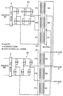
unique SWPC configuration shown in FIG. 6. FIG. 6 is a schematic illustration
of a three-
phase step wave power converter including an improved bridge architecture 20
and delta-wye
transformers 25. Specifically, this embodiment utilizes a unique step wave
power converter
topology consisting of multiple three-phase transformers 25, each arranged
with primary
windings PA, PB, PC in a delta configuration and secondary windings SA, SB, SC
in a wye
configuration. Voltage flow across the primary windings PA, PB, PC of each
transformer is
controlled by six gates Gl-G6 configured in a bridge circuit 20. One or more
power sources
can be used to supply power to the bridge circuits 20 through their respective
DC buses 5.
Each of the gates G 1 -G6 in a bridge circuit 20 includes an insulated gate
bipolar transistor
(IGBT) fitted with an antiparallel diode to allow shorting current to flow. A
primary benefit
of this new topology is that it requires only six gates GI-G6 and one three-
phase transformer
25 per step (having only one primary and one secondary winding per phase)
rather than the
nine or twelve gates and the more complex transformer configurations of the
prior art.
As mentioned above, the connections between the primary windings of each of
the
three-phase transformers 25 in this embodiment are arranged in a delta
configuration. Each
three-phase transformer 25 includes a single primary winding PA, PB, or PC and
a single
secondary winding SA, SB, or SC for each phase. In the delta configuration, a
first end of a
phase A primary winding PA and a second end of a phase C primary winding PC of
one
transformer 25 are coupled together and connected to that transformer's bridge
circuit 20
between two gates G1 and G4 in a first series connected gate pair. Similarly,
a second end of
the phase A primary winding PA and a first end of the phase B primary winding
PB are
coupled together and connected to the bridge circuit 20 between two gates G2
and G5 in a
CA 02394761 2002-06-18
WO 01/47095 PCT[USOO/26788
5
second series connected gate pair. Finally, a first end of the C phase primary
winding PC and
a second end of a B phase primary winding PB are coupled together and
connected to the
bridge circuit 20 between two gates G3 and G6 in a third series connected gate
pair. The
secondary windings SA, SB, SC of each three-phase transformer 25 are arranged
in a wye
10 configuration, with all of the secondary windings SA, SB, or SC of the same
phase being
connected together in series.
Operation of the three-phase transformers 25 using the six gate bridge 20 will
now be
described in more detail. Voltage across the primary windings PA, PB, PC of
the
transformers is controlled to induce the steps of the AC waveform output for
each phase A, B,
15 C through the corresponding secondary windings SA, SB, SC. Each of the
transformers 25
directly contributes one step to the AC output of each phase. Specifically,
when a voltage is
applied across a transformer's primary winding corresponding to one of the
phases, the
corresponding secondary winding produces a step for that phase of the AC
output.
Furthermore, similar to the single-phase embodiment, a voltage is shorted
across one or more
of the primary windings of the three-phase transformer 25 in order to shunt
them. Three-
phase shorting (i.e., shorting of all three phases) using a six gate bridge 20
involves closing
the three positive transistors G1-G3 or the three negative transistors G4-G6.
Closing either
set of three gates allows shorting current to flow through a combination of
diodes and gates
so that a null potential is imposed across all three primary windings PA, PB,
PC of the
shorted transformer.
Furthermore, each of the primary windings PA, PB, PC of the transformer 25 may
have a potential or be shunted at different times based upon the operation of
the six gates G 1-
G6. For instance, the phase A primary winding PA will be on when either of two
sets of
gates G1, G5 or G2, G4 are closed. Positive polarity voltage is applied across
the phase A
primary winding PA when a first positive gate G1 and a second negative gate G5
are closed.
Conversely, reverse polarity voltage is applied to the phase A primary winding
PA when a
second positive gate G2 and a first negative gate G4 are closed. Phase A is
shorted and
turned off, however, when either the two positive gates G1, G2 or the two
negative gates G4,
G5 connected to opposite ends of the phase A primary winding PA are closed.
Similarly, the
phase B primary winding PB will be on when either of two sets of gates G2, G6
or G3, G5 are
on. Positive polarity voltage is applied across the phase B primary winding PB
when the
second positive gate G2 and a third negative gate G6 are closed. Reverse
polarity voltage is
CA 02394761 2002-06-18
WO 01/47095 PCT/US00/26788
16
applied across the phase B primary winding PB when a third positive gate G3
and the second
negative gate G5 are closed. The phase B winding PB is turned off when either
the two
positive gates G2, G3 or the two negative gates G5, G6 connected to its
opposite ends are
closed. Phase C is again similar. Positive polarity voltage is applied across
the phase C
primary winding PC when the third positive gate G3 and the first negative gate
G4 are both
closed. Reverse polarity voltage is applied across the phase C primary winding
PC when the
first positive gate G1 and the third negative gate G6 are closed. Finally, the
phase C primary
winding PC is turned off when either the two positive gates Gl, G3 or the two
negative gates
G4, G6 connected to its ends are closed.
It should be appreciated that the gates G 1-G6 may be controlled in any number
of
combinations in order to produce the desired steps for each phase.
Accordingly, by
controlling the six gates Gl-G6 of the bridge circuit 20, voltage of either
positive or negative
polarity or a null potential can be applied across the primary windings for
each phase. In this
way, the desired contribution to the overall AC waveform can be output from
the phase's
corresponding secondary winding based on control of the bridge circuit 20.
FIG. 7A is a detailed schematic illustration of a three-phase step wave power
converter (SWPC), such as the one described above with reference to FIG. 6.
FIG. 7B is an
enlarged view of the transformer arrangement of the SWPC of FIG. 7A. Referring
to FIG.
7A, IGBT modules provide the bridging circuitry 20 for control of DC power
into the primary
transformer windings of three-phase transformers. Power is supplied from a
power source to
DC buses 5. The DC buses 5 supply DC voltage input to terminals N and P of
each IGBT
module 20, where terminal N is the DC negative terminal and terminal P is the
DC positive
terminal. Each of the IGBT modules 20 produces three separate outputs A, B,
and C from its
three output terminals U, V, and W. These outputs are the building blocks for
the A, B, and
C phases of the three-phase AC output.
In this embodiment, four IGBT modules 20 are used to control when DC voltage
inputs are supplied to the primary transformer windings of four three-phase
transformers 25
to produce the steps (or building blocks) for each of the three phases. Of
course, more or
fewer than four IGBT modules 20 and transformers 25 could be used. The ratio
between
IGBT modules 20 and transformers 25 is typically one to one. Each three-phase
transformer
25 includes three primary windings and three secondary windings (one of each
for each
phase). Also, in this embodiment, each IGBT module 20 is supplied power from a
single,
CA 02394761 2002-06-18
WO 01/47095 PCT/US00/26788
17
separate DC power bus 5, each of which is connected to its own power source
(Power
Sources 1-4). It should be appreciated, however, that any number of power
sources may be
connected to any one or more of the DC buses 5, as has been described above
with respect to
other embodiments of the invention.
The IGBT modules 20 regulate the flow of current from their DC bus 5 across
the
primary windings of their corresponding transformers 25 in order to produce
the steps of the
three-phase AC waveform. The four IGBT modules 20 are each controlled by one
of four
driver boards 22 that are, in turn, controlled by a control board 24. More
specifically, a
control algorithm, resident on the control board 24, controls signals sent to
each of the four
driver boards 22 that, in turn, send signals to activate the gates inside of
each of the four
IGBT modules 20 at the appropriate times. The control algorithm thereby
controls the
activation of the IGBTs in a desired sequence to produce the step wave AC
output.
Referring now to FIG. 7B, outputs A, B, and C from the IGBT modules 20 are fed
to
the primary windings PA, PB, PC of their corresponding three-phase
transformers T 1-T4 to
control voltage therein. Each transformer T 1-T4 directly produces a single
step for each
phase from its secondary windings SA, SB, SC based on current flowing through
its
corresponding primary windings PA, PB, PC. The four transformers Tl-T4 are
configured
having secondary windings of the same phase connected together in series. The
three phases
are also connected into a wye configuration on each of the secondaries.
As mentioned above, the three-phase step wave power converter of this
embodiment
has control circuitry including three types of control devices, as shown in
FIG. 7A. The
control board 24 has all programmed information and is the heart of the
control system. The
driver boards 22 are an interface between the control board 24 and the IGBT
modules 20.
The IGBT modules 20 are the power electronics that allow the electrical side
of the step wave
power converter to operate. The IGBT modules 20 are preferably commercially
available
Powerex six pack modules made by Powerex Intellimod and are unmodified from
their
original condition. The driver boards 22 are generally known to those skilled
in the art. The
control board 24 is being designed and built specifically for use with the
single- and three-
phase step wave power converters of this invention, a schematic representation
of which is
shown in FIG. 7C. Resident on the control board 24 is the micro-controller
chip that is used
to control all aspects of the step wave power converter. The software in the
control board 24
enables the unique switching aspects of the invention.
CA 02394761 2002-06-18
WO 01/47095 PCT/US00/26788
18
The control board software manages the operation of the entire SWPC. It
controls the
operation of all of the IGBT switches within each of the IGBT modules 20 that
in turn
characterize the AC waveform. The proper timing for operating each of the
switches in each
IGBT module 20 is crucial to generating acceptable AC power quality. The
software also
provides features such as the ability to maintain loading for individual input
sources; control
of AC output voltage and current; phasing and grid synchronization; the
ability to monitor
and isolate gates and or gate driver logic failures; the ability to skew step
wave timing to
reduce harmonic distortion; step wave/pulse-width modulation (PWM) hybrid
control; the
ability to combine multiple inputs with different voltages and ratings; the
ability to provide
feedback to power sources to allow following of output loading; and the
ability to allow
heavy loading of single inputs, such as batteries, for a short period of time
during transient
conditions to allow for sources with a slower reaction time to pick up loads.
Although the
foregoing and other features are preferably implemented by software, it should
be noted that
some or all of these aspects of the invention may be performed in analog
circuitry rather than
by software.
In a basic three-phase step wave power converter, each phase of the AC
waveform can
be constructed in the same way as was described previously with respect to the
single-phase
step wave AC output shown in FIG. 4. Although the basic stepping procedure
works very
well with the single-phase power converter, however, using it directly on the
three-phase
power converter of this invention produces contention because of the delta-wye
configurations of the gates and transformers. This contention is very
detrimental to the AC
power output quality. Remarkably, however, in the three-phase delta-wye
configuration, the
timing of the IGBT switches can actually be controlled in such a way (i.e., to
adjust phase
shift instead of step width) that the transformer phase shift is used in a
constructive, rather
than a destructive, manner. A phase management controller, such as the control
board 24,
may be used to control the switches to use transformer phase shift
constructively.
Therefore, although the arrangements of the primary and secondary windings of
three-
phase transformers can be configured many different ways, it becomes
advantageous in this
invention to configure the primary windings in a delta arrangement and the
secondary
windings in a wye arrangement. Specifically, this delta-wye arrangement, when
properly
controlled, allows the resulting step wave to be made to contain n+2 steps,
where n is the
number of transformers involved in producing the AC waveform. The AC waveform
thus
CA 02394761 2002-06-18
WO 01/47095 PCT/US00/26788
19
produced includes additional steps caused by the addition of three phase-
shifted primary
waveforms.
FIG. 8 is a voltage versus time graph showing an enhanced step wave AC output
produced by carefully controlling the IGBT switches to use phase shift between
delta and wye
transformer winding configurations constructively. As shown, constructive use
of
transformer contention can provide a six step waveform using only four
transformers, rather
than the conventional four step waveform.
To obtain the improved results described above, the invention provides a
unique
method for controlling the IGBT switches that allows the three-phase step wave
power
converter to produce an AC output voltage with higher resolution. This higher
resolution
includes an increased number of output voltage steps while using the same
number of IGBT
switches and transformers. This unique control method combines the normal
phase shift
combinations in the delta-wye transformer configuration with smart transformer
phase shift
control logic to reduce harmonics. In other words, by intelligently activating
and deactivating
the switches on the IGBT boards according to the natural delta-wye phase
response, the step
wave power converter of this embodiment provides an enhanced step wave AC
output signal.
As discussed previously, use of conventional step wave switching algorithms to
produce a simulated AC output is well-known. It is also quite common for
conventional
inverters to utilize a pulse width modulation (PWM) switching algorithm to
approximate a
sine wave. PWM refers to the change of the on and off times (duty cycle) of
pulses, such that
the average voltage is the peak voltage times the duty factor. In such PWM
inverters, a sine
wave is approximated using a series of variable-width pulses. None of the
prior art power
converters, however, have combined a step wave output with PWM. A significant
improvement in the art is provided by this invention through a novel
combination of step
wave power conversion and PWM.
Fortunately, both step wave and PWM processes can cycle power sources in any
sequence as well as control individual input source loading. Several
advantages therefore
result from the combination of these two approaches. These advantages include,
among other
things, closer approximation to a sine wave than with either of the prior art
approaches alone,
fewer losses than in conventional pulse-width modulation approaches,
elimination of the need
for rapid switching of full line voltage, and greater adaptability of the AC
waveform output.
Accordingly, still another preferred embodiment of this invention utilizes a
unique
CA 02394761 2002-06-18
WO 01/47095 PCTIUSOO/26788
5
combination of step wave and PWM algorithms to generate a hybrid step wave/PWM
AC
output that very closely approximates an ideal AC sine wave (i.e., potentially
less than 2%
total harmonic distortion). FIG. 9 is a flow diagram of a preferred algorithm
for combining
PWM with step wave power conversion. This flow chart illustrates a process for
creating a
10 hybrid step wave/PWM waveform that closely approximates an ideal AC
waveform. It
should be noted that this algorithm can be incorporated as firmware on a micro-
controller
with supporting analog circuitry or it can be completely analog or completely
micro-controller
based.
Generally, according to this novel approach, PWM is used to improve the
transition
15 edges of each step of a step wave AC output. The hybrid step wave/PWM
system uses a
pulse-width modulator to modulate the power input into a selected one of the
transformers
while inputs into the other transformers are held in a steady on or off
position, to maintain the
basic steps of the AC step waveform. PWM waves are thereby used in the step
wave
transitions to refine the envelope of the simulated AC waveform. These smaller
PWM pulses
20 can be filtered to help produce a well regulated sine wave that has very
little harmonic
distortion. In this way, the step wave process is used to approximate an AC
sine wave on a
large scale while the PWM process provides higher refinement to the sine wave
approximation. The combination of using PWM for one or more transformers while
using
step wave power conversion technology for others is unique.
FIG. 10 is a graph that further illustrates the hybrid process for creating an
AC
waveform as described above using the algorithm of FIG. 9. The vertical axis
of the graph
represents the ratio of the total voltage output V(out) from series combined
secondary
transformer windings of the SWPC to a peak voltage Vsetpoint of an ideal sine
wave. The
horizontal axis is a time axis. The bottom graph represents the PWM output
supplied to a
selected primary winding of one of the transformers. Generally, as illustrated
by the graph of
FIG. 10, the hybrid step wave/PWM approach works by adding the step waves
together to
generate a rough estimate of a sine wave while pulse-width modulating voltage
input signals
during transitions to smooth the edges of the steps.
Referring to FIGs. 9 and 10, the hybrid step wave/PWM algorithm will now be
described in detail. First, however, the parameters of the algorithm need to
be defined. V(i)
is used to represent the voltage applied at a primary winding i, where i = 1,
2, 3, 4, . . . , k; and
where k represents the total number of transformer primary windings used in
generating the
CA 02394761 2002-06-18
WO 01/47095 PCTIUSOO/26788
21
AC waveform. As noted previously, V(out) represents the combined output
voltage from the
series connected secondary transformer windings and Vsetpoint indicates the
maximum
voltage level of an ideal AC waveform. The PWM envelope represents the limits
within
which the PWM operation takes place, such that the unfiltered pulses are bound
by the PWM
envelope.
When the hybrid step wave/PWM process begins, the combined output voltage
V(out)
is at zero and the parameter i is set to 1. PWM of a DC input voltage V(1)
into a first primary
winding of a first transformer therefore begins. Accordingly, the input
voltage V(1) begins to
be gradually supplied to the first primary winding, such that the first
transformer is turned on.
As the voltage V(1) supplied to the first primary winding is modulated and
filtered, it
gradually increases, as shown by the PWM output graph 26 at the bottom of FIG.
10. The
output voltage from the first transformer's secondary winding and the combined
output
voltage V(out) increase correspondingly. This input voltage V(1) is
continuously modulated
as shown by signal 28 until the PWM level reaches 100% for that step at time
30. Once
PWM for that step reaches 100%, the input voltage V(1) into the first primary
winding is
continuously turned on, as represented by line 32, and the parameter i is then
incremented by
one so that an input voltage V(2) into a second primary winding of a second
transformer can
then be modulated, as represented by signa134.
The PWM process described above is repeated for the voltage inputs to each of
the
primary windings until the last required primary winding k is reached. When
this occurs (i.e.,
when i becomes equal to k), pulse width modulation of the input voltage V(k)
into the final
primary winding begins and continues until the overall output voltage V(out)
becomes equal
to the maximum voltage Vsetpoint of the ideal AC waveform. When the output
voltage
V(out) reaches this point, it is at its maximum desired value and must
therefore begin to be
decreased. To decrease the output voltage V(out), i is reset to 1 and the PWM
process is
reversed.
It should be noted that during modulation of each of the voltage steps, the
combined
output voltage level V(out) is continuously tested to see if it has reached
its maximum desired
value Vsetpoint. As long as the output voltage V(out) remains below the
maximum,
however, PWM of the current step continues until it reaches 100% for that
step, as described
above. When the voltage output level V(out) reaches its maximum desired value,
i is reset to
1 and the PWM process is reversed so that the voltage can be gradually
reduced, whether or
CA 02394761 2002-06-18
WO 01/47095 PCTIUSOO/26788
22
not all of the primary windings have been used.
The PWM process continues by gradually reducing PWM of input voltage V(1) to
zero, as represented by signal 36. Once PWM reaches 0% for that step, its
input voltage V(1)
is turned off continuously and i is incremented by one so that the input
voltage V(2) into the
second primary winding can be modulated, as represented by signal 38. This
process
continues for the voltage inputs for each of the primary windings 1- k as they
are each
gradually reduced to zero. After PWM of the final input voltage V(k) (signal
40) has been
completed and the voltage output V(out) is zero (at time 44), the parameter i
is again reset to
1. The entire process then repeats, except this time with negative polarity as
shown in 42.
As a result of the hybrid step wave/PWM process described above, it is
believed
possible to create a simulated AC waveform with less than 2% total harmonic
distortion.
This invention therefore provides a significant improvement in the art by
enabling a SWPC
which produces a simulated AC waveform which very closely approximates an
ideal AC
waveform.
A few specific applications for this invention will now be described further.
One
specific application for the use of an SWPC having multiple, controllable,
isolated source
inputting is in hybrid renewable power systems. SWPCs of this invention can
seamlessly and
efficiently integrate renewable energy sources such as hydro, wind, and solar
power with
conventional generators such as diesel and gas turbines in off-grid, end-of-
grid, and on-grid
applications without compromising the efficient operation of the conventional
or the
renewable power generator units. Using such an SWPC permits the renewable
power sources
to be used as the primary sources while still ensuring continuous operation,
thereby reducing
fuel consumption of the conventional power generators.
Yet another use for the present invention is in backup power systems. Backup
power
systems are used to provide power to facilities when the utility grid fails.
These systems
usually consist of a diesel generator (the primary power supply when operating
off-line),
batteries that provide temporary power during generator start-up, a power
inverter that inverts
the DC battery or generator output to AC power, and a static switch that
transfers the load
from the utility grid to the backup power supply when needed. This entire
system is
conventionally referred to as an uninterruptible power supply (UPS).
Unfortunately, most
UPS systems suffer from one significant shortcoming-if one of the major
components fails,
the entire system is compromised.
CA 02394761 2002-06-18
WO 01/47095 PCT/US00/26788
23
More specifically, in a typical UPS system, such as the one shown in FIG. 11A,
a
utility grid 50 and a backup power system (generator) 52 are not synchronized.
A transfer
switch 56 selects between the two power source input lines #1 and #2 depending
on which
power source 50 or 52 is desired. When the utility grid 50 fails, the backup
power line #2 is
activated to supply power from the backup power source 52. One or more
batteries 54
provide temporary DC power that is inverted to AC power for the user. After
the generator
52 comes to normal operating speed, power will be provided solely by the
generator 52. A
rectifier 57 is used to rectify the power from the utility grid 50 or the
generator 52 to DC
power. An inverter 58 inverts the incoming DC power to AC power. Because of
this
interdependent component configuration, if any one of the components fails,
the entire system
is compromised.
Unlike the conventional system, the SWPC of this invention, when used in a UPS
application as schematically illustrated in FIG. 11 B, can accommodate and
integrate multiple
power sources 50, 52, 54. The ability to integrate multiple power sources
gives the SWPC 18
important advantages over the typical UPS systems. First of all, the invention
eliminates the
need for the transfer switch 56 (see FIG. 11A) that is used with many UPS
systems. This
invention therefore provides truly seamless "uninterruptible" power. This
invention also
preferably isolates each power source 50, 52, 54 from the system to provide
continuous
voltage regulation. If one of the power sources, such as the utility grid 50,
becomes inactive
or is deliberately disconnected, this embodiment of the invention will
regulate the power
output using the remaining power sources 52, 54. This feature can eliminate
costly down
times by allowing scheduled service of power supplies without affecting the
user. When
combined with the rugged and reliable design of the SWPC 18 relative to
commercial
inverters that reside within the UPS, this architecture is much more reliable
and useful than a
typical UPS system.
The SWPC 18 can also condition the power from the utility grid that is to be
used
with sensitive electronics-a process that conventionally requires additional
equipment
provided by the end user. This provides improved efficiency, regulation, and
isolation over
the use of ferro-resonant transformers, as are conventionally used. The
flexibility of the
SWPC 18 also gives the end user room for expansion or modernization of power
sources.
For example, an existing diesel generator 52 or battery bank 54 could be
replaced with fuel
cells as they become available.
CA 02394761 2002-06-18
WO 01/47095 PCT/US00/26788
24
Yet a further application of this invention is in integrating power from
photovoltaic
(PV) cell or battery arrays. PV cells and batteries are power sources for
which the SWPC of
this invention is ideally suited. This is because these DC sources are
typically made up of
multiple, independent "strings". PV arrays, for example, typically consist of
multiple strings
of PV cells. Larger battery banks are also typically arranged as parallel
strings of batteries
and will benefit from use of the SWPC. Each string delivers power as a DC
output voltage.
The SWPC 18 can treat each string as an independent source and electrically
integrate the
multiple strings, while maintaining isolation between them. This is a key
advantage of the
SWPC 18 because if one or more strings malfunction, the SWPC 18 can continue
to deliver
utility- or electronic-grade AC power from the still-functioning strings.
Additionally, the SWPC 18 of this invention can cater to various nominal DC
voltage
levels among the strings. Existing inverter systems deal with nominal DC
voltage levels
through individual voltage regulators on each string or by merging all of the
DC power on a
single DC bus and then inverting the power from the bus to AC power. In some
cases,
inverters are attached to each string and the AC power from each inverter is
combined to feed
the load. The SWPC 18 drastically simplifies and improves the power conversion
architecture compared with prior art inverters for PV arrays allowing maximum
power point
tracking of each input.
A still further application of this invention exists with respect to fuel
cells. Fuel cells
create electricity using an electrochemical process. They differ from
batteries, which also use
an electrochemical process, in that they consume hydrogen and must therefore
have fuel
continuously provided. The type of fuel used to generate hydrogen varies and
depends on the
reforming process for which each system is designed. Fuel cells are well
suited for
distributed generation, but each system must be tailored to the application
that it will serve.
Some applications may require higher power quality than others; some may need
to be
interconnected with the utility grid; some may require several fuel cells to
be paralleled
together; while some may implement co-generation where waste heat of the fuel
cell is used
along with the electrical energy. All these applications require power
conditioning and
custom electrical interconnections with the end user's facility.
The electricity generated from fuel cells is also DC and must be regulated or
converted to AC for user consumption. Conventionally, this is accomplished by
using a
power converter that is often not integrated into the design. The SWPC 18 of
this invention
CA 02394761 2002-06-18
WO 01/47095 PCTIUSOO/26788
5
offers clear advantages over present techniques. One primary advantage in fuel
cell
integration offered by the SWPC 18 is parallel operation of multiple fuel
cells where each
unit may be individually loaded. Another advantage is the ability to follow
fuel cell voltage
versus loading curves and limits.
10 Two conventional methods exist for consolidating the power of multiple fuel
cells
servicing a single user. One method is to use voltage regulators for each fuel
cell and to have
a common bus to which these voltage regulators feed power. The power from the
common
bus is then converted by a single power converter and fed to the user. A
second method is to
use a power converter for each fuel cell, combine the converted power and feed
it to the user.
15 Both of these techniques are costly because of the duplication of system
components for each
fuel cell.
Referring again to FIGs. I 1A and 11B, the SWPC 18 has a distinct advantage
over the
prior art described above. Specifically, one or more power sources, i.e., 52,
54, for the SWPC
18 can be a fuel cell. By replacing the battery banks 54 with fuel cells, the
SWPC 18 allows
20 each fuel cell 54 to operate at peak efficiency by isolating each fuel cell
54 from the others, as
with the other power sources already described above. The SWPC 18 converts the
power to
AC and supplies it to the user. This simplifies the architecture and allows
one or more of the
fuel cells 54 to be taken off-line without any adverse effects.
Still further benefits of this invention exist with respect to grid-connected
applications
25 that have one or more inputs from the grid. In present input grid-connected
applications, the
fuel ce1154 is connected to an inverter in synchronization with the utility
grid 50. It is
disconnected from the grid 50 (i.e., for servicing) using a transfer switch
56. The SWPC 18
of this invention offers a clear advantage over the transfer switch 56. Both
the utility grid 50
and the fuel ce1154, or multiple fuel cells 54, are used as power sources for
the SWPC 18.
The SWPC 18 conditions the power for the user and isolates each fuel cel154
from the utility
grid. The SWPC 18 allows each fuel cell 54 to operate under the preferred
conditions for fuel
efficiency or co-generation. In addition, since all power sources are isolated
by the SWPC 18,
there is no need for a costly transfer switch 56 in the event one of the
sources fails. The
SWPC 18 will simply use the remaining power sources 50, 52, 54 to create high
quality
power.
Fuel cells 54 can also provide power when the grid 50 is not active or when
there is no
grid available. When power from the utility grid 50 is lost, the fuel cel154
will provide
CA 02394761 2002-06-18
WO 01/47095 PCT/US00/26788
26
backup emergency power for the user. For UPS systems, the fuel ce1154 can
effectively
replace the diesel generator source 52, which is commonplace today.
The invention's ability to integrate multiple power sources further gives the
end user
the ability to expand the system power capacity in the future without costly
system upgrades
or the purchase of an entirely new system. With simple software modifications,
the SWPC 18
of this invention can be upgraded to accommodate multiple fuel cells,
interconnection with
the utility grid, or to parallel other types of power sources with the fuel
cell.
Having described and illustrated the principles of the invention in several
preferred
embodiments thereof, it should be apparent that the invention can be modified
in arrangement
and detail without departing from such principles. Particularly, the features
and advantages of
all of the various embodiments can be arranged together in any combination,
depending only on
the desired application. We therefore claim all modifications and variations
coming within the
spirit and scope of the following claims.