Note: Descriptions are shown in the official language in which they were submitted.
CA 02394853 2006-05-26
79501-6
-1-
A THREE STAGE POWER CONDITIONING CIRCUIT
Technical Field
The present invention relates generally to power
conditioning circuits, and more particularly, to power
conditioning circuits that protect attached load equipment
from voltage and current surges due to, for example,
lightning strikes or other power disturbances.
Background Art
Power conditioning circuits have long been used to
protect sensitive load equipment from transients caused by
lightning strikes, noise and other power line disturbances.
Traditionally, filter elements are used in the line and
neutral conductors which trap and/or shunt unwanted power
frequencies away from the load. See, for example, Speet
et al. U.S. Patent No. 4,814,941 and Taylor et al. U.S.
Patent No. 5,490,030.
Muelleman U.S. Patent No. 5,448,443 discloses a
power conditioning device and method including an isolation
CA 02394853 2002-06-05
WO 01/41278 PCTIUSOO/31199
-2-
transformer having primary and secondary sides and a ground
impedance connected between the secondary side of the
isolation transformer at a safety ground and an earth
ground. The Muelleman device prevents ground current loops
by redirecting transient ground currents to neutral, but
does not provide current limiting or noise suppression.
CA 02394853 2002-06-05
WO 01/41278 PCT/US00/31199
-3-
Summary of the Invention
A power conditioning circuit is simple in design, yet
effective to limit damaging transients.
More particularly, according to one aspect of the
present invention, a power conditioning circuit for
conditioning power supplied by a power source at a nominal
frequency over line, neutral and ground conductors to
first, second and third output lines, respectively,
includes a first, second and third stage. The first stage
is connected to the line, neutral and ground conductors,
and is adapted to provide voltage suppression. The second
stage is connected to the first stage, and includes first,
second and third inductors coupled in series between the
line, neutral and ground conductors, respectively, and the
first, second and third output lines, respectively, and all
of the power supplied by the power source to the first,
second and third output lines flows through the first,
second and third inductors. Each of the inductors block
power at frequencies greater than the nominal frequency
thereby to prevent power at frequencies greater than the
nominal frequency from reaching the first, second and third
output lines. The third stage is connected to the second
stage and is further connected to the first, second and
third output lines and is adapted to provide voltage
suppression and voltage clamping.
CA 02394853 2002-06-05
WO 01/41278 PCT/USOO/31199
-4-
According to another aspect of the present invention,
the first stage includes first, second and third metal
oxide varistors. The first metal oxide varistor is coupled
between the line conductor and the neutral conductor and
the second metal oxide varistor is coupled between the line
conductor and the ground conductor and the third metal
oxide varistor is coupled between the neutral conductor and
the ground conductor.
Preferably, the first stage includes a capacitor
coupled between the neutral conductor and the ground
conductor.
According to yet another aspect of the present
invention, the third stage includes a first metal oxide
varistor, wherein the first metal oxide varistor is coupled
between the neutral conductor and the ground conductor.
The third stage may further include a second metal oxide
varistor, wherein the second metal oxide varistor is
coupled between the line conductor and the neutral
conductor.
In addition to the foregoing, and according to a still
further aspect of the present invention, the third stage
includes first and second diodes coupled in anti-parallel
relationship across the neutral conductor and the ground
conductor. The third stage may further include a capacitor
coupled between the neutral conductor and the ground
conductor.
According to yet another aspect of the present
invention, the first, second and third inductors are common
CA 02394853 2002-06-05
WO 01/41278 PCTIUSOO/31199
-5-
mode inductors each having a core and a set of f irst and
second windings. The first inductor is coupled between the
line conductor and the first output line via the first
winding of the first inductor and the first inductor is
further coupled between the neutral conductor and the
second output line via the second winding of the first
inductor and the first and second windings of the first
inductor are wound around the core of the first inductor.
The second inductor is coupled between the neutral
conductor and the second output line via the first winding
of the second inductor and the second inductor is further
coupled between the ground conductor and the third output
line via the second winding of the second inductor and the
first and second windings of the second inductor are wound
around the core of the second inductor. The third inductor
is coupled between the ground conductor and the third
output line via the first winding of the third inductor and
the third inductor is further coupled between the line
conductor and the first output line via the second winding
of the third inductor and the first and second windings of
the third inductor are wound around the core of the third
inductor. The first, second and third output lines of the
power conditioning circuit of the present invention may be
coupled to a load having a capacitive impedance and the
first, second and third inductors may be rated to
compensate for the capacitive impedance of the load.
CA 02394853 2002-06-05
WO 01/41278 PCT/US00/31199
-6-
Other aspects and advantages of the present invention
will become apparent upon consideration of the following
drawings and detailed description.
Brief Description of the Drawings
Fig. 1 comprises a schematic diagram of a first
embodiment of the present invention; and
Fig. 2 comprises a schematic diagram of a second
embodiment of the present invention.
CA 02394853 2002-06-05
WO 01/41278 PCT/US00/31199
-7-
Brief Description of the Pr rr d Embodiment
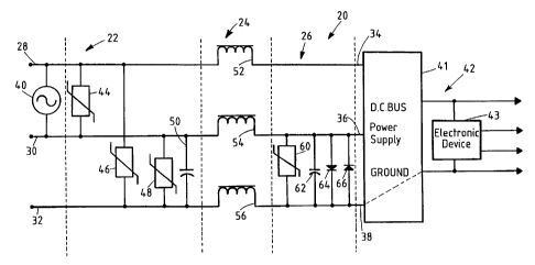
Referring first to Fig. 1, a power conditioning
circuit 20 having a set of first, second and third stages
22, 24 and 26 is connected between a set of line, neutral
and ground conductors 28, 30, 32 and a set of output lines
34, 36, 38. The line, neutral and ground conductors 28,
30, 32 may be connected to a commercial source of power 40
or any other power source. The first, second and third
stages 22, 24 and 26 are arranged such that power entering
the power conditioning circuit from the power source 40
first flows through the first stage, then through the
second stage and lastly the third stage. Upon exiting the
third stage, the power reaches the output lines 34, 36 and
38 which are connected to the load(s) 42. The load(s) 42
may include, for example, a power supply 41 that is coupled
to an electronic device 43, such as a computer.
The first stage 22 includes first, second and third
metal oxide varistors (MOVs) 44, 46 and 48 connected across
the line and neutral conductors 28, 30, the line and ground
conductors 28, 32 and the neutral and ground conductors 30,
32, respectively. In addition, a first capacitor 50 that
preferably, although not necessarily, has a rating of 25
microfarads is connected across the neutral and ground
conductors 30, 32.
The second stage 24 includes first, second and third
inductors 52, 54, 56 connected in series on each of the
line, neutral and ground conductors 28, 30 and 32,
CA 02394853 2002-06-05
WO 01/41278 PCT/US00/31199
-8-
respectively. The third stage 26 includes a fourth MOV 60
connected between neutral and ground conductors 30 and 32.
In addition, a second capacitor 62 is coupled between
neutral and ground conductors 30, 32 and first and second
rectifier diodes 64, 66 are connected in anti-parallel
relationship between the neutral and ground lines.
The first, second and third MOVs 44, 46, 48 of the
first stage 22 limit the voltage magnitudes appearing
across the line, neutral and ground conductors 28, 30, 32
by shunting currents during voltage spikes that exceed a
threshold voltage. It is preferable, although not
necessary, that the first, second and third MOV's each have
a rating of 150 volts RMS.
The first, second, and third inductors 52, 54 and 56
have rating values that attenuate transients having one or
more frequency components in excess of the nominal
frequency (typically 60 Hz) of the power supplied via the
line, neutral and ground conductors 22, 24, 26. It is
preferable, although not necessary, that the inductors 52,
54 and 56 each have the rating of 5 millihenries (mh).
The third stage 26 suppresses substantially all
undesired remaining energy components that are not diverted
or attenuated by the first and second stages 22, 24. More
particularly, the fourth MOV 60 limits the magnitude of the
voltages appearing on the neutral and/or ground conductors
and 32 by shunting currents to ground. Because any high
energy surges and high energy surge components have ideally
been filtered by the first and second stages, the elements
CA 02394853 2002-06-05
WO 01/41278 PCTIUSOO/31199
-9-
of the third stage need only be rated to divert or
attenuate lower energy surges. As a result, the MOV 60
preferably, although not necessarily, has a rating of 140
V RMS. Likewise, the second capacitor 62, which operates
to shunt power components having undesired frequencies to
the ground conductor 32, preferably, although not
necessarily, has a rating of 25 microfarads. The first and
second rectifier diodes 64 and 66 are connected in parallel
between the neutral and ground conductors 30, 32 such that
the polarity of the first rectifier diode 64 opposes the
polarity of the second rectifier diode 66. Arranging the
rectifier diodes 64, 66 in this manner enables precise, low
level voltage clamping, thereby further enabling voltage
control for the load ground. In applications wherein the
electronic device 43 of the load 42 is a computer, low
level voltage clamping on the ground leg is especially
advantageous because the ground lead attaches directly to
the microprocessor and is, therefore, a potential source of
damaging voltage spikes.
To provide power factor correction for a load having
a capacitive impedance characteristic, such as a computer,
and to thereby reduce power costs, the first, second and
third inductors 52, 54, 56 of the second stage are
preferably sized not only to dampen, or suppress high
frequency spikes, but also to offset the capacitive
impedance characteristics of the load. Thus, it is
preferable to employ inductors 52, 54 and 56 having rating
values that improve the overall power factor of the power
CA 02394853 2002-06-05
WO 01/41278 PCT/USOO/31199
-10-
supplied by the conditioning circuit to the capacitive
load, i.e., it is desirable to obtain a power factor that
approximates unity or comes as close thereto as practical.
The three stage power conditioning circuit described
herein provides high quality, precise and yet inexpensive
power conditioning. More particularly, by arranging the
first, second and third stages 22, 24, 26 in a cascaded
order such that the first and second stages 22 and 24
effect high energy suppression and isolation and the third
stage 26 effects low energy transient noise suppression,
less expensive circuit elements may be employed in each of
the three stages. The cost savings achieved by way of the
three stage power conditioning circuit of the present
invention are best understood with reference to the rating
of each of the circuit elements and a manufacturer
specified tolerance level associated with each of the
ratings. Specifically, the rating and tolerance level
associated with each circuit element affects the cost of
the circuit element such that circuit elements that are
rated for higher voltage levels and/or current levels are
typically more costly than circuit elements rated to handle
lower levels. In addition, a circuit element having a wide
tolerance associated with the rating is typically less
precise and therefore less costly than a circuit element
having a narrower, and thus, more precise tolerance
associated with the rating. In the three stage power
conditioning circuit of the present invention, the first
and second stages 22, 24 are used to suppress and/or
CA 02394853 2002-06-05
WO 01/41278 PCTIUSOO/31199
-11-
attenuate high energy transients and as a result the
circuit elements of the first and second stages 22, 24 are
preferably rated to handle these high energy surges.
However, because of the back-up protection provided by the
third stage 26, the circuit elements of the first and
second stages 22, 24 need not be particularly precise and
thus may have ratings with a wider tolerance level than
would otherwise be effective to adequately protect the
attached loads. Thus, the increased cost of providing
circuit elements in the first and second stages 22, 24 that
are capable of handling high energy surges is offset by the
wider tolerance levels associated with the ratings.
Conversely, because precise power conditioning is desired
at the third stage 26, circuit elements having narrower
tolerance levels are desirable. However, because the
circuit elements of the third stage 26 need only be rated
to perform low energy suppression/attenuation, the
increased cost associated with a narrower tolerance level
is offset by the decreased cost of the lower ratings
associated with the circuit elements of the third stage 26.
Referring now to Fig. 2, to provide enhanced noise
suppression, the second stage of the three stage power
conditioning circuit may be modified to include common mode
inductors 70, 72, 74 each having a first winding 70-1, 72-1
and 74-1 respectively, a second winding 70-2, 72-2 and 74-2
respectively, and a core 70-3, 72-3 and 74-3, respectively.
The first winding 70-1 of the common mode inductor 70 is
coupled in series with the first winding 74-1 of the common
CA 02394853 2002-06-05
WO 01/41278 PCT/US00/31199
-12-
mode inductor 74 between line conductor 28 and the first
output line 34, and the second winding 70-2 of the common
mode inductor 70 is coupled in series between the neutral
conductor 30 and the second output line 36. The second
windings 72-2 and 74-2 of the common mode inductors 72, 74
are coupled in series between the ground conductor 32 and
the third output line 38. The first and second windings
70-1 and 70-2 are wound on the core 70-3 while the first
and second windings 72-1 and 72-2 are wound on the core 72-
3 and the first and second windings 74-1 and 74-2 are wound
on the core 74-3. Each of the common mode inductors 70, 72
and 74 are arranged such that the polarity of the windings
of each of the inductors 70, 72 and 74 is identically
aligned as indicated by the polarity dots shown beside each
of the inductors 70, 72 and 74. By using common mode
inductors arranged in this manner, high frequency transient
voltages appearing across both the first and second
windings 70-1, 70-2, 72-1, 72-2, 74-1, 74-2 of the first,
second and third inductors 70, 72, and 74, respectively,
simultaneously act to cancel each other out, thereby
providing noise suppression.
Numerous modifications and alternative embodiments of
the present invention will be apparent to those skilled in
the art in view of the foregoing description. For example,
the third stage of the power conditioning circuit may
include an additional MOV (not shown) connected to the line
conductor at a point between the line conductor 28 and the
output line 34 and coupled between the line conductor 28
CA 02394853 2002-06-05
WO 01/41278 PCT/USOO/31199
-13-
and the neutral conductor 30 to protect against a high
power energy surge that reaches the third stage.
Accordingly, the description of the present invention
is to be construed as illustrative only and is for the
purpose of teaching those skilled in the art the best mode
of carrying out the invention. The details of the
structure and/or function may be varied substantially
without departing from the spirit of the invention, and the
exclusive use of all modifications which come within the
scope of the appended claims is reserved.