Note: Descriptions are shown in the official language in which they were submitted.
CA 02395281 2002-06-14
WO 01/50597 PCT/US00/34587
AUDIO COMPRESSION CIRCUIT AND METHOD
FIELD OF TI3E INVENTION
The present invention relates generally to compressor circuits for audio
signals. More particularly, the present invention relates to audio compressors
for
hearing aids.
BACKGROUND OF THE INVENTION
Audio compressors are devices that are commonly used to modify the
dynamic range of an audio signal. Generally, an audio compressor comprises an
amplifier and a control system to control the gain of the amplifier as a
function of the
input and/or output signal strength. An audio compressor circuit reduces the
gain of
an amplifier at high input signal levels to prevent distortion which would
otherwise
occur when the input signal exceeds a threshold Level. However, audio
compressors
also provide other useful benefits.
Commonly, an audio compressor is characterized in terms of a
compression ratio, which is the ratio of the gain at a reference signal level
divided by
the gain at a specified higher signal level. For example, an audio compressor
with a
3:1 compression ratio has the characteristic that each 3 dB increase in sound
level
beyond a threshold level results in a 1 dB increase in output. However, more
2 0 generally an audio compressor may be characterized in terms of a
compression
function that defines a relationship between input signal strength and the
differential
gain of the amplifier.
A variety of common sounds, such as the clang of a bell, have a sound
amplitude with a high initial amplitude which decays over time. It is
desirable that a
2 5 compressor reduce gain rapidly enough that the amplification of such
sounds does not
cause unpleasant distortion and/or an excessive sound-level. However, a highly
unnatural sound results if the gain recovers to its ordinary level too rapidly
after an
initial loud sound. Consequently, the transient response of a compressor has a
large
impact on the sound quality. Audio compressors are characterized in terms of
an
3 0 "attack" time, the time it takes for the amplifier to stabilize to within
about 1 dB of its
final increased value after a sudden increase in input audio level and a
"release" time
associated with the time it takes for an audio compressor to return to within
about 1
CA 02395281 2002-06-14
WO 01/50597 PCT/US00/34587
2
dB of its final decreased value after the input audio level has decreased to
normal
levels. Typically, it is desirable that an audio compressor have a release
time that is
much longer than its attack time. Typical release times are often in the range
of 1-10
milliseconds. Typical attack times are in the range of 0-1 milliseconds.
Audio compressors are commonly used in hearing aids. One reason
that audio compressors are used in hearing aids is that hearing loss is often
dependent
upon both the sound frequency and the audio level. The ability to hear,high
frequency
sounds may, for example, depend upon whether or not the listener is in a quiet
or
noisy environment. Typically less amplification is required if the background
audio
level is high. Thus, the required amplification will depend upon both the
sound
frequency and the audio level. An audio compressor that varies the
amplification as a
function of input audio level is thus useful for those types of hearing losses
for which
the input audio level determines the required amplification.
Audio compressors are also used in hearing aids to reduce distortion.
The human ear is very sensitive to harmonic distortion. As is well known in
the field
of amplifier design, there is typically a preferred range of input signal
levels for which
low-noise linear amplification is possible for a particular Class-A, Class-AB,
Class-
B, or Class-D amplifier circuit. An output amplifier that is driven close to
its
maximum power output typically produces substantial harmonic distortion as the
2 0 amplifier gain becomes saturated.
The design of an audio compressor for a miniature hearing aid is
constrained by several design considerations that are unique to miniature
hearing aids.
First, a miniature hearing aid is typically powered by a single miniature
hearing aid
battery, which provides a nominal 1.5 VDC and which is capable of only limited
load
2 5 currents. High performance microprocessor circuits, by way of comparison,
typically
operate at a voltage of 3.3 VDC. Second, total circuit size is a major concern
in the
design of a hearing aid, since modern miniature hearing aids are designed to
fit
partially or totally in the ear canal. Third, cost is an issue. While high
performance
hearing aids sell for several thousand dollars, there is a world-wide mass
market for
3 0 hearing aids with a price of less than about two-hundred dollars.
Moreover, since the
total cost to a user includes audiologist fees, it is desirable that the
characteristics of
CA 02395281 2002-06-14
WO 01/50597 PCT/US00/34587
3
the hearing aid may be quickly adjusted to accommodate the user's needs and
preferences.
Conventional audio compressors used in hearing aids commonly
comprise an op-amp amplifier circuit whose gain is controlled by a current-
controlled
resistor. FIG. 1 is a circuit schematic of a prior art hearing aid circuit. A
microphone
2 detects input sounds. An output amplifier stage 4 is used to provide large-
signal
amplification to provide an amplified signal to a speakerltransducer 6. A
small signal
amplifier and compression stage 8 includes an op-amp 16 with an input resistor
14
and a current-controlled resistor element 12. The compression function of
small
signal amplifier and compression stage 8 is achieved by gain control circuit
10
adjusting the resistance of current controlled resistor element 12 as a
function of the
audio signal input level. One common gain control circuit 10 uses the
logarithmic
current-voltage output of the collector-emitter current of a bipolar
transistor in
response to increasing base voltage in order to control the input currents to
current
controlled resistor element 12. However, there is only a limited current range
over
which a bipolar transistor has a current-voltage relationship that
approximates a
logarithmic function. Conventional current-controlled resistors also have
numerous
well-known limitations in regards to their accuracy and sensitivity.
There are several other drawbacks to the compressor circuit of FIG. 1,
2 0 particularly when the audio compressor stage 8, output stage 4 and other
electronics
(not shown in FIG. 1) are fabricated on one integrated circuit. Bipolar
transistors
require a substantial circuit area compared to complimentary metal oxide
semiconductor (CMOS) transistors. A hearing aid circuit fabricated using an
all
bipolar transistor process occupies a substantial circuit area, which
increases its cost.
Moreover, bipolar transistors consume more current and power than CMOS
transistor
circuits. While a mixed circuit fabrication process combining both CMOS
transistors
and bipolar transistors on one chip (commonly called a "bi-CMOS" process) is
technically feasible, a bi-CMOS fabrication process is typically expensive
compared
to fabricating either an all-bipolar or all-CMOS circuit.
3 0 The function of small signal amplifier and compression stage 8 may
also be implemented using a digital signal processing circuit (DSP). DSP
circuits
permit complex signal processing functions to be performed, permitting an
arbitrary
CA 02395281 2002-06-14
WO 01/50597 PCT/US00/34587
4
gain compression function to be achieved. However, DSP circuits typically
comprise
substantial memory, logic, and control circuit elements. A DSP circuit will
tend to
consume a substantial chip area and may draw a significant amount of current
compared to the hearing aid output amplifier stage 4. Generally, utilizing a
DSP
circuit to perform an audio compression function for the output amplifier
stage 4 of a
hearing aid would substantially increase the size, cost, and complexity of a
hearing
aid circuit.
Unfortunately, conventional audio compressor circuits used in hearing
aids tend to be expensive, requires a large area on an integrated circuit, and
suffer
from other problems, such as difficulties in providing control of audio
compression
over a wide range of audio input signal strengths. Moreover, most common audio
compressor circuits provide only a limited ability to control and select the
audio
compression function.
What is desired is a new compressor circuit design approach that
reduces the size, cost, and current requirements of an audio compressor
circuit
suitable for low voltage applications.
SUMMARY OF THE INVENTION
The present invention is generally directed towards an improved audio
compressor in which a rectified input voltage is used by an impedance
controller to
2 0 produce an impedance which is a stepwise function of the rectified
voltage. The
present invention generally includes an improved low voltage rectifier and an
impedance controller, which are preferably used together.
A preferred embodiment of the present invention generally comprises:
an amplifier; a switched charging state rectifier producing an rectified
voltage that is a
2 5 function of the magnitude of an input signal with a controlled transient
response, the
switched charging rectifier including: a capacitor; a charging switch coupling
the
capacitor to a charging node; a discharge switch coupling the capacitor to a
discharge
node; a switch controller adjusting the operation of the switches so that the
capacitor
is charged when the voltage on said capacitor is less than the magnitude of an
input
3 0 voltage and discharged when the voltage on said capacitor is greater than
the
magnitude of the input voltage; and a current limiting element coupled to the
discharging current path to limit the rate at which current may be discharged;
and an
CA 02395281 2002-06-14
WO 01/50597 PCT/US00/34587
impedance control circuit receiving as an input the rectified voltage of the
switched
charging state rectifier and providing a controlled impedance coupled to the
amplifier
to regulate the amplifier gain according to a compression function; wherein
the
capacitance of the capacitance and the electrical characteristics of said
current limiting
5 element are selected so that said compressor circuit has a preselected
release time.
One aspect of the present invention is a compact selector circuit to
convert the output of a rectifier into switch control signals to control an
impedance
selection circuit. In a preferred embodiment, a plurality of comparators whose
reference voltages are set by a resistor voltage divider are used to convert
the rectified
voltage into logical signals to control the operation of a plurality of
switches. In one
embodiment, the outputs of the comparator are used to control the switch
positions of
a resistor ladder. In another embodiment, the logical signals are used to
control the
operation of current sources in a current matrix, with the output current of
the current
matrix used to regulate an impedance.
One object of the present invention is to provide an audio compressor
with a controlled attacklrelease function.
Another object of the present invention is to provide an audio
compressor that permits a plurality of compression ratios or functions to be
selected.
Still another object of the present invention is to provide an audio
2 0 compressor that is comparatively inexpensive.
BRIEF DESCRIPTION OF THE DRAWINGS
FIG. 1 is a schematic circuit diagram of a prior art hearing aid with an
audio compressor
FIG. 2A is a block diagram of an audio compressor of the present
invention comprising a rectifier, an impedance controller, and an impedance
controlled amplifier.
FIG. 2B is an illustrative plot showing an impedance which is a
stepwise function of a rectified voltage.
FIG. 2C is a block diagram of an audio compressor of the present
invention comprising a time-sampling rectifier, amplifier impedance control
circuit,
and feedback amplifier with adjustable impedance element.
CA 02395281 2002-06-14
WO 01/50597 PCT/US00/34587
6
FIG. 3 is a schematic block circuit diagram of an embodiment of the
inventive audio compressor in which an impedance ladder used to control the
output
gain of an amplifier.
FIG. 4 is a schematic circuit diagram of an embodiment of the
inventive audio compressor in which the currents from a selector are summed to
provide a control current to adjust the output gain of an amplifier.
FIG. 5 is a block circuit diagram of an embodiment of the inventive
audio compressor in which a current-controlled impedance is used to adjust the
gain
of an amplifier.
FIG. 6 is a schematic circuit diagram of an embodiment of the
inventive audio compressor in which a switched capacitor element is used to
control
the gain of an amplifier.
FIG. 7 is a schematic circuit diagram of a second embodiment of the
inventive audio compressor in which a switched capacitor element is used to
control
the gain of an amplifier.
FIG. 8A is schematic circuit diagram of a first embodiment of switched
charging state rectifier of the present invention.
FIG. 8B is a schematic circuit diagram of a second embodiment of a
switched charging state rectifier of the present invention.
2 0 FIG. 9A is a schematic circuit diagram of a third embodiment of a
switched charging state rectifier of the present invention.
FIG. 9B is a schematic circuit diagram of a fourth embodiment of a
switched charging state rectifier of the present invention.
FIG. 9C is a schematic circuit diagram of a prior art current mirror.
2 5 FIG. 9D is a schematic circuit diagram of an inventive current mirror
circuit with an additional transistor switch coupled to the current mirror to
turn on and
off the mirror current.
FTG. ~ 0 is an illustrative plot of the output voltage of the inventive
switched charging state rectifier of FIG. 8A as measured in response to an
audio input
3 0 signal.
FIG. 11 is a fourth embodiment of the inventive switched charging
state rectifier designed to function at a nominal supply voltage of 1.2VDC.
CA 02395281 2002-06-14
WO 01/50597 PCT/US00/34587
7
FIG. 12 is an illustrative plot of the output voltage of the switched
charging state rectifier of FIG. 11 as measured in response to an audio input
signal.
FIG. 13 is a f fth embodiment of a switched charging state rectifier
configured to function as a full-wave rectifier.
FIG. 14 is a schematic circuit diagram of a selector circuit comprising
a plurality of comparators whose trigger voltages are controlled with a
voltage divider
circuit.
FIG. 15 shows three illustrative plots demonstrating how the trigger
voltages of the comparators of FIG. 14 may be selected to approximate various
mathematical functions by selecting the resistance values of the resistors
which are
part of a voltage divider.
FIG. 16A is a circuit schematic of a preferred embodiment of the
selector circuit of FIG. 14.
FIG. 16B is a circuit schematic of a preferred level shifter used in the
selector of FIG. 16A.
FIG. 17 is a schematic circuit diagram of a prior art op-amp feedback
amplifier.
FIG. 18 is a schematic circuit diagram of an op-amp feedback
amplifier in which one of the resistors is replaced by a resistor ladder whose
2 0 resistance may be selected by a plurality of switches.
FIG. 19 is a circuit schematic of a preferred embodiment of a resistor
ladder that utilizes the outputs of the selector of FIG. 18 to control the
switch
positions determining the resistance of the resistor ladder.
FIG. 20A is a block circuit diagram of a preferred embodiment of the
2 5 inventive compressor circuit incorporating a switched charging state
rectifier and
selector circuits to adjust the resistance of resistor ladder circuits
comprising part of
an op-amp amplifier.
FIG. 20B is a circuit diagram of a preferred adjustable feedback
resistor for use in the compressor circuit ofFIG. 20A.
3 0 FIG. 21 is a plot showing eight different compression functions that
may be achieved using the compressor circuit of FIG. 20A.
1i
~~y'so, a
CA 02395281 2002-06-14 ~ ..~w~"
$ - ~ . .. _
a
FIG. 22 is an illustrative schematic circuit diagram of a first
embodiment of a compressor circuit in which a switched capacitor is used to
control
the effective resistance of a portion of an op-amp feedback circuit.
FIG. 23 is a schematic circuit diagram of a bipolar circuit used to
control the switch frequency of the switched capacitor of FIG. 22.
FIG. 24 is a schematic circuit diagram of a selector circuit that converts
a rectified voltage into a control current used to control the switch
frequency of the
switched capacitor of FIG. 22.
FIG. 25 is a schematic circuit diagram of a preferred embodiment of the
switched capacitor amplifier of FIG. 22.
FIGS. 26A-26D are a schematic circuit of a preferred embodiment of a
complete audio compressor circuit utilizing switched capacitors.
DETAILED DESCRIPTION OF THE INVENTION
The present invention is directed towards audio compressors for hearing
aids, although more generally the present invention may be used in other
compressor
applications.
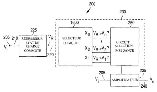
FIG. 2A shows a block diagram illustrating some of the general
principles of the present invention. A rectifier 100 produces an output
voltage that is a
function of the magnitude of an input voltage. In a preferred embodiment, the
transient characteristics of rectifier 100 (i.e., its characteristic rise and
fall response
time to changes in the magnitude of the input voltage) are preselected. As
described
below in more detail, the inventors have developed an extremely sensitive low
voltage
rectifier which permits small decibel changes in input voltage level (i.e.,
sound level)
to be resolved.
The output of rectifier 100 is coupled to an impedance controller 110.
Impedance
controller 110 has an output impedance that is a preselected stepwise function
of the
rectified voltage. As described below in more detail, in a preferred
embodiment
impedance controller 110 incorporates digital circuit elements which switch
(i.e, adjust
in steps) the output impedance as a function of the rectified voltage.
The output impedance of impedance controller 110 is used to regulate
the gain of an amplifier 120. Amplifier 120 may be any type of amplifier that
has an
output gain which is a function of an impedance, such as a feedback amplifier.
FIG.
Substitute Sheet
,,
CA 02395281 2002-06-14
WO 01/50597 PCT/US00/34587
9
2B is an illustrative plot showing an output impedance, z, that is a stepwise
function
of the rectified voltage, Vr. By appropriate selection of the stepwise output
impedance, z, of impedance controller 110 the output of amplifier 120 will
approximate a continuous compression function, i.e., be a piecewise linear
approximation of a continuously varying compression function. The inventor has
recognized that for audio applications the compression function will
approximate a
continuous function to the human ear if the separation between compression
steps is
less than about one dB. For example, to approximate a compression function
which
smoothly varies over 40 dB impedance controller 110 should produce an
impedance
function that is a stepwise function of the rectified voltage with at least 40
steps. It
will also be understood that the requirements of rectifier 100 will also
depend upon
the required number of steps and the voltage range of the input voltage, i.e.,
upon the
smallest voltage that must be revolved.
The preferred embodiments of the present invention generally
l 5 comprise three main aspects. One aspect of the present application is a
switched
charging state rectifier 225 which is a novel rectification circuit that is
extremely
sensitive and which has a controllable transient response. In quasi-steady
state
operation, the magnitude of the output voltage 220 of switched charging state
rectifier
tracks the magnitude of the input voltage 210. However, if the input voltage
rapidly
2 0 changes in magnitude, the magnitude of the output voltage 220 of switched
charging
state rectifier has a characteristic transient rise/fall response. For
example, in order to
achieve a release time of five milliseconds, the output 220 should decay in
response to
a decrease in magnitude of the input signal 210 at a rate such that output 220
decays
in five milliseconds to a value close to its final value (e.g., within one dB
of its final
25 value). FIG. 2C shows, in phantom, a generalized impedance control circuit
230
which converts a rectified voltage 220 into a controlled impedance which
regulates
the gain of an amplifier 235. Impedance control circuit 230 may be an
conventional
circuit that performs the function of converting a voltage into an impedance.
However, conventional impedance control circuits 230 have a limited
sensitivity
3 0 and/or other drawbacks.
A second aspect of the present invention is a preferred inventive
selector circuit 1600 to convert the rectified voltage 220 of switched
charging state
CA 02395281 2002-06-14
WO 01/50597 PCT/US00/34587
rectifier 225 into switch control signals to regulate the impedance of an
impedance
selection circuit 250 whose impedance may be selected by opening/closing a
plurality
of switches. All of the preferred embodiments of the present invention utilize
a
selector 1600 in combination with an impedance selection circuit since this
provides
5 superior control over an impedance to regulate the gain of an amplifier 235.
A third aspect of the present invention are compact, low-voltage
impedance selection circuits designed to convert the selector outputs into an
impedance that varies with signal strength according to a compression
function.
Preferred impedance control circuits include a switched resistor ladder and a
switched
10 current matrix.
Block schematic diagrams of various embodiments of an audio
compressor 200 of the present invention are shown in FIGS. 2C-7. FIG. 2C shows
the
general block diagram of an audio compressor 200 of the present invention. A
switched charging state rectifier 225 has an output 220 that is input into an
impedance
control circuit 230 which regulates the gain of an amplifier 235. As shown in
FIG. 2,
an input signal 205 enters audio compressor 200. A portion of input signal 205
is fed
into input node 210 of switched charging state rectifier 225. Amplifier 235
also
receives as an input signal 205. Input signal 205 may be supplied directly by
a
microphone but is preferably supplied in conjunction with well-known isolation
and
2 0 small-signal amplification elements. Impedance control circuit 230 may be
implemented in a variety of ways, as indicated in FIGS. 3-7. Amplifier 235 may
be
any amplifier whose gain can be regulated by an impedance, but is preferably
an op-
amp feedback amplifier whose gain may be regulated by a variable resistance.
Switched charging state rectifier 225, which is shown in detail in
FIGS. 8-I3, is a device that produces an output that is a function ofthe
magnitude of
the input signal. Unlike an ideal rectifier, switched charging state rectifier
225 has a
controllable transient response, implemented in the form of a selectable
release
function and/or attack function. Switched charging state rectifier 225
operates on the
principle of comparing the magnitude of the input voltage to the voltage on a
capacitor and making a logical decision to charge/discharge the capacitor. The
charging and discharging current paths are selected so that the
charging/discharging
CA 02395281 2002-06-14
WO 01/50597 PCT/US00/34587
11
response of the capacitor produces an output voltage on the capacitor that
increases/decreases in time according to a predetermined transient response
function.
Switched charging state rectifier 225 produces an output that includes a
preselected transient release/attack function. Since the time response is
included in
rectified voltage 220, a compression function that includes an attack/release
response
is achieved by coupling output voltage 220 to an impedance control circuit 230
to
convert rectified voltage 220 into an impedance. Switched charging state
rectifier 225
also has exceptional resolution, and can distinguish voltage differences of
less than
250 micro-volts, which is desirable if the output voltage 220 is to be used to
determine a gain compression function over a range of audio input levels. In
particular, the sensitivity of switched charging state rectifier 225 permits a
an input
signal of less than about one volt to be resolved into a plurality of steps
each
corresponding to a less than one dB change in input signal.
FIG. 3 shows an embodiment of the audio compressor of FIG. 2 for
which a preferred implementation is described in more detail with respect to
FIGS.
17-21. A switched charging state rectifier 225 provides a rectified voltage
output 220
that is input to a selector 1600. Selector 1600 provides a plurality of
comparator
outputs Xl, X2, . . . XN, each of which has a pre-selected trigger voltage
coupled to
switches S1, S2, . . . SN of impedance ladder 1510. Impedance elements 2220
are
2 0 preferably resistors arranged in accord with any parallel or series
resistor ladder
configuration in which the effective resistance of the impedance ladder 1510
depends
upon which of switches S1, S2, . . . SN are in a conducting or non-conducting
state.
The individual switches Si, S2, . . . SN of impedance ladder 1510 may be of
any type,
but are shown as comprising n-channel MOSFET transistors. Impedance ladder
1510
provides an impedance, Z, to amplifier 235, whose impedance is controlled by
switches S1, S2, . . . SN. Amplifier 235 may be any kind of amplifier whose
gain may
be controlled by varying an impedance, Z, but is preferably an op-amp feedback
amplifier in which the resistance ladder determines the gain. Preferably the
number
of logical outputs is selected so that the resistance of the impedance ladder
1510 may
3 0 be incrementally adjusted as a function of rectified voltage 220 so that a
variety of
quasi-continuous compression functions may be approximated to a high degree of
accuracy (e.g., step-changes in the resistance of the impedance ladder 1510
may be
CA 02395281 2002-06-14
WO 01/50597 PCT/US00/34587
12
triggered by one dB changes in input signal strength to approximate linear,
logarithmic, or other gain compression functions).
Logical selector 1600 provides logical outputs to control an impedance
selector 250. A preferred logical selector 1600 comprising a plurality
comparators in
which each comparator has its reference voltage determined by a resistive
voltage
divider is shown in more detail in FIGS. 14-16. Logical selector 1600
preferably
provides output control signals which are a logical function of the rectified
voltage
220. In a preferred embodiment, each output, Xl . . . XN of logical selector
1600
corresponds to the single binary output for the logical function, is VR>V;,?
where VR
is the rectified voltage 220 and V; is a reference voltage for output X;. The
logical
outputs of logical selector 1600 are input to an impedance selector 250, which
selects
an appropriate impedance to regulate the gain of amplifier 235 according to a
compression function.
The preferred embodiment shown in FIG. 3 is what the inventor
describes as a "mixed signal" circuit application. An analog signal from
switched
charging state rectifier 225 is converted info logical switch position
decisions by
logical selector 1600. The switch positions S1 . . . SN of resistor ladder
1510 are used
to determine the resistance of resistor ladder 1510 so that it regulates the
gain of
analog amplifier 235 according to a compression function. This mixed signal
2 0 application provides the benefit of improved control over the audio
compression
function because the logical selector 1600 and resistor ladder 1510 can be
used to
achieve a preselected compression function in which the gain varies with input
signal
magnitude according to any quasi-continuous function.
The sensitivity and resolution of switched charging state rectifier 225
2 5 is an important part of the present invention which permits the
implementation of the
embodiment of FIG. 3. However, since the sensitivity of conventional low-
voltage
rectifiers continues to improve, the function of switched charging state
rectifier could
be emulated by a sensitive low-voltage rectifier (i.e., one capable of
resolving an
audio input signal to less than one dB increments) coupled to other elements
to
3 0 achieve a rectified voltage with a selectable attack/release function
(e.g., a passive
arrangement of capacitors and resistors).
CA 02395281 2002-06-14
WO 01/50597 PCT/US00/34587
13
FIG. 4 shows a second embodiment of the audio compressor circuit of
FIG. 2. As shown in FIG. 4, the rectified voltage 220 from switched charging
state
rectifier 225 is input to a selector 1600. Selector 1600 provides a plurality
of
comparator outputs Xl, XZ, . . . XN, each of which has a pre-selected trigger
voltage.
The outputs Xl, X2, . . . XN of selector 1600 are preferably used to select
which
constant current sources 2405 of current matrix element 2400 are turned on in
order to
adjust the magnitude of a control current, i~. The control current, i~, is
used to control
the impedance of a current-controlled impedance element 260 of an amplifier
235.
Current-controlled impedance element 260 may be any conventional current-
controlled impedance element, such as a current controlled resistor.
Preferably,
control current, i~, may be varied in small enough steps so that the amplifier
235 gain
may be regulated in a manner to implement a quasi-continuous compression
function.
FIG. 5 shows a third preferred embodiment of an audio compressor. In
the embodiment of FIG. 5, the rectified output 220 of switched charging state
rectifier
225 is input to any conventional voltage to current converter 255. The output
of
voltage to current converter 255 is then input to a current controlled
impedance
element 260 of an amplifier 235.
FIG. 6 shows a fourth embodiment of an audio compressor, a preferred
implementation of which is shown in more detail in FIGS. 22-26. The embodiment
of
2 0 FIG. 6 is similar to that of FIG. 4 in that it utilizes a logical selector
1600 to select
which current sources 2405 of current matrix 2400 are enabled in order to
adjust a
control current i~. However, in the embodiment of FIG. 6, the control current
i~ is fed
into a current-controlled oscillator (clock) 270 whose frequency is a function
of an
input current. The output of oscillator 270 is used to control the operation
of a switch
S, Which is in series with a capacitor, C, coupled to amplifier 235 as a
switched
capacitor element. The switched capacitor has an average resistance governed
by the
switching frequency so that the effective resistance of the switched capacitor
is
determined by the frequency of oscillator 270.
FIG. 7 is a fifth embodiment of an audio compressor, similar to that of
3 0 FIG. 6, except that a conventional voltage-to-current converter 255 is
used to convert
the rectified voltage 220 of switched charging state rectifier 225 into a
control current.
As in the embodiment of FIG. 6, the control current is used to determine the
switching
CA 02395281 2002-06-14
WO 01/50597 PCT/US00/34587
14
frequency of a switched capacitor element via oscillator 270, thus permitting
the gain
of amplifier 235 to be controlled. Voltage-to-current converter 255 may
comprise any
conventional voltage-to-current converter but is preferably a bipolar
transistor.
FIGS. 8-13: SWITCHED CHARGING STATE RECTIFIER
FIGS. 8-13 show various embodiments of the switched charging state
rectifier 220. Some of these embodiments are, for the purposes of teaching the
present invention, half wave rectifiers. However, it will be recognized by
those of
ordinary skill in the art that full-wave embodiments are preferred for audio
applications. It will also be recognized by those of ordinary skill in the art
that
compact, low-voltage embodiments are preferred for miniature hearing aid
applications.
FIG. 8A shows an illustrative circuit diagram of one embodiment of an
inventive switched charging state rectifier 800. This embodiment, which is
preferred
in some low-cost hearing aid applications, provides an output that follows
changes in
the magnitude of the input signal 805 but which has a controlled release
function.
Op-amp 845 is preferably arranged in a so-called, "voltage follower
configuration
with op-amp output terminal 865 coupled on the inverting input terminal 860.
In a
voltage follower configuration, the voltage at op-amp input terminals 855, 860
is
identical so that the voltage at node 850, op-amp output terminal 865, and
node 870
2 0 (which is coupled to input terminal 860) are equal to one another. Since
capacitor 830
is coupled to input terminal 855 of op-amp 855, the voltage on nodes 850 and
870 is
identical to that of capacitor 830.
When charging switch 825 is closed and a discharge switch 840 is
open, capacitor 830 is coupled to charging node 806 so that the voltage on
capacitor
2 5 830 raised to the input voltage level 805 with a time constant limited
only by the RC
time constant of charging switch 825 and capacitor 830. When charging switch
825 is
open and discharge switch 840 is closed, discharge current node 836 is coupled
to
capacitor 830 so that discharge current source discharges (e.g., sinks) the
charge on
capacitor 830, thereby reducing the voltage on capacitor 830.
3 0 The voltage on a capacitor is given by the expression: V=Q/C, where
V is the capacitor voltage, Q is the charge, and C is the capacitance. The
rate at
which the voltage decreases is given by the expression: dV/dT=1/C(dQ/dT).
Since
CA 02395281 2002-06-14
WO 01/50597 PCT/US00/34587
current source 835 determines the rate at which current discharges from
capacitor
830, this can be expressed as: dV/dT=I/C, where I is the current of current
source 835.
The rate at which the voltage decreases can thus be selected by appropriate
choice of
C, I. Current source 835 may comprise any conventional current source.
However,
5 current mirrors, in particular, are a preferred current source because the
current of a
CMOS current can be precisely selected over a wide range of values. Moreover,
by
selecting a current mirror with a low-current, I, the capacitance can be
correspondingly reduced, which permits capacitor 830 to be implemented as an
integrated capacitor.
10 The opening and closing of shunt charging switch 825 and discharge
switch 840 are controlled by a switch control logic element 815. Switch
control logic
element 815 has as a first input the input signal 805. Switch control logic
element
815 has as a second input the voltage at capacitor 830 (which is equal to the
voltage at
input terminal 855 and the rectified output voltage 870). Additionally, switch
control
15 logic element 815 preferably has a third input signal corresponding to a
clock signal
810 from a clock source (not shown in FIG. 8A). Clock signals 810 facilitate
switch
control logic element 815 periodically sampling the input voltage 805,
comparing it to
the rectified voltage 870, and making a decision on the proper switch position
of
discharge switch 840 and shunt switch 825.
2 0 There are two operating states of the switched charging state rectifier
800 of FIG. 8 when switch control logic element 815 is enabled by clock
signals 810.
In a first state, the input voltage 805 is increasing. In this first state,
S1, switch control
logic element 815 acts to close charging switch 825 and to open discharge
switch 840.
This results in the output voltage 850 and the voltage on capacitor 830
increasing to
2 5 the new level of input voltage 805. In a second state, S2, the input
voltage 805 is
decreasing. In this second state, switch contra( logic element 815 acts to
close
discharge switch 840 and to open charging switch 825. This results in the
voltage on
capacitor 830 decreasing at a rate that depends upon the magnitude of the
current of
current source 835. Switch control logic element 815 preferably makes
decisions to
3 0 change the operating state of the switched charging state rectifier 800 in
accord with
clock signals 810 (e.g., the clock signals enable switch control logic element
815 to
make decisions on changing the switch positions). The function of the switched
CA 02395281 2002-06-14
WO 01/50597 PCT/US00/34587
16
charging state rectifier 800 of FIG. 8 is summarized in
Table I.
INPUT SIGNAL SWITCHES OUTPUT VOLTAGE
CONDITION WHEN
CONTROL UNIT
ENABLED
Input Voltage 805 Charging Switch Output Voltage 870
Greater Closed;
Than Or Equal To Discharge Switch Increases To Increased
Output Open
Voltage 870 Level of Input Voltage
Input Voltage 805 Charging Switch Output Voltage Decreases
Less Open;
Than Output Voltage Discharge Switch At A Rate Determined
870 Closed By
Capacitance of Capacitor
and Magnitude of The
Discharging Current
TABLE I. Summary of the function of the inventive switched charging state
rectifier
of FIG. 8A.
While a constant current source 835 is a preferred implementation, the
discharge current may also be determined by a non-constant current discharge
path.
FIG. 8B shows an embodiment in which current source 835 is replaced with a
discharge resistor 837. In the context of compact hearing aids, this
embodiment is
less desirable because a discharge resistor 837 with a sufficiently large
resistance to
produce an RC time constant on the order of milliseconds with an integrated
capacitor
(i.e., a resistance on the order of at least several MegaOhms) would require a
discrete
resistor.
The switched charging state rectifier 800 of FIG. 8A has an extremely
short attack time, which is acceptable in many applications, such as in a low-
cost
compressor circuit. However, in some applications it is desirable to be able
to further
control the attack time. Variations of the switched charging state rectifier
embodiment of FIG. 8A, are the subject of another patent application of the
assignee
2 0 of the present invention, "Multiple Time Constant Rectifier," Attorney
Docket
6454/53821. "Multiple Time Constant Rectifier," Attorney Docket 6454/53821,
the
teachings ofwhich are hereby incorporated by reference, is being filed the
same day
as the present application. As shown in FIG. 8C, one of the variations
described in
CA 02395281 2002-06-14
WO 01/50597 PCT/US00/34587
17
more detail in "Multiple Time Constant Rectifier" is the modification of the
switched
charging state rectifier of FIG. 8A to include a constant current source 827
to control
the attack time of switched charging state rectifier 800. In the embodiment of
FIG.
8C, switch control logic closes charging switch 825 and opens discharge switch
840
when the magnitude of the input signal is greater than the voltage on
capacitor 830.
Consequently, current will flow from charging node 826 to capacitor 830. The
charging current will increase the capacitor voltage at a rate determined by
the
magnitude of the current of current source 827 divided by the capacitance of
capacitor
830. As discussed before in regards to FIG. 8A, when the magnitude of the
input
signal 805 is less than the voltage on capacitor 830, charging switch 825 is
open and
discharge switch 840 closes, resulting in the voltage on capacitor 830
decreasing at a
rate determined by the magnitude of the current of current source 835 divided
by the
capacitance of capacitor 830.
The switch control logic element 815 of FIG. 8A may be implemented
in a variety of ways. However, as shown in FIG. 9A, a preferred apparatus
using a
minimum number of circuit elements is to use a combination of comparators,
data
flip-flops, logic gates, and drivers. Switched charging state rectifier 900
uses a
comparator 975 and a clocked data flip flop 980 to control the operation of
the
discharge MOSFET switch 840 and charging MOSFET switch 825. For low voltage
2 0 operation, a high voltage driver 944 is preferably used to reduce the on-
resistance of
charging switch 825. A high voltage driver 944, such as a voltage doubter,
also
permits switch 825 to be dimensioned small enough to reduce parasitic charge
injection effects. In accord with well-known principles of data flip-flop
operation,
changes in output state of data flip-flop 980 will only occur when data flip-
flop 980 is
2 5 enabled by clock signals to an input port E. Thus, clocked data flip-flop
980 will
accept inputs from the comparator 975 and make logical decisions on a periodic
basis,
with the period governed by the frequency of clock signals entering the "E"
port of
clocked data flip-flop 980.
As indicated in FIG. 9A, charging switch 825 is coupled to one of the
3 0 outputs of data flip-flop 880 by a high voltage driver 944. High voltage
driver 944
may comprise any combination of static or dynamic voltage multipliers
configured to
provide a drive voltage sufficient to drive charging switch 825 well into the
ohmic
CA 02395281 2002-06-14
WO 01/50597 PCT/US00/34587
18
region, to reduce the on-resistance of the switch, and permitting its gate
width to be
comparatively narrow (e.g., less than about five microns) to reduce the
effects of
parasitic charge injection and capacitive feedthrough in the operation of the
circuit.
Discharge switch 840 is coupled to the other (complementary) output of data
flip-flop
980. As can be seen in FIG. 9A, whenever the rectified voltage 870 is higher
than the
input voltage 805, a high signal will enter the "D" port of flip-flop 975 from
the
output 977 of comparator 975. Consequently, the first output, Ql, of data flip
flop
980 coupled to the gate of switch 825 will be high, turning charging switch
825 on.
The second (complementary) output, Q2, of data flip flop 880 is coupled to the
gate of
discharge switch 840. Since QZ is the complement of the first output Ql, Qz is
low
and discharge switch 840 will be open. When the input voltage 805 on
comparator
975 begins to decrease, the outputs of the data flip flop 980 will change so
that Qi is
low and Q2 is high, shutting off shunt switch 925 and closing discharge switch
940.
FIG. 9B shows an embodiment of logical control element 815 for the
embodiment of FIG. 8C. MOSFET charging switch 825, however, couples capacitor
830 to a current source 827. While FIGS. 9A and 9B show embodiments with
constant current sources 835, 827, more generally non-constant current sources
could
be used as well. Moreover, while it is desirable for many hearing aid
application that
the current source (constant or non-constant) be selected to achieve an
attack/release
2 0 time on the order of at least one millisecond, a circuit designer may
select the
attack/release times as desired. In some applications, for example, it may be
desirable
to have a comparatively high discharge current so that switched charging state
rectifier emulates the response of an ideal rectifier (i.e., negligible
attack/release time
constants).
Referring again to FIGS. 8A and 8C, switched current sources are
utilized in preferred embodiments of the switched charging state rectifier to
control
the release function and/or attack function. The inventor has developed a
switched
current mirror which may be used to perform this function. A conventional
current
mirror is shown in FIG. 9C. In a MOSFET current mirror, the gates of two
MOSFETS are coupled together. The first MOSFET M1 is a diode-connected-
transistor, i.e., its drain and gate are electrically connected. A reference
bias current,
IDI, flowing through the source-drain terminals of diode-connected-transistor
Ml
CA 02395281 2002-06-14
WO 01/50597 PCT/US00/34587
19
determines the mirror current in the second MOSFET MZ because the bias voltage
on
the gate of transistor M2 is determined by the voltage coupled by diode-
connected-
transistor M1. The reference bias current IDI, is supplied by another current
source.
The mirror current, IDZ is a multiplicative factor of the reference bias
current, IDI, with
the multiplicative factor depending upon the relative sizes (e.g., gate width)
of
transistors M1 and M2. Any conventional current mirror whose current output
may
be regulated using another switch may be used as part of a charging current
element
or discharging current element of the present invention. FIG. 9D shows a
preferred
embodiment of a switched current-mirror. A switch M3 has its source and drain
terminals coupled to those of transistor M1. When switch M3 is turned on, it
will
shunt reference bias current ID1 from transistor M1, which turns off the
mirror current
of transistor M2 (which is a multiplicative factor of the current flowing in
transistor
M1). Thus, a current mirror may be used to perform the function of a current
source
827, 835 with switch M3 performing the function of a switch 825,840 to turn
on/off
the mirror current. The selection of reference bias current IDl and the
relative sizes of
transistors M1 and M2 may be used to create a current source with a very small
and
accurately controlled current value. This permits the charging and discharging
currents to be selected to achieve a wide range of charging/discharging rates
of
capacitor 230.
2 0 FIG. 10 is an illustrative plot of output voltage versus input voltage for
the inventive switched charging state rectifier 900 of FIG. 9A. In a first
time interval,
Tl, the input voltage 1010 is rapidly increasing so that the switched charging
state
rectifier 900 functions in the first state, S1, with the charging switch 825
closed and
discharge switch 840 open. Conseduently, the output voltage 1030 tracks the
input
voltage 1010 to peak 1015. In a second time interval T2, input signal 1010 is
decreasing, and the circuit switches to the second operating state, S2, with
shunt
switch 825 open and discharge switch 840 closed. The output voltage 830
decreases
according to an discharge time constant governed by the rate at which
discharge
switch 840 permits current to leave capacitor 830. At the beginning of a third
time
3 0 interval T3, the input voltage 1010 begins to exceed the output voltage so
that the
circuit switches back to the first operational state, causing the output
signal 1030 to
again track the input voltage 1010 to peak 1035. At the beginning of a fourth
time
CA 02395281 2002-06-14
WO 01/50597 PCT/US00/34587
interval T4, input signal 10.10 begins to decrease, so that the circuit
switches back into
the second operational state.
A preferred embodiment of a low-voltage switched charging state
rectifier 225 utilizing a current mirror as a constant current source 835 and
a high
5 voltage driver 944 is shown in FIG. 11. Charging switch 825 is preferably an
n-
channel MOSFET transistor, since n-channel MOSFETs have a higher conductance
per unit of gate width compared with p-channel MOSFETs. A transient voltage
pulse doubter 1180 is used as part of a high voltage drive 944 (shown in FIG.
9A) to
increase the voltage of control signals 1182 supplied to the gate of charging
switch
10 825 to greater than about 1.8 volts. A variety of voltage doubters are
known in the
prior art. However, the transient voltage pulse doubter 1180 shown in FIG. 11
is
preferred because of its compactness and efficiency. A transient voltage pulse
doubter for increasing the voltage to the switches of a Class-D power
amplifier is
described in U. S. Pat. App. Ser. No. 09/149,257 of the assignee of the
present
15 invention, the teachings of which are hereby incorporated by reference. A
compact
transient voltage pulse doubter for increasing the voltage of a small number
of
switches is described in the patent application of the assignee of the present
inventon,
"Switched Capacitor Filter With Integrated Voltage Multiplier," Attorney
Docket
6454/53786, which is being filed the same day as the present application. The
2 0 teachings of "Switched Capacitor Filter With Integrated Voltage
Multiplier," are also
hereby incorporated by reference. As indicated in FIG. 11, a voltage
multiplier 1120
is also preferably used to generate voltage multiplied control signals for the
operation
of switch 982.
As shown in FIG. 11, a current mirror is preferably used to control the
discharge current. Transistors MN2 and MN3 comprise a portion of a current
mirror
which is turned on/off by transistor MN4. A reference current source is
omitted for
the purposes of clarity in FIG. 11. However, any low-current reference current
source
may be coupled to line IMNO 1 C to complete the current mirror in the manner
shown
in FIG. 9D. When the voltage on the gate of MOSFET MN4 is high, transistor MN4
3 0 is switched on, which results in a low (e.g., zero) gate voltage on MOSFET
MN2
corresponding to an open circuit. However, if the voltage on the gate of
MOSFET
MN4 is low, MOSFET MN4 is substantially non-conducting and the gate voltage on
CA 02395281 2002-06-14
WO 01/50597 PCT/US00/34587
21
the gate of transistor MN2 will rise to a level determined by the reference
current
flowing in transistor MN3 so that, MOSFET MN2 will conduct a mirror current.
Comparator 975 sense changes between the rectified voltage 855 and
the input voltage 805. A high performance comparator can sense extremely small
voltage differentials on the order of micro-volts. Transistors 982 is coupled
to NOR.
gates 1102,1104 and inverter 1106 to form a clocked data flip flop. The first
output
1178 of data flip flop 980 drives the gate of transistor MN4 of low voltage
driver 942.
The second complementary output 1182 of data flip flop 980 is used to control
the
operation of shunt switch 825 As can be seen in FIG. 11, second complementary
output 1182 of data flip flop 980 is input to a NOR logic gate 1186 along with
an
inverted clock signal PHB. An inverter 1188 is used to invert the output of
NOR gate
796 prior to transient pulse voltage multiplier 1180, with the output of
transient pulse
voltage multiplier 1180 driving the gate of shunt charging transistor 825.
The circuit of FIG. 11 has two operational states. The first operational
l 5 state corresponds to the input voltage being greater than or equal to the
rectified
voltage. When the input voltage 805 exceeds the rectified voltage 870, the
output of
comparator 975 is low. First output I 178 of data flip flop 980 will be high,
so that
transistor MN4 will turn off the current mirror comprises of transistor MN2
and
MN3 The second output 1182 of data flip flop 980 will be low, which results in
a high
2 0 output 1182 from transient pulse voltage multiplier 1180, which turns on
shunt switch
825. Charging switch 825 is turned on, and the rectified voltage 870 follows
the input
voltage in accord with the principles of a voltage follower op-amp circuit.
The
second operational state is for the case the input voltage is less than the
rectified
voltage. When the input voltage 805 is less than the rectified voltage 870,
comparator
2 5 890 produces a high output to data flip-flop 790. Second output 1182 of
data flip-flop
790 will be high whereas first output 1178 of data flip-flop 980 will be low.
A low
value of first output 1178 resulting in transistor MN4 turning on the current
mirror
comprising transistors MN2 and MN3, discharging the capacitor. The
corresponding
high value of second output 1182 results in a low output voltage of transient
voltage
3 0 multiplier 1180 so that charging transistor 825 is an open switch. The
rectified
voltage 870 will, in accord with the principles of a voltage follower,
decrease as
current is discharged from capacitor 830 by the mirror current of transistor
MN2.
CA 02395281 2002-06-14
WO 01/50597 PCT/US00/34587
22
This state will continue until the voltage on capacitor 830 decays to the
level of the
input voltage 805.
FIG. 12 shows an illustrative plot of an input voltage 810 and its
corresponding output voltage 820 for switched charging state rectifier 1 I00
as a
function of time. Additionally, corresponding voltages at the output E of
comparator
790, the output voltages 1178, 1182 of data flip-flop 798, and the output A of
transient pulse voltage multiplier 780 are shown.
FIG. 13 shows a preferred embodiment of a full-wave switched
charging state rectifier 1300 suitable far use as part of the present
invention. The
function of the key circuit sub-blocks has been already described in regards
to the
embodiment of FIG.11. In order to achieve full-wave rectification, an
additional op-
amp configured as a voltage inverter is used so that the rectified voltage may
be
compared to the inverted input voltage whenever the voltage has a negative
sign.
In order to compare the inverted voltage with the capacitor, the other
comparison and decision circuits previously described are required. Thus, the
embodiment of FIG. 13 requires the additional elements of a voltage inverter;
second
shunt charging switch to coupled the inverted voltage input to the capacitor;
a second
comparator coupled to the rectified voltage and the inverted voltage input; a
second
data flip-flop configured to provide control signals to run on the second
shunt switch;
2 0 and a second high voltage driver to increase the strength of drive signals
to the second
shunt charging switch.
Calculations by the inventor indicate that switched charging state
rectifier 1100 can sense input voltage changes at least as small as 250 p,V
and perhaps
as low as 10 p,V. The ultimate limit on the sensitivity of the switched
charging state
rectifier is limited by the sensitivity of the comparators. The ability of
switched
charging state rectifier 225 to resolve small differences in the magnitude of
an input
signal 205 permits switched charging state rectifier 225 to distinguish small
variations
in the power of the input signal to a hearing aid, such as a change from an
input signal
level of 50 dB to 51 dB. No conventional low-voltage rectifier has a
comparable
3 0 sensitivity and resolution
FIGS. 14-16: PREFERRED SELECTOR CIRCUIT
CA 02395281 2002-06-14
WO 01/50597 PCT/US00/34587
23
Referring back to FIG. 2C, a selector 1600 is preferably used to
convert a rectifier voltage 220 from switched charging state rectifier 225
into control
signals for an impedance selection circuit 250 whose impedance is controlled
by a
plurality of switches. The function of logical selector 1600 could be
performed using
an A-D converter and other memory and control elements. However, the inventors
have developed an extremely compact selector 1600 that reduces the circuit
area
which would otherwise be required to implement the same function.
Selector 1600 preferably comprises a total ofN comparators 1610,
where N is an integer greater than one. One input to each comparator 1610
comprises
the rectified voltage 220 from the switched charging state rectifier 225. The
other
input to each comparator 1610 is the voltage from a voltage divider network
1620
comprising at least N resistors connected in series to a reference voltage,
Vref. As
indicated in FIG. 14, each comparator 1610-i, has an associated resistor, R;.
The
resistance of each resistor RI, RZ, . . . RN is selected so that the voltage
at each
resistor, Vl, VZ, . . . VN , is used as a reference voltage for comparators
1610-l, 1610-
2, . . . 1610-N.
Reference voltages, Vl, V2, . . . VN may be related to one another
according to a variety of mathematical relationships which may be implemented
by
appropriate selection of the values of resistors Rl, R2, . . . RN. Modern
integrated
2 0 circuit fabrication techniques permit thevalues of the resistance of each
resistor to be
selected over a wide range (e.g., over a range between 1 kilo-Ohm to over one-
hundred kilo-Ohms). The output voltage along a voltage divider 1310 can be
readily
calculated from well-known voltage divider expressions. By appropriate
selection of
the values of each resistor, Rl, Rz, . . . RN, the values of Vl, VZ, . . . VN
may be
2 5 selected to be a pre-calculated fraction of V,.~f based upon the ratio of
the sum of the
resistances connecting a given comparator input to ground divided by the total
resistance in the chain, which can be expressed mathematically for the ith
resistor as:
~1-Vref ERi/ER. Since the trigger voltage depends upon a ratio of resistances,
it is
independent of lot-to-lot fabrication tolerances of the resistors.
3 0 FIG. 15 shows illustrative plots, not to scale, of the trigger voltages of
the comparators of a selector 1600 comprising a total of thirty comparators.
As
indicated in FIG. 15, the ratiometric values of the resistors may be selected
so that the
CA 02395281 2002-06-14
WO 01/50597 PCT/US00/34587
24
trigger voltage of successive comparators 1610 approximates a variety of
functions,
such as a linear function 1705, a square function 1710, or a logarithmic
function 1720.
For a given rectifted voltage, V~e~, only those comparators 1610 of selector
1600
whose trigger voltage is equal to or less than Vre~t will be turned on. For
example, in
the example of FIG. 15, a rectified voltage with a magnitude of VS would
trigger
comparators 1610-5-to-1610-30 for the function of plot 1720, comparators 1610-
14-
to-1610-30 for the function of plot 1710, and comparators 1610-21-to-1610-30
for the
function of plot 1705
As can be seen in FIG. 15, the trigger voltages of the comparators 1610
may be set to adjust switch positions in other circuit elements according to a
variety
of pre-selected mathematical functions. Moreover, the use of a voltage divider
to
determine the trigger voltages permits small voltage steps (e.g., 250 micro-
volt steps)
to be converted into comparator outputs used to control an impedance selection
circuit.
FIG. 16A shows a preferred circuit embodiment to implement the
selector of FTG. 14. The comparator circuit utilizes many elements similar to
conventional analog to digital (A-to-D) converters. However, conventional A-to-
D
converters split a reference voltage into uniform increments (i.e., utilize a
resistor
divider with a string of identical resistors), which would require additional
logical and
2 0 memory elements to convert the digital code into switch control signals to
implement
a compression function. Resistor voltage divider 1820 preferably has its
resistance
values selected to produce trigger voltages to implement a compression
function,
which ordinarily implies that each of the resistors has a different resistance
value in
order that the trigger voltages obey a non-linear mathematical function.
Additionally,
2 5 there are many more comparator elements 1810 (e.g., thirty-to-fifty) in
selector 1800
than in a standard eight-bit digital to analog converter. To economize on
circuit area,
a common front-end differential pair 1820 comprising transistor 1860, 1870 is
used.
Selector 1800 preferably incorporates hysteresis to avoid the output
oscillating when a
signal is at an amplitude which wavers slightly around a trigger voltage.
Level
3 0 shi$ers 1840 are incorporated to increase the voltage at key circuit nodes
in order to
implement the selector in a low-voltage circuit. A circuit schematic of a
preferred
level shifter is shown in FIG. 16B.
CA 02395281 2002-06-14
WO 01/50597 PCT/US00/34587
FIGS. 17-21: PREFERRED EMBODIMENT OF SWITCHED RESISTANCE
LADDER COMPRESSOR
Referring again to FIG. 3, a preferred embodiment of the present
invention utilizes the output 220 of switched charging state rectifier 225 to
adjust the
5 resistance of a resistance ladder 1510 using a logical selector 1600. In the
context of
low-voltage hearing aids preferably the full-wave embodiment 1300 of a
switched
charging state rectifier shown in FIG. 13 is used.
FIG. 17 shows a conventional op-amp amplifer 1405 configured as an
inverting amplifier 1400. The voltage gain, Vo/V;, of the inverting amplifier
1400 is
10 proportional to the ratio of the resistance of the feedback resistor, Rf to
the input
resistor, RI, or R~RI. The voltage gain of the inverting amplifier 1400 may be
adjusted if the value of either Rf or RI is controllable.
FIG. 18 shows an inventive circuit arrangement 1500 in which one of
the resistors of an op-amp feedback amplifier is replaced with a resistor
ladder 1510.
15 One of the resistors of the amplifier of FIG. 17, preferably RIN, is
replaced with a
resistor ladder comprised of a series of resistors Rl, Rz, . . . RN and
switches S1, S2, . .
S". The positions of switches S1, S2 . . . SN determines which resistors Rl,
RZ, . . . RN
conduct current. There may also be an additional resistance, R, associated
with each
"rung" of the resistor ladder. The effective gain of the inverting amplifier 1
SOS may
20 be varied by changing the position of switches S1, SZ . . . SN, which
alters the ratio of
the resistor RF to that of the resistor ladder 1510. A resistor ladder 1510
comprised of
a comparatively large number of resistors and switches (i.e., N is a large
integer)
permits the gain of inverting amplifier 1505 to be adjusted over a large
number of
steps. The human ear cannot readily discern differences in sound level less
than about
25 one dB. Consequently, it is desirable to have at least one switched
resistor in the
resistor ladder for each dB of sound level over which the resistor is used to
produce a
step-wise approximation of a continuous compression function. For a variety of
applications, a total of between about thirty to fifty switched resistors is
sufficient to
approximate a smoothly varying compression function.
3 0 A preferred resistor ladder circuit 1900 to convert the output of the
comparators of selector 1800 into a controlled equivalent resistance is shown
in FIG.
19. Although the individual switches MNi of the resistor ladder may comprise a
CA 02395281 2002-06-14
WO 01/50597 PCT/US00/34587
26
variety of transistor types, they are preferably n-channel MOSFET transistors.
It is
also desirable to increase the gate voltage of inputs Xl, X2, . . . XN so that
the
switches are driven into the ohmic regime. This is preferably achieved using
the level
shifters 1840 in selector 1800.
FIG. 20A shows a block diagram circuit schematic of a preferred
embodiment of a compression circuit 2000 utilizing a switched resistor ladder
1900-i
whose switch positions are determined by selector 1600 acting in response to
the
rectified output voltage of switched charging state rectifier 1300. As shown
in FIG.
20A, another resistive element 2080 is used to provide the feedback conduction
path
of op-amp feedback amplifier 2035. The trigger voltage of each comparator 1610
comprising selector 1600 is chosen so that selector 1600 selects an
appropriate
resistance of a resistor ladder 1900 as a function of rectified voltage of
switched
charging state rectifier 900 to implement a gain compression function.
In a preferred embodiment one of a plurality of resistor ladders 1900-i
may be selected using switches 2005 so that the user may vary the compression
ratio.
Consequently, it is preferable that resistance element 2080 have a separate
resistor for
each corresponding resistor ladder 1900-i in order to achieve greater control
over the
gain compression function. FIG. 20B shows a schematic circuit diagram of a
circuit
that permits an appropriate feedback resistance to be selected when a
particular
2 0 resistor ladder 1900-i is selected.
FIG. 21 shows representative compression curves for a compression
circuit 2000 with a total of seven switched resistor ladders 1900-i and for a
constant
resistance (no compression). As shown in FIG. 21, a total of eight different
compression functions may be selected by switches 2005, although more
generally, a
2 5 plurality of compression ratios/compression functions could be used.
The embodiment of FIG. 20, as indicated in FIG. 21, results in superior
control over gain compression compared to conventional low-voltage hearing aid
compressors. Although the gain is compressed by varying a resistance in steps,
there
are a sufficient number of steps that the resulting gain compression function
closely
3 0 approximates a continuous function. The embodiment of FIG. 20 may be
implemented as a compact circuit with a plurality of resistor ladders 1900 so
that the
gain compression ratio may be selected using a switch 2005. The embodiment of
CA 02395281 2002-06-14
WO 01/50597 PCT/US00/34587
27
FIG. 20 does not require bipolar transistors and does not require expensive
DSP
elements or large area memory elements for its implementation. It thus
provides the
benefit of an audio compression function in a compact, comparatively
inexpensive
circuit. Moreover, the ability to conveniently select different compression
ratios is
particularly advantageous in those parts of the world where users do not have
ready
access to an audiologist, such as in many parts of the Third World.
FIGS. 22-26: PREFERRED EMBODIMENT OF SWITCHED CAPACITOR
COMPRESSOR
Referring to FIGS. 4-7, another way that the inventive switched
charging state rectifier 225 may be used in an audio compressor circuit is if
switched
charging state rectifier 22S is used to provide a control current i~ which is
used to
control the impedance of a current-controlled impedance element 260 coupled to
an
amplifier 235. A variety of current-controlled impedance elements are known in
the
amplifier art. However, many prior art current-controlled impedances 260 have
only
a comparatively limited range over which the impedance may be adjusted and/or
have
a non-linear response. Consequently, it is difficult to fully exploit the
benefits of the
inventive switched charging state rectifier 220 using conventional current-
controlled
impedances.
As indicated in FIGS. 6-7, the inventor has developed a method to
2 0 convert a control current into a precisely controlled impedance using a
switched
capacitor element. As shown in FTG. 22, according to the present invention the
input
resistance or feedback resistance of an op-amp inverter may be regulated using
a
switched capacitor element 2210. In the field of switched capacitor circuits,
capacitors that are switched on and off at a high frequency (relative to other
signals)
2 5 are often modeled as having an equivalent resistance, Rep, given by Re9
Vapp/Tavg ,
where VlpP 1S the applied voltage and h"g is the time-averaged current flowing
through
the switched capacitor. The equivalent resistance for a capacitor switched at
a
frequency fs is: Re9 1/[2fSC]. A variety of well-known current-controlled
oscillators
have a substantial linear relationship between input control current and
output
30 frequency. A current-controlled impedance element 260 may be implemented by
converting a control current, i~, into a switch control signal with a
frequency, fs
CA 02395281 2002-06-14
WO 01/50597 PCT/US00/34587
28
utilizing an oscillator 260 in order to adjust the effective resistance of a
switched
,capacitor circuit element.
As shown in FIG. 23, the output of a switched charging state rectifier
may be converted into a control current by coupling the rectified voltage to
regulate
the base voltage of a bipolar transistor 2320. Changes in the base voltage
will, in
turn, result in collector-emitter current flowing through resistor 2310 which,
to first
order, is governed by a well-known exponential dependence on the base voltage.
However, a biCMOS process is expensive and has other disadvantages.
Consequently, the inventor has a developed a preferred embodiment of a circuit
to
convert the rectified voltage into a control current.
As indicated in FIGS. 4 and 6, a selector circuit providing control
signals to enable current sources 2405 of current matrix 2400 may be used to
create a
current source in which the output current increases in steps as the rectified
voltage
220 increases in a manner selected to achieve a desired compression function.
FIG. 24 shows a current matrix 2400 in which a plurality of current
sources 2405 may be switched on or off by the outputs Xo . . . X" of a
selector 1600.
As previously described it is desirable that the user be able to select
different
compression functions. Consequently, signal connections F1 . . . FM_1 enable
switches
2415 to select a compression function by enabling rows of current sources 2420-
i.
2 0 Current elements in columns of current sources yo . . . y" add their
current in parallel.
Separate switches 2410 turn on/off the currents from columns of current
sources 2405
entering output 2450 when the switches are enabled by signals from selector
1600 so
that the control current rises in steps to approximate a continuous
compression
function.
2 5 FIG. 2S shows a preferred embodiment of an op-amp amplifier
utilizing a switched capacitor and switches to adjust the effective feedback
resistance
the op-amp 2050. The configuration is similar to those used in conventional
switched
capacitor filter circuits except that in switched capacitor filter circuits
both the input
and feedback resistance are regulated with switched capacitor elements. As
indicated
30 in FIG. 2S, it is desirable to utilize non-overlapping clock signals PH1
and PH2 to
control the charge injection on capacitor Cl in a manner similar to that
utilized in
switched capacitor filter circuits.
CA 02395281 2002-06-14
WO 01/50597 PCT/US00/34587
29
FIG. 26 is a block circuit diagram of a preferred embodiment of a
complete audio compressor based upon using the rectified voltage 220 of a
switched
charging state rectifier 225 is used to control the frequency at which the
switched
capacitor of an op-amp feedback amplifier switches. The circuit includes a
preferred
oscillator. In addition, a sample and hold filter circuit is used to filter
out the high-
frequency signal components introduced by the switched capacitor oscillator.
As
shown in FIG. 26, the output of a switched charging state rectifier 2650 is
input to a
combined selector and current generator 2680. The output current of combined
selector and current generator 2680 is input to a current-controlled
oscillator 2620.
Oscillator 2620 determines the switching frequency of switched capacitor
elements in
amplifier 2640, thereby reducing the gain of amplifier 2640 in accord with a
compression function. A conventional sample and hold filter 2630 is used to
filter out
high-frequency signal component of amplifier 2640 created by the switched
capacitor
elements.
ALTERNATE DIGITAL CIRCUIT EMBODIMENTS
Referring again to FIG. 2A-2B, it will be understood that the function
of rectifier 100 and impedance controller 110 may be implemented in other ways
as
well. For example, impedance controller 110 may be implemented as any digital
circuit which converts a rectified voltage into an impedance that is a
stepwise function
2 0 of a rectified voltage. Rectifier 100 may also be implemented using any
conventional
digital circuit or via any known digital signal processing method. Moreover,
it will be
understood that the function of both rectifier 100 and impedance controller
110 may
be combined in a single digital circuit. In particular, it wilt be understood
that the
rapid advances in low voltage digital signal processors (DSP) permit some or
all of
2 5 the functions of rectifier 100, controller 110, and amplifier 120 to be
implemented via
a digital signal processor.
In summary, the inventive audio compressor comprises a switched
charging state rectifer and an impedance control circuit which are used to
regulate the
gain of an amplifier to achieve a desired compression function. The switched
30 charging state rectifier provides a rectified output with a controlled
transient response
which corresponds to an attack/release function. In a preferred embodiment,
the
rectified output of the switched charging state rectifier is fed into a
selector. The
CA 02395281 2002-06-14
WO 01/50597 PCT/US00/34587
selector preferably comprises a plurality of comparators, each of which has
its trigger
voltage set by a resistive voltage divider. The outputs of the comparators of
the
selector are preferably used to control the switch positions of a resistor
ladder. The
resistor ladder preferably forms one of the resistors of an op-amp feedback
amplifier
5 circuit. Appropriate selection of the trigger voltages of each comparator of
the
selector permits the resistance of the resistor ladder to increase with
increasing
magnitude of the input signal so that the gain of the amplifier approximates a
desired
compression function.
Although a preferred embodiment of the present invention and
10 modifications thereof have been described in detail herein, it is to be
understood that
this invention is not limited to those precise embodiments and modifications,
and that
other modifications and variations may be affected by one of ordinary skill in
the art
without departing from the spirit and scope of the invention as defined in the
appended claims.