Note: Descriptions are shown in the official language in which they were submitted.
CA 02395651 2002-06-21
WO 01/47328 PCT/US00/34577
-1-
FLANGED TERMINAL PINS FOR DC/DC CONVERTERS
BACKGROUND OF THE INVENTION
Designers are increasingly using distributed power supply architectures for
large electronic equipment. With this type of architecture, electrical power
is bussed
throughout the equipment at a relatively high do voltage, such as 48 volts.
dc/dc
converters mounted near the load (and often on the same printed circuit board
as the
load) then step this high voltage down to the low voltage required by the load
(e.g.
3.3V), typically through an isolating transformer.
These point-of load dc/dc converters typically have a low height (e.g. 0.5")
so that the designer can place adjacent load boards close together in a card
rack. The
plan-view size of the converter must also be as small as possible to leave
more room
on the load board for the load circuitry. Several standard sizes of converters
exist,
such as the "Full Brick" (2.4" x 4.6"), the "Half Brick" (2.4" x 2.3"), and
the
"Quarter-Brick" (2.4" x 1.45"). Other standard and non-standard sizes exist,
as well.
In general, the larger a dc/dc converter, the more power it can handle.
Typically, dc/dc converters have a flat bottom surface formed by either a
housing or potting material. Terminal pins extend from this surface so that
the dc/dc
CA 02395651 2002-06-21
WO 01/47328 PCT/US00/34577
converters can be "througa-hole mounted" on a printed circuit board (the
"PCB").
When the converter's "thrc~u~h-vole pins" are inserted into the PCB's holes,
the
bottom surface of the converter makes contact with the PCB to ensure its
proper
positioning in the z-axis direction.
Recently, "open frame" converters have been developed without a housing or
potting. To achieve proper z-axis positioning, these converters use plastic or
metal
"standoffs" that keep the PCB and the converter's substrate separated by a
specified
distance. Because these standoffs either abut or are attached to the
converter's
substrate, they take up space on the substrate that could otherwise be used
for
electronic components. They also partially or totally block the cooling air
from
flowing under the open frame converter. Finally, the standoff represents an
additional cost for the part and for its attachment to the converter.
Most electronic equipment manufactured today uses Surface Mount
Technology (SMT) to attach their components to both the top and bottom
surfaces of
a PCB. In this process, solder paste is first screen-printed onto the PCB in
the
locations of the component pads. The components are then placed onto the
solder
paste. Finally, the PCB is passed through a reflow oven in which the solder
paste
melts and then solidifies during the cool-down stage.
In comparison, dc/dc converters, with their through-hole pins, are attached to
the PCB by either manual soldering or by an automated production process
called
"wave soldering". With this latter process, the PCB is first preheated and
then
passed over a molten pool of solder. The solder comes in contact with the
bottom of
the PCB, and it wicks into the through-holes and solidifies after the PCB
leaves the
pool of solder.
A typical manufacturing process that requires both SMT and wave soldering
would first attach the SMT parts on the PCB, then insert the through-hole
components, and finally pass the PCB through the wave soldering machine. This
process requires that the SMT components mounted on the bottom side of the PCB
pass through a molten pool of solder.
As the distance between the leads on SMT packages gets smaller, it becomes
more difficult to pass these packages through a wave solder process and not
have
CA 02395651 2002-06-21
WO 01/47328 PCT/LTS00/34577
-3-
solder bridges form between adjacent leads. Furthermore, the heating
associated
with the wave soldering process compromises the quality of the SMT components
and their attachments to the PCB. Manufacturers of electronic equipment are
therefore interested in avoiding the use of wave soldering altogether. Often,
the
dc/dc converter is the only component on their boards that requires wave
soldering.
In response to this desire, several power supply manufacturers have created
dc/dc converters designed to be surface mounted to a PCB. Instead of a few,
large
diameter through-hole pins, some of these converters have many smaller leads
designed for surface mounting. In general, these surface mount pins make a
dc/dc
converter's overall footprint larger than it might otherwise be since the pins
typically
extend beyond the converter's original footprint. Alternatively, at least one
manufacturer has introduced a product that uses a surface mountable ball-grid.
In
this product, each through-hole pin of a standard converter is replaced with a
conductive ball of sufficient diameter to permit the converter to be attached
to the
PCB with SMT techniques.
One important problem with all of these approaches for making a surface
mountable dc/dc converter is the relative weakness of a surface mount joint
compared to a through-hole pin. This problem is particularly important since
dc/dc
converters have a higher mass than most components, and the mounting joints
are
therefore more susceptible to shock and vibration stresses.
Another problem with a surface mountable dc/dc converter is that the
converter's pins make electrical contact with only the outer conductive layer
in the
PCB. Normally, the PCB's power and ground planes use inner conductive layers.
With a surface mount connection, additional vias (that take up space and add
resistance) are therefore required to connect the outer conductive layer to
the inner
ones.
In comparison, a through-hole mounting is much stronger mechanically. It
also provides direct electrical attachment of the pin to the inner conductor
layers of
the PCB.
What is needed is a way to solder a through-hole mounted pin with a reflow
solder process, instead of using manual or wave soldering.
CA 02395651 2002-06-21
WO 01/47328 PCT/US00/34577
_4_
SUMMARY OF THE INVENTION
To address the problems mentioned above, a new through-hole terminal pin
is used for mounting dc/dc converters or other circuit modules. In one
embodiment,
this pin is similar to a standard through-hole pin, but it has a circular
flange near its
bottom end. The diameter of the flange is greater than the diameter of the PCB
hole
through which the lower portion of the pin is inserted. The bottom of the
flange
therefore rests against the PCB's surface. It is located a specified distance
from the
dc/dc converter's substrate so that it provides the function of a stand-off,
but without
taking up space on the substrate or requiring a separate part. In addition,
its
interference with the cooling airflow underneath the dc/dc converter is
minimal.
In another embodiment, the through-hole pin has a flange near or at the top
end of the pin where it makes contact with the dc/dc converter's substrate.
The top
of this flange rests against the bottom of the substrate. This arrangement
improves
the mechanical connection of the pin to the dc/dc converter's substrate, and
it
provides one way to ensure the proper z-axis placement of the pin relative to
the
substrate.
In a third embodiment, the through-hole pin has one continuous, larger
diameter portion that performs the function of separate flanges on either end.
In a fourth embodiment, the end of the pin has a cross-sectional shape that is
pointed along its periphery. This pointed shape facilitates press fitting, or
swaging,
the pin into a hole of either the substrate, the PCB, or both. The press fit
holds the
pin in place for later soldering in a hand, wave, or reflow process, and it
improves
the mechanical strength between the pin and the substrate or PCB.
In addition, a process has been invented to permit this new through-hole pin
to be soldered to the PCB with a reflow process, instead of using manual or
wave
soldering. In one embodiment, this process works as follows.
First, the pad around the PCB's through-hole is designed to be commensurate
in size and shape with the flange of the converter pin.
Second, solder paste is screen-printed onto the PCB in the locations of the
pads for both the SMT components and the dc/dc converter pins.
CA 02395651 2002-06-21
WO 01/47328 PCT/US00/34577
_S_
Third, both the SMT .:omponents and the dc/dc converter are placed on the
PCB. The dc/dc converter, since ii is relatively large and heavy, might be
placed
manually or by a special machine, although it could be placed by the same
machine
as the other SMT components. At this point, the bottoms of the flanges sit on
top of
solder paste, while the lower parts of the through-hole pins are inserted into
their
PCB holes.
Finally, the PCB is passed through a reflow oven in which the solder paste
first melts and then solidifies. During this step, the solder paste between
each pin
flange and the PCB wicks down into the corresponding PCB hole. The final
solder
joint between the pin and the PCB will therefore exist both underneath the
flange
and inside the PCB hole. With a properly designed pad and screening process,
there
will also be a fillet of solder around the outer edge of the flange to provide
additional
mechanical stress relief. The result is a very strong mechanical connection
between
the pin and the PCB, as well as a low resistance electrical connection between
the
pin and both the inner and outer conductive layers of the PCB.
The flange facilitates this special soldering process. It provides a region in
which the solder paste directly contacts both the pin and the PCB. As the
solder
melts, it readily wicks along the surface of the flange and down the pin such
that it
fills the gap between the pin and the PCB hole's via metalization.
In another embodiment of the reflow soldering process, the bottom end of the
through-hole pin is given a cross-sectional shape that is pointed. When the
pin is
press fit into the PCB, the points of the pin hold the pin, and therefore the
converter,
in place. Solder is then applied to the bottom side of the PCB in the region
of the
hole and its pad. The PCB is then passed through a reflow oven in which the
solder
paste melts, flows into the gaps between the pin and the hole, and then
solidifies.
In this alternative reflow soldering process the end of the inserted pin
should
not extend beyond the bottom of the PCB. Otherwise, it might interfere with
the
solder application step. In fact, it is useful for the end of the inserted pin
not to reach
the bottom side of the PCB (i.e., for the end to be inside the PCB). Such an
alignment gives a small "well" in the hole area, which increases the amount of
solder
that can be applied in this area. A flange near the bottom end of the pin
facilitates
CA 02395651 2002-06-21
WO 01/47328 PCT/US00/34577
the correct insertion depth of the pin into the PCB hole, although there are
other
well-known means for controlling this depth.
This alternative reflow soldering process can also be used to attach the pin
to
the dc/dc converter's substrate during the construction of the converter.
Thus, in accordance with one aspect of the invention, a dc/dc converter
comprises a converter substrate having circuitry thereon. At least one rigid
terminal
pin directly attaches to the converter substrate and is electrically connected
to the
circuitry. The terminal pin includes a flange having a shoulder to abut a
printed
circuit board into which the pin is inserted and to which electrical
connection is
made. The shoulder may abut the printed circuit board by making direct contact
thereto, or through one or more layers of material, such as solder. The
shoulder is
spaced from the converter substrate to accommodate spacing of the converter
substrate from the printed circuit board. Plural pins may together provide the
spacing between the converter substrate and the printed circuit board or one
or more
pins may operate with more conventional standoff mechanisms.
To allow for a subsequent soldering process to, for example, solder the
terminal pin to the printed circuit board, the components, materials and
solder
connections of the converter may be such that they are not adversely affected
by a
210° soldering process. In particular, the solder used on the converter
substrate has a
melting temperature greater than 210° C.
The terminal pin may have a second shoulder which abuts the converter
substrate. For example, the second shoulder may be on a second flange with the
pin
extending from the second flange into the converter substrate. The second
flange
may be spaced from the first flange. Alternatively, a single flange may extend
along
a length of a terminal pin to abut both the printed circuit board and the
converter
substrate. In one embodiment, the flange has a uniform diameter.
The terminal pin may be swage fit into the converter substrate. To that end,
the pin may have a pointed cross-section shape. The portion of the terminal
pin
extending into the converter substrate may also be soldered to the converter
substrate
such as by a reflow soldering process.
CA 02395651 2002-06-21
WO 01/47328 PCT/US00/34577
_'7_
The invention is particularly suited to a converter substrate having circuitry
thereon in an open frame construction without a baseplate where the converter
substrate is positioned parallel to the printed circuit board.
In accordance with another aspect of the invention, a dc/dc power converter
is mounted to a printed circuit board by soldering the converter to the
printed circuit
board with the terminal pin extending through a circuit board hole and the
shoulder
of the terminal pin abutting the circuit board to accommodate spacing of the
dc/dc
converter from the circuit board. Preferably, the solder is applied to the
circuit board
or shoulder, and the shoulder is thereafter positioned to abut the printed
circuit board
through the solder. The solder may be applied as a solder paste about the
circuit
board hole, and the hole may be left substantially free of solder paste when
the paste
is applied. The assembly may thereafter be subjected to a solder reflow
process.
The solder may flow to form a fillet. For example, the solder may flow
radially to form a fillet about the flange. The solder may also flow through
the hole
in the printed circuit board to form a fillet about a portion of the terminal
pin
exposed beyond the circuit board hole.
Solder may be applied to the holes from an opposite board side of the printed
circuit board after insertion of the terminal pins into the holes.
Specifically, the
solder may be applied from a molten pool of solder positioned below the
printed
circuit board.
In accordance with another aspect of the invention, solder is preapplied on
the shoulder of the flange. For example, the solder on the flange may be in a
paste,
may be a preform, or may be coated on the shoulder of the flange.
BRIEF DESCRIPTION OF THE DRAWINGS
The foregoing and other objects, features and advantages of the invention
will be apparent from the following more particular description of preferred
embodiments of the invention, as illustrated in the accompanying drawings in
which
like reference characters refer to the same parts throughout the different
views. The
drawings are not necessarily to scale, emphasis instead being placed upon
illustrating the principles of the invention.
CA 02395651 2002-06-21
WO 01/47328 PCT/US00/34577
_g_
Figure 1 illustrates a typical dc/dc converter with a housing or potting and
through-hole pins.
Figure 2 illustrates an open-frame dc/dc converter (having no housing or
potting) that displays one example of a standoff structure.
Figure 3 illustrates an open-frame dc/dc converter without a metal baseplate
that displays another example of a standoff structure.
Figure 4 illustrates a through-hole pin with a flange.
Figures Sa-c each illustrate a through-hole pin with a flange and an end with
a cross-sectional shape that is pointed.
Figure 6 illustrates a through-hole pin with two flanges.
Figure 7 illustrates a through-hole pin with a single flange that sits against
both the PCB and the substrate.
Figure 8 illustrates a through-hole pin with two flanges where the top flange
is flush with the top end of the pin.
Figures 9a-a illustrate using a reflow process to solder a flanged through-
hole
pin to a PCB or a substrate.
Figures l0a-c illustrate using a reflow process to solder a press-fit
through-hole pin (having a cross-sectional pointed shape at its end) to a PCB
or a
substrate.
Figure 11 is a cross-sectional view of a converter module mounted to a
printed circuit board in accordance with the invention.
DETAILED DESCRIPTION OF THE INVENTION
A description of preferred embodiments of the invention follows.
Throughout this discussion and in the figures we will assume the
cross-section of the pin and its flange is circular. One skilled in the art
would know
how to incorporate the concepts presented here for other cross-sectional
shapes, such
as triangular or rectangular.
Figure 1 shows a typical dc/dc converter 100 with a metal baseplate 101 (to
which a heatsink might be attached), a housing or potting 102 (inside which is
the
converter's circuitry), and its through-hole pins 103. The pins have various
CA 02395651 2002-06-21
WO 01/47328 PCT/US00/34577
-9-
diameters (e.g. 40, 60, and 8(! mils) to handle their rated current, and
various lengths
below the housing (e.g. 110, 145, and 180 mils) to pass all the way through
the PCB
holes.
Figure 2 shows an open-frame dc/dc converter 200 with a metal baseplate
201 and through-hole pins 203. Since there is no housing or potting in this
converter, the converter's circuitry 202 is visible. In some open-frame
converters,
the circuitry is mounted on a single substrate, and in other converters, two
substrates
are used. In either case, one substrate (the "baseplate substrate") is either
part of, or
attached to, the metal baseplate so that the heat dissipated by the power
components
on this substrate can readily flow to the baseplate.
Figure 2 also shows a typical standoff structure 204 that is used on the
converter with no housing or potting. Standoff 204 is typically made of
plastic and
is designed to abut the baseplate substrate. As can be seen from this figure,
the
standoff requires clear space (free of components) on the baseplate substrate.
It also
reduces the available space for other substrates and their components in the
dc/dc
converter.
Figure 3 shows another open-frame dc/dc converter 300 that does not have a
metal baseplate. Standoffs 301 are mounted on this converter's single
substrate 302,
along with the converter's circuitry. The space these standoffs take is not
available
to circuit components. Through-hole pins 303 are attached to substrate 302
using
either a through-hole or a surface mount technique.
Figure 4 shows a new through-hole pin 400 for dc/dc converters. This pin
has a shank 401 (in this case circular with a typical diameter of 80 mils) and
it has a
flange 402 located along the length of the shank. As shown in this embodiment,
the
flange is circular with a diameter and a thickness that may, for example, be
120 mils
and 40 mils, respectively. The flange diameter is larger than the diameter of
the hole
in the PCB so that when the bottom portion 406 of the pin (between 403 and
404) is
inserted into the hole, the bottom side of the flange makes contact with the
top of the
PCB.
The bottom side 403 of the flange is located a specific distance from the
bottom end 404 of the pin. The length of portion 406 is chosen such that the
bottom
CA 02395651 2002-06-21
WO 01/47328 PCT/US00/34577
-10-
end of the pin will pass al: of the way through the PCB. Typical lengths for
406 are
110 mils, 145 mils, and 1 f~0 ; ils, each chosen to accommodate a different
thickness
PCB.
Through-hole pin 400 has its top end designed to be through-hole mounted to
the dc/dc converter's substrate, as well. The length of the top portion 407 of
the pin
(between 403 and 405) and the depth to which portion 407 is inserted into the
hole
of the converter substrate are chosen such that the bottom side 403 of the
flange is
located a specific distance from the substrate. By doing this, the bottom side
of the
flange will hold the dc/dc converter substrate this specified distance above
the PCB,
thereby performing the function of a standoff.
The ends 404 and 405 of the pin can have various shapes, such as conical or
spherical, to facilitate the manufacture of the pin and the insertion of the
pin into its
mounting holes.
The top portion 407 of the pin may have design features that facilitate its
mounting to the substrate. For instance, the pin might be press fitted (or
swaged)
into the substrate's hole to hold it in place until it is soldered and to
provide a greater
mechanical strength even after it is soldered. If the cross-sectional design
of 407 is
circular, however, it would make contact with the side of the substrate hole
around
the entire perimeter. This tight fitting would not allow solder to wick down
between
the pin and the hole to provide a reliable electrical connection between the
pin and
the inner conductor layers of the substrate.
Figures Sa and Sb show an alternative cross-sectional design for the upper
portion 501 of portion 407 of the pin. The points 502 of the hexagonal design
for
SOl .allow the pin to be press fit into the substrate hole while still leaving
spaces 503
for the solder to wick down into the hole. Other "pointed cross-sectional
shapes,"
shapes which leave open space about the periphery between the pins and the
side
wall of the hole, such as other polygons or star-shapes, could accomplish the
same
function.
Similarly, part or the entire bottom portion 406 of the pin could be given a
pointed shape so the dc/dc converter pin could be press fit into the PCB and
then
soldered. Figure Sc shows an example 504 of such a pin design.
CA 02395651 2002-06-21
WO 01/47328 PCT/US00/34577
-11-
One way to manufacture a pin with a cross-sectional pointed shape at its top
and/or bottom end is to start with a shank of the desired cross-sectional
shape.
Another way is coin, stamp, impact-extrude, or turn on a screw machine to give
an
end of the pin its desired pointed shape.
S To facilitate the mounting of the pin to the dc/dc converter's substrate,
the
pin could have another flange near the top end of the pin, as Figure 6 shows.
The
pin could be inserted or press fit into the substrate hole until the topside
603 of the
top flange 602 makes contact with the substrate. Flange 602 would thereby
ensure
that the pin is inserted (or press fit) the correct distance into the
substrate hole. It
also provides additional mechanical strength to the connection between the pin
and
the substrate, as well as additional electrical connection between the two.
Another variation to the pin is shown in Figure 7. In this figure, the
functions of both the bottom flange 402 and the top flange 602 are
accomplished
with a single flange 702. The standoff distance required between the substrate
and
the PCB determines the length of flange 702. This single-flange pin 700 can be
easier to manufacture, have greater mechanical strength, and lower electrical
and
thermal resistance than a two-flange pin design.
Another variation to the pin is shown in Figure 8. In this embodiment, the
connection between the pin and the dc/dc converter substrate uses a surface
mount,
rather than a through-hole, technique. Flange 602 is now flush with the top
end of
the pin. As such, its top surface, 801, provides a flat surface that can be
soldered to
the substrate with an SMT process. In another embodiment, by combining the
concepts depicted in Figures 7 and 8, the pin would use a single flange with
the top
of the flange now flush with the top end of the pin.
The new through-hole pin described above can be wave- or hand-soldered to
the PCB. It can also be reflow-soldered to the PCB with a process similar to
that
used for SMT components. As such, the new pin combines the mechanical and
electrical advantages of a through-hole pin with the convenience and
compatibility
of an SMT pin.
The method by which the new pin can be reflow-soldered to the PCB is as
follows.
CA 02395651 2002-06-21
WO 01/47328 PCT/US00/34577
-12-
First, as shown in Figure 9a, a pad 901 of exposed conductor around the hole
902 in the PCB 909 is made slightly larger in diameter than the diameter of
the
flange 903. Second, as shown in Figure 9b, solder paste 904 is applied to pad
901.
Third, the dc/dc converter is placed on the PCB such that pin 900 is inserted
into
hole 902 until the bottom of flange 903 rests on the solder paste 904, as
shown in
Figure 9c. The PCB and dc/dc converter are then passed through a reflow oven,
which raises the temperature of everything until the solder past melts. Once
melted,
the solder wicks both down into the hole 902 and up the side of the flange
903.
Finally, the solder is allowed to cool and solidify. The result, shown in
Figure 9d, is
a solder joint (or connection) 905 between the pin and the PCB that exists
within the
hole, underneath the flange and along the side of the flange. The "fillet
region" 90G
of the solder along the side of the flange provides additional mechanical
strength to
the solder connection and provides visual assurance that the solder has filled
the
region between the flange and pad. For best performance, the fillet should
have a
concave shape, as shown in the figure. Similarly, there should be a fillet 907
where
the pin protrudes through the PCB.
A typical way to apply the solder paste 904 to the pad 901 is to screen-print
it
onto the pad at the same time that solder paste is screen-printed onto the
pads for the
PCB's other SMT components. However, pad 901 has a hole in the center of it
and
it is preferable to not screen-print solder paste over this hole. Figure 9e
shows one
way to configure the opening 907 in the screen-printing stencil 910 to achieve
this
result.
It is important to apply sufficient solder paste to the pad 901 so that the
solder connection will be electrically and mechanically sound. It is also
important to
avoid too much paste, although this condition is generally less of a problem.
Depending on the size of the dc/dc converter's pin and its PCB hole, the
amount of paste desired may be more than the amount applied by a screen-
printing
process that works for the other, SMT components on the PCB. One way to get
additional solder paste on pad 901 is to "overprint" the solder paste. With
this
approach, the opening 907 in the screen-printing stencil 910 is larger in
diameter
than the pad 901. The solder paste printed outside the pad area initially sits
on top
CA 02395651 2002-06-21
WO 01/47328 PCT/US00/34577
-13-
of the solder mask 908. During the reflow process, as this solder paste melts
it is
drawn off the solder mask an3 into the desired solder joint region by the
action of
surface tension.
Another way to apply the correct amount of solder paste on pad 901 is to
dispense it through a needle, rather than screen-print it. This dispensing
process
could be either manual or automatic.
A third way to apply the correct amount of solder on pad 901 is to use a
"solder preform", which is a thin sheet of solidified solder that has the
desired shape
and thickness and total volume of solder. This preform can be applied to pad
901
with either a manual or automatic process.
Another way to apply the solder is to preapply it directly to the shoulder of
the flange before the flange is positioned against the pad. For example, the
solder
could be coated on the underside of the flange, could be applied as a paste,
or could
be applied as a solder preform. The solder could be preapplied by the final
installer
or could be preapplied by the pin or converter manufacturer.
With both the dispensing and the pre-form approaches for applying solder, it
is again possible for the solder to extend initially beyond the pad 901 and to
sit on
top of the solder mask 908. As with the overprinting approach, the solder will
be
drawn off the solder mask and into the solder joint region by surface tension
during
the reflow process.
Some experimentation will be required to determine how much solder paste
should be applied in a given situation. The amount will depend on issues such
as
which solder application method is chosen, the size of the pin, its flange,
and the
hole, the thickness of the PCB, the number and thickness of the conductors in
the
PCB, the details of the reflow process, etc. An SMT process engineer of
ordinary
skill in the art would generally be able to determine a good starting point
for this
experimentation. Then, by mechanically inspecting the resultant solder
connection
between the pin and the PCB, the engineer could easily determine whether the
amount of solder used was too little or too much. In this manner, a final
solution
could be found after just a few iterations.
CA 02395651 2002-06-21
WO 01/47328 PCT/US00/34577
-14-
As an example of : iow much solder might be used, consider the following:
1 ) shank diameter = 80 mils
2) flange diameter =120 mils
3) flange thickness = 40 mils
4) hole diameter = 90 mils
5) pad diameter = 160 mils
6) PCB thickness = 90 mils
7) 6 layers of 4 oz. and 2 layers of 2 oz. copper within the PCB
8) reflow process: 5 min ramp-up time, 210°C peak temp for 1 min, 2 min
ramp-down time
For this situation it has been determined that a solder volume of 106 cubic
mils gave a good solder connection.
Because the dc/dc converter and its pins usually have a higher thermal mass
than other components on the PCB, the ramp-up time and the ramp-down times in
the reflow oven might need to be increased over the values used if the dc/dc
converter were not present.
Since the dc/dc converter will be passed through a reflow oven, it is
important to ensure that the converter's components, materials, and solder
connections are not adversely affected during this process. For instance, the
converter might be fabricated with higher temperature solder than the one used
to
attach the converter to the PCB. A PCB substrate within the converter might
have a
higher temperature rating (e.g. 150°C or 185°C) instead of the
normal 130°C rating.
A typical solder which would be used to join the terminal pin to the PCB has
a melting temperature of 183°C. Thus, the conditions of the reflow oven
are such
that a peak temperature of the solder reaches about 210°C as noted
above at point 8.
In order to assure the integrity of the dc/dc converter it is preferred that
the solder
used in the converter have a melting temperature greater than 210°C.
Preferably, a
solder having a melting temperature greater than 230°C is used in the
converter
assembly.
CA 02395651 2002-06-21
WO 01/47328 PCT/US00/34577
-15-
A second method by which the new pin can be reflow-soldered to the PCB is
as follows.
First, as shown in Figure 10a, the bottom portion 1001 of the pin 1000 has a
pointed shape to its cross-section so that it can be press fit into the PCB
1002.
Second, when the pin is inserted into the PCB hole, the depth of the insertion
is controlled to keep the bottom end 1003 of the pin from extending beyond the
bottom surface 1004 of the PCB. Preferably, the bottom end of the pin should
not
reach the bottom PCB surface, but instead remain slightly (e.g. 15 mils)
inside the
PCB, as shown in Figure l Ob. Figure l Ob shows a flange 1005 near the bottom
end
of the pin that facilitates the correct insertion depth, although other means
well
known to those skilled in the art could be used instead. For instance, a
machine
could be used to insert the pins, and the range of the machine's motion could
then be
controlled to achieve the correct insertion depth.
Third, with the dc/dc converter held in place by the press-fit pin, solder
paste
can be screen printed onto the bottom side of the PCB, as shown in Figure l
Oc.
Since the end 1003 of the pin does not extend beyond the bottom surface 1004
of the
PCB, the pin does not interfere with this screen printing. In addition, by
leaving the
end of the inserted pin slightly (e.g. 15 mils) inside the PCB, a slight
"well" 1006 is
formed in the area of the hole. During the screen printing process, this well
is filled
with solder paste. The dimensions of the well can therefore be adjusted to
achieve
the desired amount of solder paste.
At this time, other SMT components can be placed on the bottom side of the
PCB.
The PCB is then passed through a reflow oven where the solder melts, flows
down into the gaps between the pin and the hole, and then solidifies.
This same method can be used to solder the pin to the dc/dc converter's
substrate during the construction of the converter. The pin in this figure
does not
have a flange near the end of the pin that is inserted into the substrate,
although it
might.
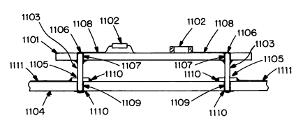
Figure 11 shows how the final assembly might look in cross-section. The
open-frame dc/dc converter has a substrate 1101 on which circuitry 1102 is
attached.
CA 02395651 2002-06-21
WO 01/47328 PCT/US00/34577
-16-
Only a few circuit components are shown in this figure for simplicity. In
general,
there would be many components mounted on both sides of the converter
substrate
1101.
Several terminal pins 1103 with flanges 1105 are swage fit into holes 1106 of
the converter substrate. These pins are then soldered to the holes in the
spaces 1107
between the pins and the side walls of the holes. Conductive traces 1108 on
the
converter substrate 1101 electrically connect the terminal pins to circuitry
1102.
The other end of pins 1103 are inserted into the printed circuit board 1104.
The shoulder of the flange 1105 of these pins abuts the printed circuit board.
Solder 1109 connects the pin 1103 and its flange 1 I OS to conductive pads on
the printed circuit board and the sidewalk of the holes. Fillets 1110 of
solder are
formed around the flanges and around the end of the pin that extends through
the
printed circuit board.
The terminal pins 1103 are connected electrically to other parts of the
printed
1 S circuit board through conductive traces 1111.
While this invention has been particularly shown and described with
references to preferred embodiments thereof, it will be understood by those
skilled
in the art that various changes in form and details may be made therein
without
departing from the scope of the invention encompassed by the appended claims.