Note: Descriptions are shown in the official language in which they were submitted.
CA 02395694 2005-08-19
WO 01/30499 PCT/US00/34999
_I_
MULTIPLE ELECTROSPRAY DEVICE, SYSTEMS AND METHODS
' '' S
FIELD OF THE INVENTION
The present invention relates genezally to an integrated miniaturized
fluidic system fabricated using Micro-ElectroMechanical System (MEMS)
technology, particularly to an integrated monolithic microfabricated device
capable of
generating multiple sprays from a single fluid stream.
BACKGROUND OF THE INVENTION
New trends in drug discovery and development are creating new
I5 demands on analytical techniques. For example, combinatorial chemistry is
often
employed to discover new lead compounds, or to create variations of a lead
compound. Combinatorial chemistry techniqfzes can generate thousands of
compounds (combinatorial libraries) in a relatively short time (on the order
of days to
weeks). Testing such a large number of compounds for biological activity in a
timely
and efficient manner zequires high-throughput screening methods which allow
rapid
evaluation of the characteristics of each candidate compound.
The quality of the combinatorial library and the compounds contained
therein is used to assess the validity of the biological screening data.
Confirmation
that the cowect molecular weight is identified for each compound or a
statistically
relevant number of compounds along with a measure of compound purity are two
important measures of the quality of a combinatorial library. Compounds can be
analytically characterized by removing a portion of solution from each well
and
injecting the con e~nts~a~separation device such as liquid chromatography or
- ' capillary electrophoresis instrument coupled to a mass spectrometer.
Development of viable screening methods for these new targets will
often depend on the availability of rapid separation and analysis techniques
for
analyzing the results of assays. Fox example, an assay for potential toxic
metabolites
of a candidate drug would need to identify both the candidate drug aad the
CA 02395694 2002-06-21
WO 01/50499 PCT/US00/34999
-2-
metabolites of that candidate. An understanding of how a new compound is
absorbed
in the body and how it is metabolized can enable prediction of the likelihood
for an
increased therapeutic effect or lack thereof.
Given the enormous number of new compounds that are being
generated daily, an improved system for identifying molecules of potential
therapeutic
value for drug discovery is also critically needed. Accordingly, there is a
critical need
for high-throughput screening and identification of compound-target reactions
in
order to identify potential drug candidates.
Liquid chromatography (LC) is a well-established analytical method
for separating components of a fluid for subsequent analysis and/or
identification.
Traditionally, liquid chromatography utilizes a separation column, such as a
cylindrical tube with dimensions 4.6 mm inner diameter by 25 cm length, filled
with
tightly packed particles of 5 ~m diameter. More recently, particles of 3 ~,m
diameter
are being used in shorter length columns. The small particle size provides a
large
surface area that can be modified with various chemistries creating a
stationary phase.
A Liquid eluent is pumped through the LC column at an optimized flow rate
based on
the column dimensions and particle size. This liquid eluent is referred to as
the
mobile phase. A volume of sample is injected into the mobile phase prior to
the LC
column. The analytes in the sample interact with the stationary phase based on
the
partition coefficients for each of the analytes. The partition coefficient is
defined as
the ratio of the time an analyte spends interacting with the stationary phase
to the time
spent interacting with the mobile phase. The longer an analyte interacts with
the
stationary phase, the higher the partition coefficient and the longer the
analyte is
retained on the LC column. The diffusion rate for an analyte through a mobile
phase
(mobile-phase mass transfer) also affects the partition coefficient. The
mobile-phase
mass transfer can be rate limiting in the performance of the separation column
when it
is greater than 2 ~,m (Knox, J.H.J. J. Chromatogr. Sci. 18:453-461 (1980)).
Increases
in chromatographic separation are achieved when using a smaller particle size
as the
stationary phase support.
The purpose of the LC column is to separate analytes such that a
unique response for each analyte from a chosen detector can be acquired for a
quantitative or qualitative measurement. The ability of a LC column to
generate a
separation is determined by the dimensions of the column and the particle size
CA 02395694 2002-06-21
WO 01/50499 PCT/US00/34999
-3-
supporting the stationary phase. A measure of the ability of LC columns to
separate a
given analyte is referred to as the theoretical plate number N. The retention
time of
an analyte can be adjusted by varying the mobile phase composition and the
partition
coefficient for an analyte. Experimentation and a fundamental understanding of
the
partition coefficient for a given analyte determine which stationary phase is
chosen.
To increase the throughput of LC analyses requires a reduction in the
dimensions of the LC column and the stationary phase particle dimensions.
Reducing
the length of the LC column from 25 cm to 5 cm will result in a factor of 5
decrease in
the retention time for an analyte. At the same time, the theoretical plates
are reduced
5-fold. To maintain the theoretical plates of a 25 cm length column packed
with 5 ~,m
particles, a 5 cm column would need to be packed with 1 p,m particles.
However, the
use of such small particles results in many technical challenges.
One of these technical challenges is the backpressure resulting from
pushing the mobile phase through each of these columns. The backpressure is a
measure of the pressure generated in a separation column due to pumping a
mobile
phase at a given flow rate through the LC column. For example, the typical
backpressure of a 4.6 mm inner diameter by 25 cm length column packed with 5
~m
particles generates a backpressure of 100 bar at a flow rate of 1.0 mL/min. A
5 cm
column packed with 1 ~,m particles generates a back pressure 5 times greater,
than a
25 cm column packed with 5 ~,m particles. Most commercially available LC pumps
are limited to operating pressures less than 400 bar and thus using an LC
column with
these small particles is not feasible.
Detection of analytes separated on an LC column has traditionally been
accomplished by use of spectroscopic detectors. Spectroscopic detectors rely
on a
change in refractive index, ultraviolet and/or visible light absorption, or
fluorescence
after excitation with a suitable wavelength to detect the separated
components.
Additionally, the effluent from an LC column may be nebulized to generate an
aerosol
which is sprayed into a chamber to measure the light scattering properties of
the
analytes eluting from the column. Alternatively, the separated components may
be
passed from the liquid chromatography column into other types of analytical
instruments for analysis. The volume from the LC column to the detector is
minimized in order to maintain the separation efficiency and analysis
sensitivity. All
CA 02395694 2002-06-21
WO 01/50499 PCT/US00/34999
-4-
system volume not directly resulting from the separation column is referred to
as the
dead volume or extra-column volume.
The miniaturization of liquid separation techniques to the nano-scale
involves small column internal diameters (< 100 ~.m i.d.) and Iow mobile phase
flow
rates (< 300 nL/min). Currently, techniques such as capillary zone
electrophoresis
(CZE), nano-LC, open tubular liquid chromatography (OTLC), and capillary
electrochromatography (CEC) offer numerous advantages over conventional scale
high performance liquid chromatography (HPLC). These advantages include higher
separation efficiencies, high-speed separations, analysis of low volume
samples; and
the coupling of 2-dimensional techniques. One challenge to using miniaturized
separation techniques is detection of the small peak volumes and a limited
number of
detectors that can accommodate these small volumes. However, coupling of low
flow
rate liquid separation techniques to electxospxay mass spectrometry results in
a
combination of techniques that are well suited as demonstrated in J.N.
Alexander IV,
et al., Rapid Commun. Mass Spectrom. 12:1187-91 (1998). The process of
electrospray at flow rates on the order of nanoliters ("nL") per minute has
been
referred to as "nanoelectrospray".
Capillary electrophoresis is a technique that utilizes the electrophoretic
nature of molecules and/or the electroosmotic flow of fluids in small
capillary tubes to
separate components of a fluid. Typically, a fused silica capillary of 100 ~,m
inner
diameter or less is filled with a buffer solution containing an electrolyte.
Each end of
the capillary is placed in a separate fluidic reservoir containing a buffer
electrolyte. A
potential voltage is placed in one of the buffer reservoirs and a second
potential
voltage is placed in the other buffer reservoir. Positively and negatively
charged
species will migrate in opposite directions through the capillary under the
influence of
the electric field established by the two potential voltages applied to the
buffer
reservoirs. Electroosmotic flow is defined as the fluid flow along the walls
of a
capillary due to the migration of charged species from the buffer solution
under the
influence of the applied electric field. Some molecules exist as charged
species when
in solution and will migrate through the capillary based on the charge-to-mass
ratio of
the molecular species. This migration is defined as electrophoretic mobility.
The
electroosmotic flow and the electrophoretic mobility of each component of a
fluid
determine the overall migration fox each fluidic component. The fluid flow
prof 1e
CA 02395694 2002-06-21
WO 01/50499 PCT/US00/34999
-5-
resulting from electroosmotic flow is flat due to the reduction in frictional
drag along
the walls of the separation channel. This results in improved separation
efficiency
compared to liquid chromatography where the flow profile is parabolic
resulting from
pressure driven flow.
Capillary electrochromatography is a hybrid technique that utilizes the
electrically driven flow characteristics of electrophoretic separation methods
within
capillary columns packed with a solid stationary phase typical of liquid
chromatography. It couples the separation power of reversed-phase liquid
chromatography with the high efficiencies of capillary electrophoresis. Higher
efficiencies are obtainable for capillary electrochromatography separations
ovex liquid
chromatography, because the flow profile resulting from electroosmotic flow is
flat
due to the reduction in frictional drag along the walls of the separation
channel when
compared to the parabolic flow profile resulting from pressure driven flows.
Furthermore, smaller particle sizes can be used in capillary
electrochromatography
than in liquid chromatography, because no backpressure is generated by
electroosmotic flow. In contrast to electrophoresis, capillary
electrochromatography
is capable of separating neutral molecules due to analyte partitioning between
the
stationary and mobile phases of the column particles using a liquid
chromatography
separation mechanism.
Microchip-based separation devices have been developed for rapid
analysis of large numbers of samples. Compared to other conventional
separation
devices, these microchip-based separation devices have higher sample
throughput,
reduced sample and reagent consumption, and reduced chemical waste. The liquid
flow rates for microchip-based separation devices range from approximately 1-
300 nanoliters per minute for most applications. Examples of microchip-based
separation devices include those for capillary electrophoresis ("CE"),
capillary
electrochromatography ("CEC") and high-performance liquid chromatography
("HPLC") include Harrison et al., Science 261:859-97 (1993); Jacobson et al.,
Anal.
Chem. 66:I 114-18 (1994), Jacobson et al., Anal. Chem. 66:2369-73 (1994),
Kutter et
al., Anal. Chem. 69:5165-71 (1997) and He et al., Anal. Chem. 70:3790-97
(1998).
Such separation devices are capable of fast analyses and provide improved
precision
and reliability compared to other conventional analytical instruments.
CA 02395694 2002-06-21
WO 01/50499 PCT/US00/34999
-6-
The work of He et al., Anal. Chem. 70:3790-97 (1998) demonstrates
some of the types of structures that can be fabricated in a glass substrate.
This work
shows that co-located monolithic support structures (or posts) can be etched
reproducibly in a glass substrate using reactive ion etching (RIE) techniques.
Currently, anisotropic RIE techniques for glass substrates axe limited to
etching
features that are 20 ~.m or less in depth. This work shows rectangular 5 ~m by
5 ~m
width by 10 ~,m in depth posts and stated that deeper structures were
difficult to
achieve. The posts are also separated by 1.5 ~,m. The posts supports the
stationary
phase just as with the particles in LC and CEC columns. An advantage to the
posts
over conventional LC and CEC is that the stationary phase support structures
are
monolithic with the substrate and therefore, immobile.
He et, al., also describes the importance of maintaining a constant
cross-sectional area across the entire length of the separation channel. Large
variations in the cross-sectional area can create pressure drops in pressure
driven flow
systems. In electrokinetically driven flow systems, large variations in the
cross-
sectional area along the length of a separation channel can create flow
restrictions that
result in bubble formation in the separation channel. Since the fluid flowing
through
the separation channel functions as the source and carrier of the mobile
solvated ions,
formation of a bubble in a separation channel will result in the disruption of
the
electroosmotic flow.
Electrospray ionization provides for the atmospheric pressure
ionization of a liquid sample. The electrospray process creates highly-charged
droplets that, under evaporation, create ions representative of the species
contained in
the solution. An ion-sampling orifice of a mass spectrometer may be used to
sample
these gas phase ions for mass analysis. When a positive voltage is applied to
the tip
of the capillary relative to an extracting electrode, such as one provided at
the ion-
sampling orifice of a mass spectrometer, the electric field causes positively-
charged
ions in the fluid to migrate to the surface of the fluid at the tip of the
capillary. When
a negative voltage is applied to the tip of the capillary relative to an
extracting
electrode, such as one provided at the ion-sampling orifice to the mass
spectrometer,
the electric field causes negatively-charged ions in the fluid to migrate to
the surface
of the fluid at the tip of the capillary.
CA 02395694 2002-06-21
WO 01/50499 PCT/US00/34999
7_
When the repulsion force of the solvated ions exceeds the surface
tension of the fluid being electrosprayed, a volume of the fluid is pulled
into the shape
of a cone, known as a Taylor cone, which extends from the tip of the
capillary. A
liquid jet extends from the tip of the Taylor cone and becomes unstable and
generates
charged-droplets. These small charged droplets are drawn toward the extracting
electrode. The small droplets are highly-charged and solvent evaporation from
the
droplets results in the excess charge in the droplet residing on the analyte
molecules in
the electrosprayed fluid. The charged molecules or ions are drawn through the
ion-
sampling orifice of the mass spectrometer for mass analysis. This phenomenon
has
been described, for example, by Dole et al., Chem. Phys. 49:2240 (1968) and
Yamashita et al., J. Phys. Chem. 88:4451 (1984). The potential voltage ("V")
required to initiate an electrospray is dependent on the surface tension of
the solution
as described by, for example, Smith, IEEE Trans. Ind. Appl. 1986, IA-22:527-35
(1986). Typically, the electric field is on the order of approximately 106
V/m. The
1 S physical size of the capillary and the fluid surface tension determines
the density of
electric field lines necessary to initiate electrospray.
When the repulsion force of the solvated ions is not sufficient to
overcome the surface tension of the fluid exiting the tip of the capillary,
large poorly
charged droplets are formed. Fluid droplets are produced when the
electrical.potential
difference applied between a conductive or partly conductive fluid exiting a
capillary
and an electrode is not sufficient to overcome the fluid surface tension to
form a
Taylor cone.
Electrospray Ionization Mass Spectrometry: Fundamentals,
Instrumentation, and At~plications, edited by R.B. Cole, ISBN 0-471-14564-5,
John
Wiley & Sons, Inc., New York summarizes much of the fundamental studies of
electrospray. Several mathematical models have been generated to explain the
principals governing electrospray. Equation 1 defines the electric field E~ at
the tip of
a capillary of radius r~ with an applied voltage V~ at a distance d from a
counter
electrode held at ground potential:
_ 2V~ ( )
E~ r~.~n(4d l r~) 1
CA 02395694 2002-06-21
WO 01/50499 PCT/US00/34999
_g-
The electric field E°" required for the formation of a Taylor cone
and
liquid jet of a fluid flowing to the tip of this capillary is approximated as:
1/2
E _ 2y cos0 (2)
OJJ N
EO~C
where y is the surface tension of the fluid, 8 is the half angle of the
Taylor cone and so is the permittivity of vacuum. Equation 3 is derived by
combining
equations 1 and 2 and approximates the onset voltage V°" required to
initiate an
electrospray of a fluid from a capillary:
nz
~°Y cos9 ~y~(4d l r~) (3)
2s°
As can be seen by examination of equation 3, the required onset
voltage is more dependent on the capillary radius than the distance from the
counter-
electrode.
It would be desirable to define an electrospray device that could form a
stable electrospray of all fluids commonly used in CE, CEC, and LC. The
surface
tension of solvents commonly used as the mobile phase for these separations
range
from 100% aqueous (y = 0.073 N/m) to 100% methanol (y = 0.0226 N/m). As the
surface tension of the electrospray fluid increases, a higher onset voltage is
required to
initiate an electrospray for a fixed capillary diameter. As an example, a
capillary with
a tip diameter of 14 ~,m is required to electrospray 100% aqueous solutions
with an
onset voltage of 1000 V. The work of M.S. Wilm et al., Int. J. Mass Spectrom.
Ion
Processes 136:167-80 (1994), first demonstrates nanoelectrospray from a fused-
silica
capillary pulled to an outer diameter of 5 ~m at a flow rate of 25 nL/min.
Specifically, a nanoelectrospray at 25 nL/min was achieved from a 2 ~m inner
diameter and 5 ~,m outer diameter pulled fused-silica capillary with 600-700 V
at a
distance of 1-2 mm from the ion-sampling orifice of an electrospray equipped
mass
spectrometer.
CA 02395694 2002-06-21
WO 01/50499 PCT/US00/34999
-9-
Electrospray in front of an ion-sampling orifice of an API mass
spectrometer produces a quantitative response from the mass spectrometer
detector
due to the analyte molecules present in the liquid flowing from the capillary.
One
advantage of electrospray is that the response for an analyte measured by the
mass
spectrometer detector is dependent on the concentration of the analyte in the
fluid and
independent of the fluid flow rate. The response of an analyte in solution at
a given
concentration would be comparable using electrospray combined with mass
spectrometry at a flow rate of 100 ~L/min compared to a flow rate of 100
nL/min.
D.C. Gale et al., Rapid Commun. Mass Spectrom. 7:1017 (1993) demonstrate that
higher electrospray sensitivity is achieved at lower flow rates due to
increased analyte
ionization efficiency. Thus by performing electrospray on a fluid at flow
rates in the
nanoliter per minute range provides the best sensitivity for an analyte
contained
within the fluid when combined with mass spectrometry.
Thus, it is desirable to provide an electrospray device for integration of
microchip-based separation devices with API-MS instruments. This integration
places a restriction on the capillary tip defining a nozzle on a microchip.
This nozzle
will, in all embodiments, exist in a planar or near planar geometry with
respect to the
substrate defining the separation device and/or the electrospray device. When
this co-
planar or near planar geometry exists, the electric field lines emanating from
the tip of
the nozzle will not be enhanced if the electric field around the nozzle is not
defined
and controlled and, therefore, an electrospray is only achievable with the
application
of relatively high voltages applied to the fluid.
Attempts have been made to manufacture an electrospray device for
microchip-based separations. Ramsey et al., Anal. Chem. 69:1174-78 (1997)
describes a microchip-based separations device coupled with an electrospray
mass
spectrometer. Previous work from this research group including Jacobson et
al., Anal.
Chem. 66:1114-18 (1994) and Jacobson et al., Anal. Chem. 66:2369-73 (1994)
demonstrate impressive separations using on-chip fluorescence detection. This
more
recent work demonstrates nanoelectrospray at 90 nL/min from the edge of a
planar
glass microchip. The microchip-based separation cl?annel has dimensions of 10
~m
deep, 60 ~,m wide, and 33 mm in length. Electroosmotic flow is used to
generate
fluid flow at 90 nL/min. Application of 4,800 V to the fluid exiting the
separation
CA 02395694 2002-06-21
WO 01/50499 PCT/US00/34999
-10-
channel on the edge of the microchip at a distance of 3-5 mm from the ion-
sampling
orifice of an API mass spectrometer generates an electrospray. Approximately
12 nL
of the sample fluid collects at the edge of the microchip before the formation
of a
Taylor cone and stable nanoelectrospray from the edge of the, microchip. The
volume
of this microchip-based separation channel is 19.8 nL. Nanoelectrospray from
the
edge of this microchip device after capillary electrophoresis or capillary
electrochromatography separation is rendered impractical since this system has
a
dead-volume approaching 60% of the column (channel) volume. Furthermore,
because this device provides a flat surface, and, thus, a relatively small
amount of
physical asperity for the formation of the electrospray, the device requires
an
impractically high voltage to overcome the fluid surface tension to initiate
an
electrospray.
Xue,,Q. et al., Anal. Chem. 69:426-30 (1997) also describes a stable
nanoelectrospray from the edge of a planar glass microchip with a closed
channel
25 ~m deep, 60 ~m wide, and 35-50 mm in length. An electrospray is formed by
applying 4,200 V to the fluid exiting the separation channel on the edge of
the
microchip at a distance of 3-8 mm from the ion-sampling orifice of an API mass
spectrometer. A syringe pump is utilized to deliver the sample fluid to the
glass
microchip at a flow rate of 100 to 200 nL/min. The edge of the glass microchip
is
treated with a hydrophobic coating to alleviate some of the difficulties
associated with
nanoelectrospray from a flat surface that slightly improves the stability of
the
nanoelectrospray. Nevertheless, the volume of the Taylor cone on the edge of
the
microchip is too large relative to the volume of the separation channel,
making this
method of electrospray directly from the edge of a microchip impracticable
when
combined with a chromatographic separation device.
T. D. Lee et. al., 1997 International Conference on Solid-State Sensors
and Actuators Chicago, pp. 927-30 (June 16-19, 1997) describes a mufti-step
process
to generate a nozzle on the edge of a silicon microchip 1-3 ~,m in diameter or
width
and 40 ~.m in length and applying 4,000 V to the entire microchip at a
distance of
0.25-0.4 mm from the ion-sampling orifice of an API mass spectrometer. Because
a
relatively high voltage is required to form an electrospray with the nozzle
positioned
in very close proximity to the mass spectrometer ion-sampling orifice, this
device
CA 02395694 2002-06-21
WO 01/50499 PCT/US00/34999
-11-
produces an inefficient electrospray that does not allow for sufficient
droplet
evaporation before the ions enter the orifice. The extension of the nozzle
from the
edge of the microchip also exposes the nozzle to accidental breakage. More
recently,
T. D. Lee et.al., in 1999 Twelfth IEEE International Micro Electro Mechanical
Systems Conference (January 17-21, 1999), presented this same concept where
the
electrospray component was fabricated to extend 2.5 mm beyond the edge of the
microchip to overcome this phenomenon of poor electric field control within
the
proximity of a surface.
Thus, it is also desirable to provide an electrospray device with
controllable spraying and a method for producing such a device that is easily
reproducible and manufacturable in high volumes.
U.S. Patent 5,501,93 to Laermer et. al., reports a method of
anisotropic plasma etching of silicon (Bosch process) that provides a method
of
producing deep vertical structures that is easily reproducible and
controllable. This
method of anisotropic plasma etching of silicon incorporates a two step
process. Step
one is an anisotropic etch step using a reactive ion etching (RTE) gas plasma
of sulfur
hexafluoride (SF6). Step two is a passivation step that deposits a polymer on
the
vertical surfaces of the silicon substrate. This polymerizing step provides an
etch stop
on the vertical surface that was exposed in step one. This two step cycle of
etch and
passivation is repeated until the depth of the desired structure is achieved.
This
method of anisotropic plasma etching provides etch rates over 3 ~m/min of
silicon
depending on the size of the feature being etched. The process also provides
selectivity to etching silicon versus silicon dioxide or resist of greater
than 100:1
which is important when deep silicon structures are desired. Laermer et. al.,
in 1999
Twelfth IEEE International Micro Electro Mechanical Systems Conference
(January
17-21, 1999), reported improvements to the Bosch process. These improvements
include silicon etch rates approaching 10 ~,m/min, selectivity exceeding 300:1
to
silicon dioxide masks, and more uniform etch rates for features that vary in
size.
The present invention is directed toward a novel utilization of these
features to improve the sensitivity of prior disclosed microchip-based
electrospray
systems.
CA 02395694 2002-06-21
WO 01/50499 PCT/US00/34999
-12-
SUMMARY OF THE INVENTION
The present invention relates to an electrospray device for spraying a
fluid which includes an insulating substrate having an injection surface and
an
ejection surface opposing the injection surface. The substrate is an integral
monolith
having either a single spray unit or a plurality of spray units for generating
multiple
sprays from a single fluid stream. Each spray unit includes an entrance
orifice on the
injection surface; an exit orifice on the ejection surface; a channel
extending between
the entrance orifice and the exit orifice; and a recess surrounding the exit
orifice and
positioned between the injection surface and the ejection surface. The
entrance
orifices for each of the plurality of spray units are in fluid communication
with one
another and each spray unit generates an electrospray plume of the fluid. The
electrospray device also includes an electric field generating source
positioned to
define an electric field surrounding the exit oxifice. In one embodiment, the
electric
field generating source includes a first electrode attached to the substrate
to impart a
first potential to the substrate and a second electrode to impart a second
potential.
The first and the second electrodes are positioned to defne an electric field
surrounding the exit orifice. This device can be operated to generate multiple
electxospray plumes of fluid from each spray unit, to generate a single
combined
electxospray plume of fluid from a plurality of spray units, and to generate
multiple
electrospray plumes of fluid from a plurality of spray units. The device can
also be
used in conjunction with a system for processing an electrospray of fluid, a
method of
generating an electrospray of fluid, a method of mass spectrometric analysis,
and a
method of liquid chxomatographic analysis.
Another aspect of the present invention is directed to an electrospray
system for generating multiple sprays from a single fluid stream. The system
includes
an array of a plurality of the above electrospray devices. The electrospray
devices
can be provided in the array at a device density exceeding about 5
devices/cm2, about
16 devices/cm2, about 30 devices/crn~, or about 81 devices/cm2. The
electrospray
devices can also be provided in the array at a device density of from about 30
devices/cm2 to about 100 devices/cm2.
Another aspect of the present invention is directed to an array of a
plurality of the above electrospray devices for generating multiple sprays
fxom a
single fluid stream. The electrospray devices can be provided in an array
wherein the
CA 02395694 2002-06-21
WO 01/50499 PCT/US00/34999
-13-
spacing on the ejection surface between adjacent devices is about 9 mm or
less, about
4.5 mm or less, about 2.2 mm or less, about 1.1 mm or less, about 0.56 mm or
less, or
about 0.28 mm or less, respectively.
Another aspect of the present invention is directed to a method of
generating an electrospray wherein an electrospray device is provided for
spraying a
fluid. The electospray device includes a substrate having an injection surface
and an
ejection surface opposing the injection surface. The substrate is an integral
monolith
which includes an entrance orifice on the injection surface; an exit orifice
on the
ejection surface; a channel extending between the entrance orifice and the
exit orifice;
~ and a recess surrounding the exit orifice and positioned between the
injection surface
and the ejection surface. The method can be performed to generate multiple
electrospray.plumes of fluid from each spray unit, to generate a single
combined
electrospray plume of fluid from a plurality of spray units, and to generate
multiple
electrospray plumes of fluid from a plurality of spray units. The electrospray
device
also includes an electric field generating source positioned to define an
electric field
surrounding the exit orifice. In one embodiment, the electric field generating
source
includes a first electrode attached to the substrate to impart a first
potential to the
substrate and a second electrode to impart a second potential. The first and
the second
electrodes are positioned to define an electric field surrounding the exit
orifice.
Analyte from a fluid sample is deposited on the injection surface and then
eluted with
an eluting fluid. The eluting fluid containing analyte is passed into the
entrance
orifice through the channel and through the exit orifice. A first potential is
applied to
the first electrode and a second potential is applied to the fluid through the
second
electrode. The first and second potentials are selected such that fluid
discharged from
the exit orifice of each of the spray units forms an electrospray.
Another aspect of the present invention is directed to a method of
producing an electrospray device which includes providing a substrate having
opposed first and second surfaces, each coated with a photoresist over an etch-
resistant material. The photoresist on the first surface is exposed to an
image to form a
pattern in the form of at least one ring on the first surface. The photoresist
on the first
surface which is outside and inside the at least one ring is then removed to
form an
annular portion. The etch-resistant material is removed from the first surface
of the
substrate where the photoresist is removed to form holes in the etch-resistant
material.
CA 02395694 2002-06-21
WO 01/50499 PCT/US00/34999
-14-
Photoresist remaining on the first surface is then optionally removed. The
first surface
is then coated with a second coating of photoresist. The second coating of
photoresist
within the at least one ring is exposed to an image and removed to form at
least one
hole. The material from the substrate coincident with the at least one hole
in.the
second layer of photoresist on the first surface is removed to form at least
one passage
extending through the second layer of photoresist on the first surface and
into the
substrate. Photoresist from the first surface is then removed. An etch-
resistant layer
is applied to all exposed surfaces on,the first surface side of the substrate.
The etch-
resistant layer from the first surface that is around the at least one ring
and the
material from the substrate around the at least one ring axe removed to define
at least
one nozzle on the first surface. The photoresist on the second surface is then
exposed
to an image to form a pattern circumscribing extensions of the at least one
hole
formed in the etch-resistant material of the first surface. The etch-resistant
material
on the second surface is then removed where the pattern is. Material is
removed from
the substrate coincident with where the pattern in the photoresist on the
second
surface has been removed to form a reservoir extending into the substrate to
the extent
needed to join the reservoir and the at least one passage. An etch-resistant
material is
then applied to all exposed surfaces of the substrate to form the electrospray
device.
The method further includes the step of applying a silicon nitride layer over
all
surfaces after the etch-resistant material is applied to all exposed surfaces
of the
substrate.
Another aspect of the present invention is directed another method of
producing an electrospray device including providing a substrate having
opposed first
and second surfaces, the first side coated with a photoresist over an etch-
resistant .
material. The photoresist on the first surface is exposed to an image to form
a pattern
in the form of at least one ring on the first surface. The exposed photoresist
is
removed on the first surface which is outside and inside the at least one ring
leaving
the unexposed photoresist. The etch-resistant material is removed from the
first
surface of the substrate where the exposed photoresist was removed to form
holes in
the etch-resistant material. Photoresist is removed from the first surface.
Photoresist
is provided over an etch-resistant material on the second surface and exposed
to an
image to form a pattern circumscribing extensions of the at least one ring
formed in
the etch-resistant material of the first surface. The exposed photoresist on
the second
CA 02395694 2002-06-21
WO 01/50499 PCT/US00/34999
-15-
surface is removed. The etch-resistant material on the second surface is
removed
coincident with where the photoresist was removed. Material is removed from
the
substrate coincident with where the etch-resistant material on the second
surface was
removed to form a reservoir extending into the substrate. The remaining
photoresist
on the second surface is removed. The second surface is coated with an etch-
resistant
material. The first surface is coated with a second coating of photoresist.
The second
coating of photoresist within the at least one ring is exposed to an image.
The
exposed second coating of photoresist is removed from within the at least one
ring to
form at least one hole. Material is removed from the substrate coincident with
the at
least one hole in the second layer of photoresist on the first surface to form
at least
one passage extending through the second layer of photoresist on the first
surface and
into substrate to the extent needed to reach the etch-resistant material
coating the
reservoir. Photoresist from the first surface is removed. Material is removed
from the
substrate exposed by the removed etch-resistant layer around the at least one
ring to
I S define at least one nozzle on the first surface. The etch-resistant
material coating the
reservoir is removed from the substrate. An etch resistant material is applied
to coat
all exposed surfaces of the substrate to form the electrospray device.
The electrospray device of the present invention can generate multiple
electrospray plumes from a single fluid stream and be simultaneously combined
with
mass spectrometry. Each electrospray plume generates a signal for an analyte
contained within a fluid that is proportional to that analytes concentration.
When
multiple electrospray plumes are generated from one nozzle, the ion intensity
for a
given analyte will increase with the number of electrospray plumes emanating
from
that nozzle as measured by the mass spectrometer. When multiple nozzle arrays
generate one or more electrospray plumes, the ion intensity will increase with
the
number of nozzles times the number of electrospray plumes emanating from the
nozzle arrays.
The present invention achieves a significant advantage in terms of
high-sensitivity analysis of analytes by electrospray mass spectrometry. A
method of
control of the electric field around closely positioned electrospray nozzles
provides a
method of generating multiple electrospray plumes from closely positioned
nozzles in
a well-controlled process. An array of electrospray nozzles is disclosed
for~generation
of multiple electrospray plumes of a solution for purpose of generating an ion
CA 02395694 2002-06-21
WO 01/50499 PCT/US00/34999
-16-
response as measured by a mass spectrometer that increases with the total
number of
generated electrospray plumes. The present invention achieves a significant
advantage in comparison to prior disclosed electrospray systems and methods
for
combination with microfluidic chip-based devices incorporating a single nozzle
forming a single electrospray.
The electrospray device of the present invention generally includes a
silicon substrate material defining a channel between an entrance orifice on
an
injection surface and a nozzle on an ejection surface (the major surface) such
that the
electrospray generated by the device is generally perpendicular to the
ejection surface.
The nozzle has an inner and an outer diameter and is defined by an annular
portion
recessed from the ejection surface. The recessed annular region extends
radially from
the outer diameter. The tip of the nozzle is co-planar or level with and does
not
extend beyond the ejection surface. Thus, the nozzle is protected against
accidental
breakage. The nozzle, the channel, and the recessed annular region are etched
from
the silicon substrate by deep reactive-ion etching and other standard
semiconductor
processing techniques.
All surfaces of the silicon substrate preferably have insulating layers
thereon to electrically isolate the liquid sample from the substrate and the
ejection and
injection surfaces from each other such that different potential voltages may
be
individually applied to each surface, the silicon substrate and the liquid
sample. The
insulating layer generally constitutes a silicon dioxide layer combined with a
silicon
nitride layer. The silicon nitride layer provides a moisture barrier against
water and
ions from penetrating through to the substrate thus preventing electrical
breakdown
between a fluid moving in the channel and the substrate. The electrospray
apparatus
preferably includes at least one controlling electrode electrically contacting
the
substrate for the application of an electric potential to the substrate.
Preferably, the nozzle, channel and recess are etched from the silicon
substrate by reactive-ion etching and other standard semiconductor processing
techniques. The injection-side features, through-substrate fluid channel,
ejection-side
features, and controlling electrodes are formed monolithically from a
monocrystalline
silicon substrate -- i.e., they are formed during the course of and as a
result of a
fabrication sequence that requires no manipulation or assembly of separate
components.
CA 02395694 2002-06-21
WO 01/50499 PCT/US00/34999
Because the electrospray device is manufactured using reactive-ion
etching and other standard semiconductor processing techniques, the dimensions
of
such a device nozzle can be very small, for example, as small as 2 ~,m inner
diameter
and 5 ~,m outer diameter. Thus, a through-substrate fluid channel having, for
example, 5 ~,m inner diameter and a substrate thickness of 250 ~,m only has a
volume
of 4.9 pL ("picoliters"). The micrometer-scale dimensions of the electrospray
device
minimize the dead volume and thereby increase efficiency and analysis
sensitivity
when combined with a separation device.
The electrospray device of the present invention provides for the
efficient and effective formation of an electrospray. By providing an
electrospray
surface (i.e., the tip of the nozzle) from which the fluid is ejected with
dimensions on
the order of micrometers, the device limits the voltage required to generate a
Taylor
cone and subsequent electrospray. The nozzle of the electrospray device
provides the
physical asperity on the order of micrometers on which a large electric field
is
concentrated. Further, the nozzle of the electrospray device contains a thin
region of
conductive silicon insulated from a fluid moving through the nozzle by the
insulating
silicon dioxide and silicon nitride layers. The fluid and substrate voltages
and the
thickness of the insulating layers separating the silicon substrate from the
fluid
determine the electric field at the tip of the nozzle. Additional electrodes)
on the
ejection surface to which electric potentials) may be applied and controlled
independent of the electric potentials of the fluid and the substrate may be
incorporated in order to advantageously modify and optimize the electric field
in
order to focus the gas phase ions produced by the electrospray.
The microchip-based electrospray device of the present invention
provides minimal extra-column dispersion as a result of a reduction in the
extra-
column volume and provides efficient, reproducible, reliable and rugged
formation of
an electrospray. This electrospray device is perfectly suited as a means of
electrospray of fluids from microchip-based separation devices. The design of
this
electrospray device is also robust such that the device can be readily mass-
produced
in a cost-effective, high-yielding process.
The electrospray device may be interfaced to or integrated downstream
from a sampling device, depending on the particular application. For example,
the
CA 02395694 2002-06-21
WO 01/50499 PCT/US00/34999
-18-
analyte may be electrosprayed onto a surface to coat that surface or into
another
device for purposes of conveyance, analysis, and/or synthesis. As described
previously, highly charged droplets are formed at atmospheric pressure by the
electrospray device from nanoliter-scale volumes of an analyte. The highly
charged
droplets produce gas-phase ions upon sufficient evaporation of solvent
molecules
which may be sampled, for example, through an ion-sampling orifice of an
atmospheric pressure ionization mass spectrometer ("API-MS") for analysis of
the
electrosprayed fluid.
A multi-system chip thus provides a rapid sequential chemical analysis
system fabricated using Micro-ElectroMechanical System ("MEMS") technology.
The mufti-system chip enables automated, sequential separation and injection
of a
multiplicity of samples, resulting in significantly greater analysis
throughput and
utilization of the mass spectrometer instrument for high-throughput detection
of
compounds for drug discovery.
Another aspect of the present invention provides a silicon microchip-
based electrospray device for producing electrospray of a liquid sample. The
electrospray device may be interfaced downstream to an atmospheric pressure
ionization mass spectrometer ("API-MS") for analysis of the electrosprayed
fluid.
The use of multiple nozzles for electrospray of fluid from the same
fluid stream extends the useful flow rate range of microchip-based
electrospray
devices. Thus, fluids may be introduced to the multiple electrospray device at
higher
flow rates as the total fluid flow is split between all of the nozzles. For
example, by
using 10 nozzles per fluid channel, the total flow can be 10 times higher than
when
using only one nozzle per fluid channel. Likewise, by using 100 nozzles per
fluid
channel, the total flow can be 100 times higher than when using only one
nozzle per
fluid channel. The fabrication methods used to form these electrospray nozzles
allow
for multiple nozzles to be easily combined with a single fluid stream channel
greatly
extending the useful fluid flow rate range and increasing the mass spectral
sensitivity
for microfluidic devices.
CA 02395694 2002-06-21
WO 01/50499 PCT/US00/34999
-19-
BRIEF DESCRIPTION OF THE DRAWINGS
Figure 1A shows a plan view of a one-nozzle electrospray device of
the present invention.
Figure I B shows a plan view of a two-nozzle electrospray device of
the present invention.
Figure 1 C shows a plan view of a three-nozzle electrospray device of
the present invention.
Figure 1D shows a plan view of a fourteen-nozzle electrospray device
of the present invention.
Figure 2A shows a perspective view of a one-nozzle electrospray
device of the present invention.
Figure 2B shows a perspective view of a two-nozzle electrospray
device of the present invention.
I S Figure 2C shows a perspective view of a three-nozzle electrospray
device of the present invention.
Figure 2D shows a perspective view of a fourteen-nozzle electrospray
device of the present invention.
Figure 3A shows a cross-sectional view of a one-nozzle electrospray
device of the present invention.
Figure 3B shows a cross-sectional view of a two-nozzle electrospray
device of the present invention.
Figure 3C shows a cross-sectional view of a three-nozzle electrospxay
device of the present invention.
Figure 3D shows a cross-sectional view of a fourteen-nozzle
electrospray device of the present invention.
Figure 4 is a perspective view of the injection or reservoir side of an
electrospray device of the present invention.
Figure SA shows a cross-sectional view of a two-nozzle electrospray
device of the present invention generating one electrospray plume from each
nozzle.
Figure SB shows a cross-sectional view of a two-nozzle electrospray
device of the present invention generating two electrospray plumes from each
nozzle.
CA 02395694 2002-06-21
WO 01/50499 PCT/US00/34999
-20-
Figure 6A shows a perspective view of a one-nozzle electrospray
device of the present invention generating one electrospray plume from one
nozzle.
Figure 6B shows a perspective view of a one-nozzle electrospray
device of the present invention generating two electrospray plumes from one
nozzle.
Figure 6C shows a perspective view of a one-nozzle electrospray
device of the present invention generating three electrospray plumes from one
nozzle.
Figure 6D shows a perspective view of a one-nozzle electrospray
device of the present invention generating four electrospray plumes from one
nozzle.
Figure 7A shows a video capture picture of a microfabricated
electrospray nozzle generating one electrospray plume from one nozzle.
Figure 7B shows a video capture picture of a microfabricated
electrospray nozzle generating two electrospray plumes from one nozzle.
Figure 8A shows the total ion chromatogram ("TIC") of a solution
undergoing electrospray.
Figure 8B shows the mass chromatogram for the protonated analyte at
m/z 315. Region 1 is the resulting ion intensity from one electrospray plume
from
one nozzle. Region 2 is from two electrospray plumes from one nozzle. Region 3
is
from three electrospray plumes from one nozzle. Region 4 is from four
electrospray
plumes from one nozzle. Region 5 is from two electrospray plumes from one
nozzle.
Figure 9A shows the mass spectrum from Region 1 of Figure 8B.
Figure 9B shows the mass spectrum from Region 2 of Figure 8B.
Figure 9C shows the mass spectrum from Region 3 of Figure 8B.
Figure 9D shows the mass spectrum from Region 4 of Figure 8B.
Figure 10 is a chart of the ion intensity for m/z 315 versus the number
of electrospray plumes emanating from one nozzle.
Figure 1 1A is a plan view of a two by two array of groups of four
nozzles of an electrospray device.
Figure 11B is a perspective view of a two by two array of groups of
four nozzles taken through a line through one row of nozzles.
Figure 11 C is a cross-sectional view of a two by two array of groups of
four nozzles of an electrospray device.
Figure 12A is a cross-sectional view of a 20 ~m diameter nozzle with
a nozzle height of 50 Vim. The fluid has a voltage of 1000V, substrate has a
voltage of
CA 02395694 2002-06-21
WO 01/50499 PCT/US00/34999
-21 -
zero V and a third electrode (not shown due to the scale of the figure) is
located S mm
from the substrate and has a voltage of zero V. The equipotential field Lines
are
shown in increments of SO V. .
Figure 12B is an expanded region around the nozzle shown in Figure
S 12A.
Figure 12C is a cross-sectional view of a 20 ~,m diameter nozzle with
a nozzle height of 50 ~,m. The fluid has a voltage of 1000V, substrate has a
voltage of
zero V and a third electrode (not shown due to the scale of the figure) is
located S mm
from the substrate and has a voltage of 800 V. The equipotential field lines
are shown
in increments of SO V.
Figure 12D is a cross-sectional view of a 20 p,m diameter nozzle with
a nozzle height of SO ~,m. The fluid has a voltage of 1000V, substrate has a
voltage of
800 V and a third electrode (not shown due to the scale of the figure) is
located S mm
from the substrate and has a voltage of zero V. The equipotential field lines
are
shown in increments of SO V.
Figures 13A-13C are cross-sectional views of an electrospray device
of the present invention illustrating the transfer of a discreet sample
quantity to a
reservoir contained on the substrate surface.
Figure 13D is a cross-sectional view of an electrospray device of the
present invention illustrating the evaporation of the solution leaving an
analyte
contained within the fluid on the surface of the reservoir.
Figure 13E is a cross-sectional view of an electrospray device of the
present invention illustrating a fluidic probe sealed against the injection
surface
delivering a reconstitution fluid to redissolve the analyte for electrospray
mass
2S spectrometry analysis.
Figure 14A is a plan view of mask one of an electrospray device.
Figure 14B is a cross-sectional view of a silicon substrate 200 showing
silicon dioxide layers 210 and 212 and photoresist layer 208.
Figure 14C is a cross-sectional view of a silicon substrate 200 showing
removal of photoresist layer 208 to form a pattern of 204 and 206 in the
photoresist.
CA 02395694 2002-06-21
WO 01/50499 PCT/US00/34999
-22-
Figure 14D is a cross-sectional view of a silicon substrate 200 showing
xemoval of silicon dioxide 210 from the regions 212 and 214 to expose the
silicon
substrate in these regions to form a pattern of 204 and 206 in the silicon
dioxide 210.
Figure 14E is a cross-sectional view of a silicon substrate 200 showing
removal of photoresist 208.
Figure 1 SA is a plan view of mask two of an electrospray device.
Figure 1 SB is a cross-sectional view of a silicon substrate 200 of
Figure 14E with a new layer of photoresist 208'.
Figure 15C is a cross-sectional view of a silicon substrate 200 showing
of removal of photoresist layer 208' to form a pattern of 204 in the
photoresist and
exposing the silicon substrate 218.
Figure 15D is a cross-sectional view of a silicon substrate 200 showing
the removal of silicon substrate material from the region 218 to form a
cylinder 224.
Figure 15E is a cross-sectional view of a silicon substrate 200 showing
removal of photoresist 208'.
Figure 15F is a cross-sectional view of a silicon substrate 200 showing
thermal oxidation of the exposed silicon substrate 200 to form a layer of
silicon
dioxide 226 and 228 on exposed silicon horizontal and vertical surfaces,
respectively.
Figure ISG is a cross-sectional view of a silicon substrate 200 showing
selective removal of silicon dioxide 226 from all horizontal surfaces.
Figure 15H is a cross-sectional view of a silicon substrate 200 showing
removal of silicon substrate 220 to form an annular space 230 around the
nozzles 232
Figure 16A is a plan view of mask three of an electrospray device
showing reservoir 234.
Figure 16B is a cross-sectional view of a silicon substrate 200 of
Figure 15I with a new layer of photoresist 232 on silicon dioxide 212.
Figure 16C is a cross-sectional view of a silicon substrate 200 showing
removal of photoresist layer 232 to form a pattern 234 in the photoresist
exposing
silicon dioxide 236.
Figure 16D is a cross-sectional view of a silicon substrate 200 showing
removal of silicon dioxide 236 from region 234 to expose silicon 238 in the
pattern of
234.
CA 02395694 2002-06-21
WO 01/50499 PCT/US00/34999
- 23 -
Figure 16E is a cross-sectional view of a silicon substrate 200 showing
removal of silicon 238 from region 234 to form reservoir 240 in the pattern of
234.
Figure 16F is a cross-sectional view of a silicon substrate 200 showing
removal of photoresist 232.
Figure 16G is a cross-sectional view of a silicon substrate 200 showing
thermal oxidation of the exposed silicon substrate 200 to form a layer of
silicon
dioxide 242 on all exposed silicon surfaces.
Figure 16H is a cross-sectional view of a silicon substrate 200 showing
low pressure vapor deposition of silicon nitride 244 conformally coating all
surfaces
of the electrospray device 300.
Figure 16I is a cross-sectional view of a silicon substrate 200 showing
metal deposition of electrode 246 on silicon substrate 200.
Figure 17A is a plan view of mask four of an electrospray device.
Figure 17B is a cross-sectional view of a silicon substrate 300 showing
silicon dioxide layers 310 and 312 and photoresist layer 308.
Figure 17C is a cross-sectional view of a silicon substrate 300 showing
removal of photoresist layer 308 to form a pattern of 304 and 306 in the
photoresist.
Figure 17D is a cross-sectional view of a silicon substrate 300 showing
removal of silicon dioxide 310 from the regions 318 and 320 to expose the
silicon
substrate in these regions to form a pattern of 204 and 206 in the silicon
dioxide 310.
Figure 17E is a cross-sectional view of a silicon substrate 300 showing
removal of photoresist 308.
Figure 18A is a plan view of mask five of an electrospray device.
Figure I8B is a cross-sectional view of a silicon substrate 300 showing
deposition of a film of positive-working photoresist 326 on the silicon
dioxide layer
312.
Figure 18C is a cross-sectional view of a silicon substrate 300 showing
removal of exposed areas 324 of photoresist layer 326.
Figure 18D is a cross-sectional view of a silicon substrate 300 showing
etching of the exposed area 328 of the silicon dioxide layer 312.
Figure 18E is a cross-sectional view of a silicon substrate 300 showing
the etching of reservoir 332.
CA 02395694 2002-06-21
WO 01/50499 PCT/US00/34999
-24-
Figure 18F is a cross-sectional view of a silicon substrate 300 showing
removal of the remaining photoresist 326.
Figure 18G is a cross-sectional view of a silicon substrate 300 showing
deposition of the silicon dioxide layer 334.
S Figure 19A is a plan view of mask six of an electrospray device
showing through-wafer channels 304.
Figure 19B is a cross-sectional view of a silicon substrate 300 showing
deposition of a layer of photoresist 308' on silicon dioxide layer 310.
Figure 19C is a cross-sectional view of a silicon substrate 300 showing
removal of the exposed area 304 of the photoresist.
Figure 19D is a cross-sectional view of a silicon substrate 300 showing
etching of the through-wafer channels 336.
Figure 19E is a cross-sectional view of a silicon substrate 300 showing
removal of photoresist 308'.
Figure 19F is a cross-sectional view of a silicon substrate 300 showing
removal of silicon substrate 320 to form an annular space 338 around the
nozzles.
Figure 19G is a cross-sectional view of a silicon substrate 300 showing
removal of silicon dioxide layers 310, 312 and 334.
Figure 20A is a cross-sectional view of a silicon substrate 300 showing
deposition of silicon dioxide layer 342 coating all silicon surfaces of the
electrospray
device 300.
Figure 20B is a cross-sectional view of a silicon substrate 300 showing
deposition of silicon nitride layer 344 coating all surfaces of the
electrospray device
300.
2S Figure 20C is a cross-sectional view of a silicon substrate 300 showing
metal deposition of electrodes 346 and 348.
Figures 21A and 21B show a perspective view of scanning electron
micrograph images of a multi-nozzle device fabricated in accordance with the
present
invention.
CA 02395694 2002-06-21
WO 01/50499 PCT/US00/34999
- 25 -
DETAILED DESCRIPTTON OF THE INVENTION
Control of the electric field at the tip of a nozzle is an important
component for successful generation of an electrospray for microfluidic
microchip-
s based systems. This invention provides sufficient control and definition of
the
electric field in and around a nozzle microfabricated from a monolithic
silicon
substrate for the formation of multiple electrospray plumes from closely
positioned
nozzles. The present nozzle system is fabricated using Micro-ElectroMechanical
System ("MEMS") fabrication technologies designed to micromachine 3-
dimensional
features from a silicon substrate. MEMS technology, in particular, deep
reactive ion
etching ("DRIE"), enables etching of the small vertical featuxes required for
the
formation of micrometer dimension surfaces in the form of a nozzle for
successful
nanoelectrospray of fluids. Insulating layers of silicon dioxide and silicon
nitride are
also used for independent application of an electric field surrounding the
nozzle,
preferably by application of a potential voltage to a fluid flowing through
the silicon
device and a potential voltage applied to the silicon substrate. This
independent
application of a potential voltage to a fluid exiting the nozzle tip and the
silicon
substrate creates a high electric field, on the order of 108 V/m, at the tip
of the nozzle.
This high electric field at the nozzle tip causes the formation of a Taylor
cone, fluidic
jet and highly-charged fluidic droplets characteristic of the electrospray of
fluids.
These two voltages, the fluid voltage and the substrate voltage, control the
formation
of a stable electrospray from this microchip-based electrospray device.
The electrical properties of silicon and silicon-based materials are well
characterized. The use of silicon dioxide and silicon nitride layers grown or
deposited
on the surfaces of a silicon substrate are well known to provide electrical
insulating
properties. Incorporating silicon dioxide and silicon nitride layers in a
monolithic
silicon electrospray device with a defined nozzle provides for the enhancement
of an
electric field in and around features etched from a monolithic silicon
substrate. This
is accomplished by independent application of a voltage to the fluid exiting
the nozzle
and the region surrounding the nozzle. Silicon dioxide layers may be grown
thermally in an oven to a desired thickness. Silicon nitride can be deposited
using low
pressure chemical vapor deposition ("LPCVD"). Metals may be further vapor
deposited on these surfaces to provide fox application of a potential voltage
on the
CA 02395694 2002-06-21
WO 01/50499 PCT/US00/34999
-26-
surface of the device. Both silicon dioxide and silicon nitride function as
electrical
insulators allowing the application of a potential voltage to the substrate
that is
different than that applied to the surface of the device. An important feature
of a
silicon nitride Iayer is that it provides a moisture barrier between the
silicon substrate,
silicon dioxide and any fluid sample that comes in contact with the device.
Silicon
nitride prevents water and ions from diffusing through the silicon dioxide
layer to the
silicon substrate which may cause an electrical breakdown between the fluid
and the
silicon substrate. Additional layers of silicon dioxide, metals and other
materials may
further be deposited on the silicon nitride layer to provide chemical
functionality to
silicon-based devices.
Figures 1A- 1D show plan views of 1, 2, 3 and 14 nozzle electrospray
devices, respectively, of the present invention. Figures 2A - 2D show
perspective
views of the nozzle side of an electrospray device showing 1, 2, 3 and 14
nozzles 232,
respectively, etched from the silicon substrate 200. Figures 3A- 3D show cross-
sectional views of 1, 2, 3 and 14 nozzle electrospray devices, respectively.
The
nozzle or ejection side of the device and the reservoir or injection side of
the device
are connected by the through-wafer channels 224 thus creating a fluidic path
through
the silicon substrate 200.
Fluids may be introduced to this microfabricated electrospray device
by a fluid delivery device. such as a probe, conduit, capillary, micropipette,
microchip,
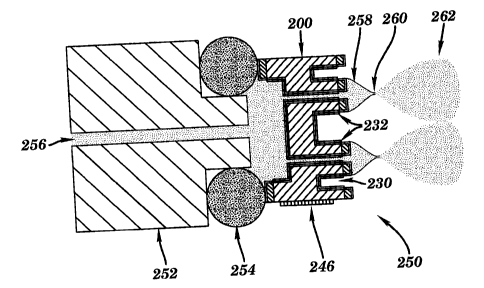
or the like. The perspective view of Figure 4 shows a probe 252 that moves
into
contact with the injection or reservoir side of the electrospray device of the
present
invention. The probe can have a disposable tip. This fluid probe has a seal,
for
example an o-ring 254, at the tip to form a seal between the probe tip and the
injection
surface of the substrate 200. Figure 4 shows an array of a plurality of
electrospray
devices fabricated on a monolithic substrate. One liquid sample handling
device is
shown for clarity, however, multiple liquid sampling devices can be utilized
to
provide one or more fluid samples to one or more electrospray devices in
accordance
with the present invention. The fluid probe and the substrate can be
manipulated in 3-
dimensions for staging of, for example, different devices in front of a mass
spectrometer or other sample detection apparatus.
As shown in Figure 5, to generate an electrospray, fluid may be
delivered to the through-substrate channel 224 of the electrospray device 250
by, for
CA 02395694 2002-06-21
WO 01/50499 PCT/US00/34999
-27-
example, a capillary 256, micropipette or microchip. The fluid is subjected to
a
potential voltage, for example, in the capillary 256 or in the reservoir 242
or via an
electrode provided on the reservoir surface and isolated from the surrounding
surface
region and the substrate 200. A potential voltage may also be applied to the
silicon
substrate via the electrode 246 on the edge of the silicon substrate 200 the
magnitude
of which is preferably adjustable for optimization of the electrospray
characteristics.
The fluid flows through the channel 224 and exits from the nozzle 232 in the
form of
a Taylor cone 258, liquid jet 260, and very fine, highly charged fluidic
droplets 262.
Figure S shows a cross-sectional view of a two-nozzle array of the present
invention.
Figure SA shows a cross-sectional view of a 2 nozzle electrospray device
generating
one electrospray plume from each nozzle for a single fluid stream. Figure SB
shows a
cross-sectional view of a 2 nozzle electrospray device generating 2
electrospray
plumes from each nozzle fox a single fluid stream.
The nozzle 232 provides the physical asperity to promote the formation
of a Taylor cone 258 and efficient electrospray 262 of a fluid 256. The nozzle
232
also forms a continuation of and serves as an exit orifice of the through-
wafer channel
224. The recessed annular region 230 serves to physically isolate the nozzle
232 from
the surface. The present invention allows the optimization of the electric
field lines
emanating from the fluid 256 exiting the nozzle 232, for example, through
independent control of the potential voltage of the fluid 256 and the
potential voltage
of the substrate 200.
Figures 6A - 6D illustrate 1, 2, 3 and 4 electrospray plumes,
respectively, generated from one nozzle 232. Figures 7A - 7B show video
capture
pictures of a microfabricated electrospray device of the present invention
generating
one electrospray plume from one nozzle and two electrospray plumes from one
nozzle, respectively. Figure 8 shows mass spectral results acquired from a
microfabricated electrospray device of the present invention generating from 1
to 4
electrospray plumes from a single nozzle. The applied fluid potential voltage
relative
to the applied substrate potential voltage controls the number of electrospray
plumes
generated. Figure 8A shows the total ion chromatogram ("TIC") of a solution
. containing an analyte at a concentration of 5 ~,M resulting from
electrospray of the
fluid from a microfabricated electrospray device of the present invention. The
substrate voltage for this example is held at zero V while the. fluid voltage
is varied to
CA 02395694 2002-06-21
WO 01/50499 PCT/US00/34999
- 28 -
control the number of electrospray plumes exiting the nozzle. Figure 8B shows
the
selected mass chromatogram for the analyte at m/z 315. In this example, Region
I has
one electrospray plume exiting the nozzle tip with a fluid voltage of 950V.
Region II
has two electrospray plumes exiting the nozzle tip with a fluid voltage of l
OSOV.
S Region III has three electrospray plumes exiting the nozzle tip with a fluid
voltage of
1150 V. Region IV has four electrospray plumes exiting the nozzle tip with a
fluid
voltage of 1250V. Region V has two electrospray plumes exiting the nozzle tip.
Figure 9A shows the mass spectrum resulting from Region I with one
electrospray plume. Figure 9B shows the mass spectrum resulting from Region II
with two electrospray plumes. Figure 9C shows the mass spectrum resulting from
Region III with three electrospray plumes. Figure 9D shows the mass spectrum.
resulting from Region IV with four electrospray plumes exiting the nozzle tip.
It is
clear from the results that this invention can provide an increase in the
analyte
response measured by a mass spectrometer proportional to the number of
electrospray
plumes exiting the nozzle tip. Figure I O charts the ion intensity for m/z 315
for I, 2, 3
and 4 electrospray plumes exiting the nozzle tip.
Figures 11 A -11 C illustrate a system having a two by two array of
electrospray devices. Each device has a group of four electrospray nozzles in
fluid
communication with one common reservoir containing a single fluid sample
source.
Thus, this system can generate multiple sprays for each fluid stream up to
four
different fluid streams.
The electric field at the nozzle tip can be simulated using SIMIONTM
ion optics software. SIMIONTM allows for the simulation of electric field
lines for a
defined array of electrodes. Figure 12A shows a cross-sectional view of a 20
~,m
diameter nozzle 232 with a nozzle height of 50 ~,m. A fluid 256 flowing
through the
nozzle 232 and exiting the nozzle tip in the shape of a hemisphere has a
potential
voltage of 1 OOOV. The substrate 200 has a potential voltage of zero volts. A
simulated third electrode (not shown in the figure due to the scale of the
drawing) is
located 5 mm from the nozzle side of the substrate and has a potential voltage
of zero
volts. This third electrode is generally an ion-sampling orifice of an
atmospheric
pressure ionization mass spectrometer. This simulates the electric field
required for
the formation of a Taylor cone rather than the electric field required to
maintain an
electrospray. Figure I2A shows the equipotential lines in 50 V increments. The
CA 02395694 2002-06-21
WO 01/50499 PCT/US00/34999
- 29 -
closer the equipotential lines are spaced the higher the electric field. The
simulated
electric field at the fluid tip with these dimensions and potential voltages
is
8.2 x 10' Vlm. Figure 12B shows an expanded region around the nozzle of Figure
12A to show greater detail of the equipotential lines. Figure 12C shows the
equipotential lines around this same nozzle with a fluid potential voltage of
1000V,
substrate voltage of zero V and a third electrode voltage of 800 V. The
electric field
at the nozzle tip is 8.0 x 10' V/m indicating that the applied voltage of this
third
electrode has little effect on the electric field at the nozzle tip. Figure
12D shows the
electric field lines around this same nozzle with a fluid potential voltage of
1000V,
substrate voltage of 800 V and a third electrode voltage of 0 V. The electric
field at
the nozzle tip is reduced significantly to a value of 2.2 x 10' V/m. This
indicates that
very fine control of the electric field at the nozzle tip is achieved with
this invention
by independent control of the applied fluid and substrate voltages and is
relatively
insensitive to other electrodes placed up to 5 mm from the device. This level
of
control of the electric field at the nozzle tip is of significant importance
for
electrospray of fluids from a nozzle co-planar with the surface of a
substrate.
This fine control of the electric field allows for precise control of the
electrospray of fluids from these nozzles. When electrospraying fluids from
this
invention, this fine control of the electric field allows fox a controlled
formation of
multiple Taylor cones and electrospray plumes from a single nozzle. By simply
increasing the fluid voltage while maintaining the substrate voltage at zero
V, the
number of electrospray plumes emanating from one nozzle can be stepped from
one
to four as illustrated in Figures 6 and 7.
The high electric f eld at the nozzle tip applies a force to ions
contained within the fluid exiting the nozzle. This force pushes positively-
charged
ions to the fluid surface when a positive voltage is applied to the fluid
relative to the
substrate potential voltage. Due to the repulsive force of likely-charged
ions, the
surface area of the Taylor cone generally defines and limits the total number
of ions
that can reside on the fluidic surface. It is generally believed that, for
electrospray, a
gas phase ion for an analyte can most easily be formed by that analyte when it
resides
on the surface of the fluid. The total surface area of the fluid increases as
the number
of Taylor cones at the nozzle tip increases resulting in the increase in
solution phase
ions at the surface of the fluid prior to electrospray formation. The ion
intensity will
CA 02395694 2002-06-21
WO 01/50499 PCT/US00/34999
-30-
increase as measured by the mass spectrometer when the number of electrospray
plumes increase as shown in the example above.
Another important feature of the present invention is that since the
electric field around each nozzle is preferably defined by the fluid and
substrate
voltage at the nozzle tip, multiple nozzles can be located in close proximity,
on the
order of tens of microns. This novel feature of the present invention allows
for the
formation of multiple electxospray plumes from multiple nozzles of a single
fluid
stream thus greatly increasing the electrospray sensitivity available for
microchip-
based electrospray devices. Multiple nozzles of an electrospray device in
fluid
communication with one another not only improve sensitivity but also increase
the
flow rate capabilities of the device. For example, the flow rate of a single
fluid stream
through one nozzle having the dimensions of a 10 micron inner diameter, 20
micron
outer diameter, and a 50 micron length is about 1 ~,L/min.; and the flow rate
through
200 of such nozzles is about 200 ~,L/min. Accordingly, devices can be
fabricated
having the capacity for flow rates up to about 2 ~,L/min., from about 2
qL/min. to
about 1 mL/min., from about 100 nL/min. to about 500 nL/min., and greater than
about 2 ~,Llmin. possible.
Arrays of multiple electrospray devices having any nozzle number and
format may be fabricated according to the present invention. The electrospray
devices can be positioned to form from a low-density array to a high-density
axray of
devices. Arrays can be provided having a spacing between adjacent devices of 9
mm,
4.5 mm, 2.25 mm, 1.12 mm, 0.56 mm, 0.28 mm, and smaller to a spacing as close
as
about 50 ~,m apart, respectively, which correspond to spacing used in
commercial
instrumentation for liquid handling or accepting samples from electrospray
systems.
Similarly, systems of electrospray devices can be fabricated in an array
having a
device density exceeding about 5 devices/cm2, exceeding about 16 devices/cm2,
exceeding about 30 devices/cm2, and exceeding about 81 devices/cm2, preferably
from about 30 devices/cm2 to about 100 devices/cm2.
Dimensions of the electrospray device can be determined according to
various factors such as the specific application, the layout design as well as
the
upstream and/or downstream device to which the electrospray device is
interfaced or
integrated. Further, the dimensions of the channel and nozzle may be optimized
for
CA 02395694 2002-06-21
WO 01/50499 PCT/US00/34999
-31 -
the desired flow rate of the fluid sample. The use of reactive-ion etching
techniques
allows for the reproducible and cost effective production of small diameter
nozzles,
for example, a 2 ~,m inner diameter and 5 ~,m outer diameter. Such nozzles can
be
fabricated as close as 20 ~m apart, providing a density of up to about 160,000
nozzles/cm2. Nozzle densities up to about 10,000/cm2, up to about 15,625/cm2,
up to
about 27,566/cm2, and up to about 40,000/cm2, respectively, can be provided
within
an electrospay device. Similarly, nozzles can be provided wherein the spacing
on the
ejection surface between the centers of adjacent exit orifices of the spray
units is less
than about 500 ~,m, less than about 200 Vim, less than about 100 ~.m, and less
than
about 50 ~,m, respectively. For example, an electrospray device having one
nozzle
with an outer diameter of 20 ~,m would respectively have a surrounding sample
well
30 ~m wide. A densely packed array of such nozzles could be spaced as close as
50
~,m apart as measured from the nozzle center.
In one currently preferred embodiment, the silicon substrate of the
electrospray device is approximately 250-500 ~,rn in thickness and the cross-
sectional
area of the through-substrate channel is less than approximately 2,500 ~,m2.
Where
the channel has a circular cross-sectional shape, the channel and the nozzle
have an
inner diameter of up to 50 pm, more preferably up to 30 pm; the nozzle has an
outer
diameter of up to 60 ~,m, more preferably up to 40 p,m; and nozzle has a
height of
(and the annular region has a depth of) up to 100 Vim. The recessed portion
preferably
extends up to 300 ~,m outwardly from the nozzle. The silicon dioxide layer has
a
thickness of approximately 1-4 ~,m, preferably 1-3 Vim. The silicon nitride
layer has a
thickness of approximately less than 2 ~,m.
Furthermore, the electrospray device may be operated to produce
larger, minimally-charged droplets. This is accomplished by decreasing the
electric
field at the nozzle exit to a value less than that required to generate an
electrospray of
a given fluid. Adjusting the ratio of the potential voltage of the fluid and
the potential
voltage of the substrate controls the electric field. A fluid to substrate
potential
voltage ratio approximately less than 2 is preferred for droplet formation.
The droplet
diameter in this mode of operation is controlled by the fluid surface tension,
applied
voltages and distance to a droplet receiving well or plate. This mode of
operation is
ideally Baited for conveyance and/or apportionment of a multiplicity of
discrete
CA 02395694 2002-06-21
WO 01/50499 PCT/US00/34999
-32-
amounts of fluids, and may find use in such devices as ink jet printers and
equipment
and instruments requiring controlled distribution of fluids.
The electrospray device of the present invention includes a silicon
substrate material defining a channel between an entrance orifice on a
reservoir
surface and a nozzle on a nozzle surface such that the electrospray generated
by the
device is generally perpendicular to the nozzle surface. The nozzle has an
inner and
an outer diameter and is defined by an annular portion recessed from the
surface. The
recessed ammlax region extends radially from the nozzle outer diameter. The
tip of
the nozzle is co-planar or level with and preferably does not extend beyond
the
substrate surface. In this manner the nozzle can be protected against
accidental
breakage. The nozzle, channel, reservoir and the recessed annular region are
etched
from the silicon substrate by reactive-ion etching and other standard
semiconductor
processing techniques.
All surfaces of the silicon substrate preferably have insulating layers to
electrically isolate the liquid sample from the substrate such that different
potential
voltages may be individually applied to the substrate and the liquid sample.
The
insulating layers can constitute a silicon dioxide layer combined with a
silicon nitride
layer. The silicon nitride layer provides a moisture barrier against water and
ions
from penetrating through to the substrate causing electrical breakdown between
a
fluid moving in the channel and the substrate. The electrospray apparatus
preferably
includes at Ieast one controlling electrode electrically contacting the
substrate for the
application of an electric potential to the substrate.
Preferably, the nozzle, channel and recess are etched from the silicon
substrate by reactive-ion etching and other standard semiconductor processing
techniques. The nozzle side features, through-substrate fluid channel,
reservoir side
features, and controlling electrodes are preferably formed monolithically from
a
monocrystalline silicon substrate -- i.e., they are formed during the course
of and as a
result of a fabrication sequence that requires no manipulation or assembly of
separate
components.
Because the electrospray device is manufactured using reactive-ion
etching and other standard semiconductor processing techniques, the dimensions
of
such a device can be very small, for example, as small as 2 ~,m inner diameter
and
5 ~.m outer diameter. Thus, a through-substrate fluid channel having, for
example,
CA 02395694 2002-06-21
WO 01/50499 PCT/US00/34999
-33-
p,m inner diameter and a substrate thickness of 250 p,m only has a volume of
4.9 pL.
The micrometer-scale dimensions of the electrospray device minimize the dead
volume and thereby increase efficiency and analysis sensitivity when combined
with a
separation device.
The electrospray device of the present invention provides for the
efficient and effective formation of an electrospray. By providing an
electrospray
surface from which the fluid is ejected with dimensions on the order of
micrometers,
the electrospray device limits the voltage required to generate a Taylor cone
as the
voltage is dependent upon the nozzle diameter, the surface tension of the
fluid, and
the distance of the nozzle from an extracting electrode. The nozzle of the
electrospray
device provides t'he physical asperity on the order of micrometers on which a
large
electric field is concentrated. Further, the electrospray device may provide
additional
electrodes) on the ejecting surface to which electric potentials) may be
applied and
controlled independent of the electric potentials of the fluid and the
extracting
electrode in order to advantageously modify and optimize the electric field in
order to
focus the gas phase ions resulting from electrospray of fluids. The
combination of the
nozzle and the additional electrodes) thus enhance the electric field between
the
nozzle, the substrate and the extracting electrode. The electrodes are
preferable
positioned within about 500 microns, and more preferably within about 200
microns
from the exit orifice.
The microchip-based electrospray device of the present invention
provides minimal extra-column dispersion as a result of a reduction in the
extra-
column volume arid provides efficient, reproducible, reliable and rugged
formation of
an electrospray. This electrospray device is perfectly suited as a means of
electrospray of fluids from microchip-based separation devices. The design of
this
electrospray device is also robust such that the device can be readily mass-
produced
in a cost-effective, high-yielding process.
In operation, a conductive or partly conductive liquid sample is
introduced into the through-substrate channel entrance orifice on the
injection surface.
The liquid is held at a potential voltage, either by means of a conductive
fluid delivery
device to the electrospray device or by means of an electrode formed on the
injection
surface isolated from the surrounding surface region and from the substrate.
The
electric field strength at the tip of the nozzle is enhanced by the
application of a
CA 02395694 2002-06-21
WO 01/50499 PCT/US00/34999
-34-
voltage to the substrate and/or the ejection surface, preferably zero volts up
to
approximately less than one-half of the voltage applied to the fluid. Thus, by
the
independent control of the fluid/nozzle and substrate/ejection surface
voltages, the
electrospray device of the present invention allows the optimization of the
electric
field emanating from the nozzle. The electrospray device of the present
invention
may be placed 1-2 ruin or up to 10 mm from the orifice of an atmospheric
pressure
ionization ("API") mass spectrometer to establish a stable nanoelectrospray at
flow
rates in the range of a few nanoliters per minute.
The electrospray device may be interfaced or integrated downstream to
a sampling device, depending on the particular application. For example, the
analyte
may be electrosprayed onto a surface to coat that surface or into another
device for
purposes of conveyance, analysis, and/or synthesis. As described above, highly
charged droplets are formed at atmospheric pressure by the electrospray device
from
nanoliter-scale volumes of an analyte. The highly charged droplets produce gas-
phase
ions upon sufficient evaporation of solvent molecules which may be sampled,
for
example, through an ion-sampling orifice of an atmospheric pressure ionization
mass
spectrometer ("API-MS") for analysis of the electrosprayed fluid.
One embodiment of the present invention is in the form of an array of
multiple electrospray devices which allows for massive parallel processing.
The
multiple electrospray devices or systems fabricated by massively parallel
processing
on a single wafer may then be cut or otherwise separated into multiple devices
or
. systems.
The electrospray device may also serve to reproducibly distribute and
deposit a sample from a mother plate to daughter plates) by nanoelectrospray
deposition or by the droplet method. A chip-based combinatorial chemistry
system
including a reaction well block may define an array of reservoirs for
containing the
reaction products from a combinatorially synthesized compound. The reaction
well
block further defines channels, nozzles and recessed portions such that the
fluid in
each reservoir may flow through a corresponding channel and exit through a
corresponding nozzle in the form of droplets. The reaction well block may
define any
number of reservoirs) in any desirable configuration, each reservoir being of
a
suitable dimension and shape. The volume of a reservoir may range from a few
picoliters up to several microliters.
CA 02395694 2002-06-21
WO 01/50499 PCT/US00/34999
-35-
The reaction well block may serve as a mother plate to interface to a
microchip-based chemical synthesis apparatus such that the droplet method of
the
electrospray device may be utilized to reproducibly distribute discreet
quantities of
the product solutions to a receiving or daughter plate. The daughter plate
defines
receiving wells that correspond to each of the reservoirs. The distributed
product
solutions in the daughter plate may then be utilized to screen the
combinatorial
chemical library against biological targets.
The electrospray device may also serve to reproducibly distribute and
deposit an array of samples from a mother plate to daughter plates, for
example, for
proteomic screening of new drug candidates. This may be by either droplet
formation
or electrospray modes of operation. Electrospray devices) may be etched into a
microdevice capable of synthesizing combinatorial chemical libraries. At a
desired
time, a nozzles) may apportion a desired amount of a samples) or reagents)
from a
mother plate to a daughter plate(s). Control of the nozzle dimensions, applied
voltages, and time provide a precise and reproducible method of sample
apportionment or deposition from an array of nozzles, such as for the
generation of
sample plates for molecular weight determinations by matrix-assisted laser
desorption/ionization time-of flight mass spectrometry ("MALDI-TOFMS"). The
capability of transferring analytes from a mother plate to daughter plates may
also be
utilized to make other daughter plates for other types of assays, such as
proteomic
screening. The fluid to substrate potential voltage xatio can be chosen fox
formation
of an electrospray or droplet mode based on a particular application.
An array of multiple electrospray devices can be configured to disperse
ink for use in an ink jet printer. The control and enhancement of the electric
field at
the exit of the nozzles on a substrate will allow for a variation of ink
apportionment
schemes including the formation of droplets approximately two times the nozzle
diameters or of submicometer, highly-charged droplets for blending of
different
colors of ink.
The electrospray device of the present invention can be integrated with
miniaturized liquid sample handling devices for efficient electrospray of the
liquid
samples for detection using a mass spectrometer. The electrospray device may
also
be used to distribute and apportion fluid samples for use with high-throughput
screen
technology. The electrospray device may be chip-to-chip or wafer-to-wafer
bonded to
CA 02395694 2002-06-21
WO 01/50499 PCT/US00/34999
-36-
plastic, glass, or silicon microchip-based liquid separation devices capable
of, for
example, capillary electrophoresis, capillary electrochromatography, affinity
chromatography, liquid chromatography ("LC"), or any other condensed-phase
separation technique.
An array or matrix of multiple electrospray devices of the present
invention may be manufactured on a single microchip as silicon fabrication
using
standard, well-controlled thin-film processes. This not only eliminates
handling of
such micro components but also allows for rapid parallel processing of
functionally
similar elements. The low cost of these electrospray devices allows for one-
time use
such that cross-contamination from different liquid samples may be eliminated.
Figures 13A -13E illustrate the deposition of a discreet sample onto
an electrospray device of the present invention. Figures 13A -13C show a
fluidic
probe depositing or transferring a sample to a reservoir on the injection
surface. The
fluidic sample is delivered to the reservoir as a discreet volume generally
less than
100 nL. ~ The 'dots' represent analytes contained within a fluid. Figure 13D
shows the
fluidic sample volume evaporated leaving the analytes on the reservoir
surface. This
reservoir surface may be coated with a retentive phase, such as a hydrophobic
C18-like phase commonly used for LC applications, for increasing the partition
of
analytes contained within the fluid to the reservoir surface. Figure 13E shows
a
fluidic probe sealed against the injection surface to deliver a fluidic mobile
phase to
the microchip to reconstitute the transferred analytes for analysis by
electrospray mass
spectrometry. The probe can have a disposable tip, such as a capillary,
micropipette,
or microchip.
A mufti-system chip thus provides a rapid sequential chemical analysis
system fabricated using Micro-ElectroMechanical System ("MEMS") technology.
For example, the mufti-system chip enables automated, sequential separation
and
injection of a multiplicity of samples, resulting in significantly greater
analysis
throughput and utilization of the mass spectrometer instrument fox, for
example, high-
throughput detection of compounds for drug discovery.
Another aspect of the present invention provides a silicon microchip-
based electrospray device for producing electrospray of a liquid sample. The
electrospray device may be interfaced downstream to an atmospheric pressure
ionization mass spectrometer ("API-MS") for analysis of the electrosprayed
fluid.
CA 02395694 2002-06-21
WO 01/50499 PCT/US00/34999
-37-
Another aspect of the invention is an integrated miniaturized liquid phase
separation
device, which may have, for example, glass, plastic or silicon substrates
integral with
the electrospray device.
Electrospray Device Fabrication Procedure
The electrospray device 250 is preferably fabricated as a monolithic
silicon substrate utilizing well-established, controlled thin-film silicon
processing
techniques such as thermal oxidation, photolithography, reactive-ion etching
(RIE),
chemical vapor deposition, ion implantation, and metal deposition. Fabrication
using
such silicon processing techniques facilitates massively parallel processing
of similar
devices, is time- and cost-efficient, allows for tighter control of critical
dimensions, is
easily reproducible, and results in a wholly integral device, thereby
eliminating any
assembly requirements. Further, the fabrication sequence may be easily
extended to
create physical aspects or features on the injection surface and/or ejection
surface of
the electrospray device to facilitate interfacing and connection to a fluid
delivery
system or to facilitate integration with a fluid delivery sub-system to create
a single
integrated system.
Nozzle Surface Processing:
Figures 14A - 14E and Figures 1 SA - 1 SI illustrate the processing
steps for the nozzle or ejection side of the substrate in fabricating the
electrospray
device of the present invention. Referring to the plan view of Figure 14A, a
mask is
used to pattern 202 that will form the nozzle shape in the completed
electrospray
device 250. The patterns in the form of circles 204 and 206 forms through-
wafer
channels and a recessed annular space around the nozzles, respectively of a
completed
electrospray device. Figure 14B is the cross-sectional view taken along line
14B-14B
of Figure 14A. A double-side polished silicon wafer 200 is subjected to an
elevated
temperature in an oxidizing environment to grow a layer or film of silicon
dioxide 210
on the nozzle side and a layer or f lm of silicon dioxide 212 on the reservoir
side of
the substrate 200. Each of the resulting silicon dioxide layers 210, 212 has a
thickness of approximately 1-3 Vim. The silicon dioxide layers 210, 212 serve
as
masks for subsequent selective etching of certain areas of the silicon
substrate 200.
CA 02395694 2002-06-21
WO 01/50499 PCT/US00/34999
-38-
A film of positive-working photoresist 208 is deposited on the silicon
dioxide layer 210 on the nozzle side of the substrate 200. Referring to Figure
14C, an
area of the photoresist 204 corresponding to the entrance to through-wafer
channels
and an area of photoresist corresponding to the recessed annular region 206
which
will be subsequently etched is selectively exposed through a mask (Figure 14A)
by an
optical lithographic exposure tool passing short-wavelength light, such as
blue or
near-ultraviolet at wavelengths of 365, 405, or 436 nanometers.
As shown in the cross-sectional view of Figure 14C, after development
of the photoresist 208, the exposed area 204 of the photoresist is removed and
open to
the underlying silicon dioxide layer 214 and the exposed area 206 of the
photoresist is
removed and open to the underlying silicon dioxide layer 216, while the
unexposed
areas remain protected by photoresist 208. Referring to Figure 14D, the
exposed
areas 214, 216 of the silicon dioxide layer 210 is then etched by a fluorine-
based
plasma with a high degree of anisotropy and selectivity to the protective
photoresist
208 until the silicon substrate 218, 220 are reached. As shown in the cross-
sectional
view of Figure 14E, the remaining photoresist 208 is removed from the silicon
substrate 200.
Referring to the plan view of Figure 15A, a mask is used to pattern 204
in the form of circles. Figure 1 SB is the cross-sectional view taken along
line 15B-
15B of Figure 15A. A film of positive-working photoresist 208' is deposited on
the
silicon dioxide layer 210 on the nozzle side of the substrate 200. Referring
to Figure
15C, an area of the photoresist 204 corresponding to the entrance to through-
wafer
channels is selectively exposed through a mask (Figure 15A) by an optical
lithographic exposure tool passing short-wavelength light, such as blue or
near-
ultraviolet at wavelengths of 365, 405, or 436 nanometers.
As shown in the cross-sectional view of Figure 15C, after development
of the photoresist 208', the exposed area 204 of the photoresist is removed to
the
underlying silicon substrate 218. The remaining photoresist 208' is used as a
mask
during the subsequent fluorine based DRIE silicon etch to vertically etch the
through-
wafer channels 224 shown in Figure 15D. After etching the through-wafer
channels
224, the remaining photoresist 208' is removed from the silicon substrate 200.
As shown in the cross-sectional view of Figure 15E, the removal of the
photoresist 208' exposes the mask pattern of Figure 14A formed in the silicon
dioxide
CA 02395694 2002-06-21
WO 01/50499 PCT/US00/34999
-39-
210 as shown in Figurel4E. Referring to Figure 15F, the silicon wafer of
Figure 15E
is subjected to an elevated temperature in an oxidizing environment to grow a
layer or
film of silicon dioxide 226, 228 on all exposed silicon surfaces of the wafer.
Referring to Figure 15G, the silicon dioxide 226 is then etched by a fluorine-
based
plasma with a high degree of anisotropy and selectivity until the silicon
substrate 220
is reached. The silicon dioxide layer 228 is designed to serve as an etch stop
during
the DRIE etch of Figure 15H that is used to form the nozzle 232 and recessed
annular
region 230.
An advantage of the fabrication process described herein is that the
process simplifies the alignment of the through-wafer channels and the
recessed
annular region. This allows the fabrication of smaller nozzles with greater
ease
without any complex alignment of masks. Dimensions of the through channel,
such
as the aspect ratio (i.e.. depth to width), can be reliably and reproducibly
limited and
controlled.
Reservoir Surface Processing:
Figures 16A - 16I illustrate the processing steps for the reservoir or
injection side of the substrate 200 in fabricating the electrospray device 250
of the
present invention. As shown in the cross-sectional view in Figure 16B (a cross-
sectional view taken along line 16B-16B of Figure 16A), a film of positive-
working
photoresist 236 is deposited on the silicon dioxide layer 212. Patterns on the
reservoir
side are aligned to those previously formed on the nozzle side of the
substrate using
through-substrate alignments.
After alignment, an area of the photoresist 236 corresponding to the
circular reservoir 234 is selectively exposed through a mask (Figure 16A) by
an
optical lithographic exposure tool passing short-wavelength light, such as
blue or
near- ultraviolet at wavelengths of 365, 405, or 436 nanometers. As shown in
the
cross-sectional view of Figure 16C, the photoresist 236 is then developed to
remove
the exposed areas of the photoresist 234 such that the reservoir region is
open to the
underlying silicon dioxide layer 238, while the unexposed areas remain
protected by
photoresist 236. The exposed area 238 of the silicon dioxide layer 212 is then
etched
by a fluorine-based plasma with a high degree of anisotropy and selectivity to
the
CA 02395694 2002-06-21
WO 01/50499 PCT/US00/34999
-40-
protective photoresist 236 until the silicon substrate 240 is reached as shown
in Figure
16D.
As shown in Figure 16E, a fluorine-based etch creates a cylindrical
region that defines a reservoir 242. The reservoir 242 is etched until the
through-
wafer channels 224 are reached. After the desired depth is achieved the
remaining
photoresist 236 is then removed in an oxygen plasma or in an actively
oxidizing
chemical bath like sulfuric acid (HZS04) activated with hydrogen peroxide
(H202), as
shown in Figure 16F.
Preparation of the Substrate for Electrical Isolation
Referring to Figure 16G, the silicon wafer 200 is subjected to an
elevated temperature in an oxidizing environment to grow a layer or film of
silicon
dioxide 244 on all silicon surfaces to a thickness of approximately 1-3 ~,m.
The
silicon dioxide layer serves as an electrical insulating layer. Silicon
nitride 246 is
further deposited using low pressure chemical vapor deposition (LPCVD) to
provide a
conformal coating of silicon nitride on all surfaces up to 2 ~,m in thickness,
as shown
in Figure 16H. LPCVD silicon nitride also provides further electrical
insulation and a
fluid barrier that prevents fluids and ions contained therein that are
introduced to the
electrospray device from causing an electrical connection between.the fluid
the silicon
substrate 200. This allows for the independent application of a potential
voltage to a
fluid and the substrate with this electrospray device to generate the high
electric field
at the nozzle tip required for successful nanoelectrospray of fluids from
microchip
devices.
After fabrication of multiple electrospray devices on a single silicon
wafer, the wafer can be diced or cut into individual devices. This exposes a
portion of
the silicon substrate 200 as shown in the cross-sectional view of Figure 16I
on which
a layer of conductive metal 24~ is deposited.
All silicon surfaces are oxidized to form silicon dioxide with a
thickness that is controllable through choice of temperature and time of
oxidation. All
silicon dioxide surfaces are LPCVD coated with silicon nitride. The final
thickness of
the silicon dioxide and silicon nitride can be selected to provide the desired
degree of
electrical isolation in the device. A thicker layer of silicon dioxide and
silicon nitride
provides a greater resistance to electrical breakdown. The silicon substrate
is divided
CA 02395694 2002-06-21
WO 01/50499 PCT/US00/34999
-41 -
into the desired size or array of electrospray devices for purposes of
metalization of
the edge of the silicon substrate. As shown in Figure 16I, the edge of the
silicon
substrate 200 is coated with a conductive material 248 using well known
thermal
evaporation and metal deposition techniques.
The fabrication method confers superior mechanical stability to the
fabricated electrospray device by etching the features of the electrospray
device from
a monocrystalline silicon substrate without any need for assembly. The
alignment
scheme allows for nozzle walls of less than 2 ~,m and nozzle outer diameters
down to
~,m to be fabricated reproducibly. Further, the lateral extent and shape of
the
recessed annular region can be controlled independently of its depth. The
depth of the
recessed annular region also determines the nozzle height and is determined by
the
extent of etch on the nozzle side of the substrate.
The above described fabrication sequence for the electrospray device
can be easily adapted to and is applicable for the simultaneous fabrication of
a single
monolithic system comprising multiple electrospray devices including multiple
channels and/or multiple ejection nozzles embodied in a single monolithic
substrate.
Further, the processing steps may be modified to fabricate similar ar
different
electrospray devices merely by, for example, modifying the layout design
and/or by
changing the polarity of the photomask and utilizing negative-working
photoresist
rather than utilizing positive-working photoresist.
In a further embodiment an alternate fabrication technique is set forth
in Figures 17 - 20. This technique has several advantages over the prior
technique,
primarily due to the function of the etch stop deposited on the reservoir side
of the
substrate. This feature improves the production of through-wafer channels
having a
25~ consistent diameter throughout its length. An artifact of the etching
process is the
difficulty of maintaining consistent channel diameter when approaching an
exposed
surface of the substrate from within. Typically, the etching process forms a
channel
having a slightly smaller diameter at the end of the channel as it breaks
through the
opening. This is improved by the ability to slightly over-etch the channel
when
contacting the etch stop. Further, another advantage of etching the reservoir
and
depositing an etch stop prior to the channel etch is that micro-protrusions
resulting
from the side passivation of the channels remaining at the channel opening are
avoided. The etch stop also functions to isolate the plasma region from the
cooling
CA 02395694 2002-06-21
WO 01/50499 PCT/US00/34999
-42-
gas when providing through holes and avoiding possible contamination from
etching
by products.
Figures 17A - 17E and Figures 19A -19G illustrate the processing
steps for the nozzle or ejection side of the substrate in fabricating the
electrospray
device of the present invention. Figures 18A - 18G illustrate the processing
steps for
the reservoir or injection side of the substrate in fabricating the
electrospray device of
the present invention. Figures 20A - 20C illustrate the preparation of the
substrate for
electrical isolation.
Referring to the plan view of Figure 17A, a mask is used to pattern 302
that will form the nozzle shape in the completed electrospray device 250. The
patterns in the form of circles 304 and 306 forms through-wafer channels and a
recessed annular space around the nozzles, respectively of a completed
electrospray
device. Figure I7B is the cross-sectional view taken along line 17B-17B of
Figure
17A. A double-side polished silicon wafer 300 is subjected to an elevated
temperature in an oxidizing environment to grow a layer or film of silicon
dioxide 310
on the nozzle side and a layer or film of silicon dioxide 312 on the reservoir
side of
the substrate 300. Each of the resulting silicon dioxide layers 310, 312 has a
thickness of approximately 1-3 ~,m. The silicon dioxide layers 310, 312 serve
as
masks for subsequent selective etching of certain areas of the silicon
substrate 300.
A film of positive-working photoresist 308 is deposited on the silicon
dioxide layer 310 on the nozzle side of the substrate 300. Referring to Figure
17C, an
area of the photoresist 304 corresponding to the entrance to through-wafer
channels
and an area of photoresist corresponding to the recessed annular region 306
which
will be subsequently etched is selectively exposed through a mask (Figure 17A)
by an
optical lithographic exposure tool passing short-wavelength light, such as
blue or
near-ultraviolet at wavelengths of 365, 405, or 436 nanometers.
As shown in the cross-sectional view of Figure 17C, after development
of the photoresist 308, the exposed area 304 of the photoresist is removed and
open to
the underlying silicon dioxide layer 314 and the exposed area 306 ofthe
photoresist is
removed and open to the underlying silicon dioxide layer 310, while the
unexposed
areas remain protected by photoresist 308. Referring to Figure 17D, the
exposed
areas 314, 316 of the silicon dioxide layer 310 is then etched by a fluorine-
based
plasma with a high degree of anisotropy and selectivity to the protective
photoresist
CA 02395694 2002-06-21
WO 01/50499 PCT/US00/34999
- 43 -
308 until the silicon substrate 318, 320 are reached. As shown in the cross-
sectional
view of Figure 17E, the remaining photoresist 308 is xemoved from the silicon
substrate 300.
Referring to the plan view of Figure 18A, a mask is used to pattern 324
in the form of a circle. Figure 18B is the cross-sectional view taken along
line 18B-
18B of Figure 18A. As shown in the cxoss-sectional view in Figure 18B a film
of
positive-working photoresist 326 is deposited on the silicon dioxide layer
312.
Patterns on the reservoir side are aligned to those previously formed on the
nozzle
side of the substrate using through-substrate alignments.
After alignment, an area of the photoresist 326 corresponding to the
circular reservoir 324 is selectively exposed through the mask (Figure 18A) by
an
optical lithographic exposure tool passing short-wavelength light, such as
blue or
near-ultraviolet at wavelengths of 365, 405, or 436 nanometers. As.shown in
the
cross-sectional view of Figure 18C, the photoresist 326 is then developed to
remove
the exposed areas of the photoresist 324 such that the reservoir region is
open to the
underlying silicon dioxide layer 328, while the unexposed areas remain
protected by
photoresist 326. The exposed area 328 of the silicon dioxide layer 312 is then
etched
by a,fluorine-based plasma with a high degree of anisotropy and selectivity to
the
protective photoresist 326 until the silicon substrate 330 is xeached as shown
in Figure
18D.
As shown in Figure 18E, a fluorine-based etch creates a cylindrical
region that defines a reservoir 332. The reservoir 332 is etched until the
through-
wafer channel depths are reached. After the desired depth is achieved the
remaining
photoresist 326 is then removed in an oxygen plasma or in an actively
oxidizing
chemical bath like sulfuric acid (H2S04) activated with hydrogen peroxide
(H202); as
shown in Figure 18F.
Referring to Figure 18G, a plasma enhanced chemical vapor deposition
("PECVD") silicon dioxide layer 334 is deposited on the reservoir side of the
substrate 300 to serve as an etch stop for the subsequent etch of the through
substrate
channel 336 shown in Figure 19D.
A film of positive-working photoxesist 308' is deposited on the silicon
dioxide layer 310 on the nozzle side of the substrate 300, as shown in Figure
19B.
Referring to Figure 19C, an area of the photoresist 304 corresponding to the
entrance
CA 02395694 2002-06-21
WO 01/50499 PCT/US00/34999
-44-
to through-wafer channels is selectively exposed through a mask (Figure 19A)
by an
optical lithographic exposure tool passing short-wavelength light, such as
blue or
near-ultraviolet at wavelengths of 365, 405, or 436 nanometers.
As shown in the cross-sectional view of Figure 19C, after development
of the photoresist 308', the exposed area 304 of the photoresist is removed to
the
underlying silicon substrate 318. The remaining photoresist 308' is used as a
mask
during the subsequent fluorine based DRIE silicon etch to vertically etch the
through-
wafer channels 336 shown in Figure 19D. After etching the through-wafer
channels
336, the remaining photoresist 308' is removed from the silicon substrate 300,
as
shown in the cross-sectional view of Figure 19E.
The removal of the photoresist 308' exposes the mask pattern of Figure
17A formed in the silicon dioxide 310 as shown in Figure 19E. The fluorine
based
DRIE silicon etch is used to vertically etch the recessed annular region 338
shown in
Figure 19F. Referring to Figure 19G, the silicon dioxide layers 310, 312 and
334 are
removed from the substrate by a hydrofluoric acid process.
An advantage of the fabrication process described herein is that the
process simplifies the alignment of the through-wafex channels and the
recessed
annular region. This allows the fabrication of smaller nozzles with greater
ease
without any complex alignment of masks. Dimensions of the through channel,
such
as the aspect ratio (i.e. depth to width), can be reliably and reproducibly
Limited and
controlled.
Preparation of the Substrate for Electrical Isolation
Referring to Figure 20A, the silicon wafer 300 is subjected to an
elevated temperature in an oxidizing environment to grow a layer or film of
silicon
dioxide 342 on all silicon surfaces to a thickness of approximately 1-3 ~.m.
The
silicon dioxide Layer serves as an electrical insulating layer. Silicon
nitride 344 is
further deposited using low pressure chemical vapor deposition (LPCVD) to
provide a
conformal coating of silicon nitride on all surfaces up to 2 ~,m in thickness,
as shown
in Figure 20B. LPCVD silicon nitride also provides further electrical
insulation and a
fluid barrier that prevents fluids and ions contained therein that are
introduced to the
electrospray device from causing an electrical connection between the fluid
the silicon
substrate 300. This allows for the independent application of a potential
voltage to a
CA 02395694 2002-06-21
WO 01/50499 PCT/US00/34999
- 45 -
fluid and the substrate with this electrospray device to generate the high
electric field
at the nozzle tip required for successful nanoelectrospray of fluids from
microchip
devices.
After fabrication of multiple electrospray devices on a single silicon
wafer, the wafer can be diced or cut into individual devices. This exposes a
portion of
the silicon substrate 300 as shown in the cross-sectional view of Figure 20C
on which
a layer of conductive metal 346 is deposited, which serves as the substrate
electrode.
A layer of conductive metal 348 is deposited on the silicon nitride layer of
the
reservoir side, which serves as the fluid electrode.
All silicon surfaces are oxidized to form silicon dioxide with a
thickness that is controllable through choice of temperature and time of
oxidation. All
silicon dioxide surfaces are LPCVD coated with silicon nitride. The final
thickness of
the silicon dioxide and silicon nitride can be selected to provide the desired
degree of
electrical isolation in the device. A thicker Layer of silicon dioxide and
silicon nitride
provides a greater resistance to electrieal'breakdown. The silicon substrate
is divided
into the desired size or array of electrospray devices for purposes of
metalization of
the edge of the silicon substrate. As shown in Figure 20C, the edge of the
silicon .
substrate 300 is coated with a conductive material 248 using well known
thermal
evaporation and metal deposition techniques.
The fabrication methods confer superior mechanical stability to the
fabricated electrospray device by etching the features of the electrospray
device from
a monocrystalline silicon substrate without any need for assembly. The
alignment
scheme allows for nozzle walls of less than 2 ~,m and nozzle outer diameters
down to
5 ~m to be fabricated reproducibly. Further, the lateral extent and shape of
the
recessed annular region can be controlled independently of its depth. The
depth of the
recessed annular region also determines the nozzle height and is determined by
the
extent of etch on the nozzle side of the substrate.
Figures 21A and 21B show a perspective view of scanning electron
micrograph images of a mufti-nozzle device fabricated in accordance with the
present
invention. The nozzles have a 20 ~,m outer diameter and an 8 ~m inner
diameter.
The pitch, which is the nozzle center to nozzle center spacing of the nozzles
is 50 p,m.
CA 02395694 2002-06-21
WO 01/50499 PCT/US00/34999
-46-
The above described fabrication sequences for the electrospray device
can be easily adapted to and axe applicable for the simultaneous fabrication
of a single
monolithic system comprising multiple electrospray devices including multiple
channels and/or multiple ejection nozzles embodied in a single monolithic
substrate.
Further, the processing steps may be modified to fabricate similar or
different
electrospray devices merely by, for example, modifying the layout design
and/or by
changing the polarity of the photomask and utilizing negative-working
photoresist
rather than utilizing positive-working photoresist.
Interface of a Multi-System Chip to a Mass Spectrometer
Arrays of electrospray nozzles on a mufti-system chip may be
interfaced with a sampling orifice of a mass spectrometer by positioning the
nozzles
near the sampling orifice. The tight configuration of electrospray nozzles
allows the
positioning thereof in close proximity to the sampling orifice of a mass
spectrometer.
A mufti-system chip may be manipulated relative to the ion sampling
orifice to position one or more of the nozzles for electrospray near the
sampling
orifice. Appropriate voltages) may then be applied to the one or more of the
nozzles
fox electrospray.
Although the invention has been described in detail for the purpose of
illustration, it is understood that such detail is solely for that purpose,
and variations
can be made therein by those skilled in the art without departing from the
spirit and
scope of the invention which is defined by the following claims.