Note: Descriptions are shown in the official language in which they were submitted.
CA 02395760 2002-06-21
WO 01/47003 PCT/US00/35139
METHODS AND APPARATUS FOR f~ORMING SUBMICRON PATTERNS ON FILMS
Cross-Refi:rence to Related Application
This application claims benefit from U. S. provision application 60/173,001,
filed on
December 23, 1999, which is incorporated herein by reference in its entirety.
Field of the Invention
The invention relates to methods and apparatus for producing submicron
patterns on
films. This invention was made with government support under NSF #DMR-9809365,
and
DOE #DE-FG02--96ER45612. The government has certain rights in this invention.
Background of the Invention
In the microelectronics, biotechnology, adhesive, and microsystem industries,
it is
important to produce high-resolution patterns on substrates. For examples,
such high-
resolution patterns are necessary to produce integrated circuits. Limits on
the resolution of
such patterns limit the performance of such integrated circuits. Presently,
1111CI'Olltl70g1'aphV
is commonly used to produce patterns on substrates. Microlithography
techniques involve
exposing a photoresist to an optical pattern, and using chemicals to etch
either the exposed,
or unexposed, portions of the photoresist to produce the pattern on the
substrate. The
resolution of the pattern is thus limited by the wavelength of light used to
produce the optical
pattern.
Summary of the Invention
The present invention relates to a technique for producing lithographic
structures by
exposing at least one film on a substrate to an externally applied electric
field, such as that
produced within a parallel plate capacitor. The externally applied electric
field produces
forces in the film that cause mass transfer in the film to thereby produce a
lithographic
pattern. The resolution of the pattern will depend on the magnitude of the
electric field, and
the dielectric constant, surface energy, and the viscosity of the film. The
pattern can be
further specified by spatially controlling the electric field, e.g., by using
patterned electrodes
CA 02395760 2002-06-21
WO 01/47003 PCT/US00/35139
in the capacitor. The pattern can also be further specified by spatially
varyine the surface
energy of the flllll.
111 general, in one aspect, the I1?Velltloll features a method for forming a
patterned iillll
on a substrate. The method includes providing a first flowable medium on the
substrate and
a second flowable medium on the first flowable medium. The first and second
flowable
media have different dielectric properties and define an interface between
them. The method
further includes applying an electric field to the interface for a time
sufficient to produce a
structure in the first flowable medium along the interface, and hardening the
structure in the
first flowable medium to form the patterned film.
Embodiments of the invention can include any of the following features.
For example, the first flowable medium can be a liquid, and the second
flowable
medium can be another liquid, or a gas at any pressure. Furthermore, the
hardening can
include: initiating a chemical reaction in the first flowable medium;
polymerizing the first
llowable medium; or cross-linking the first flowable medium.
To create a selected pattern, the application of the electric field can
include laterally
varying the strength of the electric field along the interface to define the
structure.
Furthermore, the method can include providing the substrate with a laterally
varyine suriac~
energy to further define the structure. Alternatively, the method can include
providing the
substrate with a laterally varying surface energy to further define the
structure, without
laterally varying the strength of the electric field along the interface.
The substrate can include a lower electrode and the application of the
electric field
can include applying a voltage across the lower electrode and an upper
electrode spaced li-om
the lower electrode by at least the first and second flowable media.
Furthermore, to laterally
vary the strength of the electric field along the interface, the method can
involve any of the
following: at least one of the upper and lower electrodes can have a
topography that defines
a laterally varying separation between the electrodes; at least one of the
upper and lower
electrodes can include multiple, lateral regions having different
conductivities; and the
substrate can include a layer of non-conductive material positioned between
the lower
electrode and the first flowable medium, wherein the layer of non-conductive
material
includes multiple, lateral regions having different dielectric properties.
Moreover. the
substrate can include multiple, independently addressable lower electrodes
and/or there can
be multiple, independently addressable upper electrodes, to thereby laterally
vary the strength
2
CA 02395760 2002-06-21
WO 01/47003 PCT/US00/35139
of the electric field along the interface. For example, the application of the
external electric
field can include generating multiple, potential differences between one or
more of the lower
electrodes and one or more of the upper electrodes.
More generally, when the substrate includes a lower electrode, the substrate
can
i include a layer of non-conductive material positioned between the lower
electrode and the
Iirst Ilowable medium. Furthermore, the upper electrode can be spaced from the
second
t~OWaI7le I11ed1L1111 by a layer of 11011-CO11dL1CtlVe lllaterlal. That layer'
of nOll-CO11dl1Ctlve
material may include multiple, lateral regions having different dielectric
properties, to
laterally vary the strength of the electric field along the interface.
The method can further include separating the upper electrode and the second
flowable medium from the hardened lateral structure to reveal the patterned
film. Also. the
method can be repeated to form multiple patterned films on the substrate.
Furthermore, the method can be used for microlithography. For example, the
patterned film can expose selected regions of the substrate and the method can
Iurther
1 S include removing a layer of the substrate at each of the exposed regions.
Also, the patterned
film can expose selected regions of the substrate and the method can further
include
depositing a layer of material at each of the exposed regions of the
substrate.
In another aspect, the invention features the patterned film produced by the
method.
In ~~eneral, in another aspect. the invention features a method for producin~~
a pattern
?0 on multiple substrates. Each of the multiple substrates has at least one
lower electrc>ci~. I~hc
method includes: providing a master defining the pattern, the master including
at least one
upper electrode; providing a first f~owable medium on one of the substrates;
positionin~~ the
master above the first flowable medium spaced from the first flOWable
111ed1L1111 by at least a
second flowable medium, the first and second flowable media having different
dielectric
25 properties and defining an interface there between; applying a voltage
across at least one of
the lower electrodes and at least ogle of tile upper electrodes for a time
sufficient to produce a
Stl'LlCtLl1'e 111 the fll'St IIOWable llledlLllll alOllg the lnterfaCe;
llal'delnllg tile IatCl'al Stl'LICtLII'c' I11
the flrSt f~OWable nledll1111 t0 f01'lll the pattern; alld LlSlllg the Sa111e
111aSte1'. 1'epeatln'.'_ tl7e
second providing step. the pOSltlOlllllg Step, the gellel'atlllg Step, and
tile hal'denlng Step 101'
30 additional ones of tile substrates.
Unless otherwise defined, all technical and scientific terms used herein have
the same
meaning as commonly understood by one of ordinary skill in the art to which
this invention
CA 02395760 2002-06-21
WO 01/47003 PCT/US00/35139
belongs. Although methods and materials similar or equivalent to those
described herein can
be used in the practice or testing of the present invention, suitable methods
and materials are
described below. All publications, patent applications, patents, and other
references
mentioned herein are incorporated by reference in their entirety. In case of
confi7ict. the
present specification, including definitions, will control. In addition, the
materials. methods.
and examples are illustrative only and not intended to be llnlltlng.
The techniques disclosed herein can include many advantages. >, Or example,
tile
patterns are produced without optical radiation, and therefore their
resolution is not limited
by the wavelength of optical radiation. In principle, the lateral resolution
of the pattern can
be made arbitrarily small by controlling the externally applied electric field
and selectin~~ a
film with appropriate properties. Furthermore, the techniques can produce high-
resolution
patterns on the film, without requiring the use of chemicals to etch or remove
portions of the
111111.
Other features and advantages of the invention will be apparent from the
following
detailed description, and from the claims.
BRIEF DESCRIPTION OF THE DRAWINGS
Figs. 1 a and 1b are schematic drawings of an apparatus for forming a
patterned 1 ilm.
Figs. 2a, 2b, and 2c are schematic drawings of the formation of a patterned
film usin~~
the apparatus of Fig. 1 a.
Figs. 3a, 3b, and 3c are schematic drawings of the formation of a patterned
film usin<~
a modified version of the apparatus of Fig. 1 a.
Figs. 4a and 4b are schematic drawings of the formation of a patterned film
using a
another modified version of the apparatus of Fig. 1 a.
'75 Fig. 5 is a graph of theoretically determined values of the wavelength J~
oi~ the
patterned film and the characteristic time i of the pattern formation for a
liquid-air interface.
Fig. 6 is a graph of theoretically determined values of the wavelength n, of
the
patterned film for a liquid-liquid interface.
Figs.7a, 7b, 7c, and 7d are optical micrographs of polystyrene patterned films
produced using a homogeneous externally applied electric field.
Fig. 8 is an optical micrograph of a polystyrene patterned film produced using
a
heterogeneous externally applied electric field.
4
CA 02395760 2002-06-21
WO 01/47003 PCT/iJS00/35139
Detailed Description
The invention features a method for producing a microlithographic pattern.
e.~~.. a
patterned film on a substrate. The method involves exposing the interface
between a lust
f7owable medium and a second flowable medium to an externally applied electric
field for a
time sufficient to form a pattern in the first flowable medium, and hardening
the first
flowable medium to retain the pattern in the absence of the externally applied
electric field
and form the patterned film. The electric field can be applied by placing the
flowable media
in a capacitive device, e.g., between two electrodes having a potential
difference. The
flowable media respond to local variations in the externally applied electric
field alone the
interface and local variations in the surface energy of an electrode. or any
intermediate layer.
contacting them. Accordingly, a selected pattern can be mapped onto either
t7owable
medium by controlling such parameters.
An apparatus 100 for producing the patterned f111115 1S ShOWIl 111 Fig. 1 a. A
film 1 10
formed on a substrate 120, is spaced from an upper electrode 130 by a gap 152
filled with a
second material 150. The second material can be any of a gas at any pressure
(e.g., air), a
liquid, and a flowable plastic. While the second material is typically a
dielectric, it Can also
be conductive or semiconductive. At least a portion of substrate 120 is
conductive and
defines a lower electrode. For example, the substrate can be a semiconducting
wafer. The
iarst and second electrodes are connected to a variable voltage source 140,
which during
operation produces an externally applied electric field between the
electrodes.
Film 110 and second material 150 define an interface 154 that is responsive to
a
Laplace pressure (e.g., surface tension), which tends to stabilize the
interface. In the
presence of the externally applied electric field, however, a difference in
dielectric constant
across the interface gives rise to an electrostatic pressure. which is opposed
by the Laplace
pressure and a disjoining pressure and destabilize the interface. When film 1
10 and second
material 150 are each in a state that permits them to l7ow relative to one
another. the structure
of the f lm at the interface can deform in response to the electrostatic
pressure and produce a
lateral structure. For example, such flowable media include gases, liquids,
glasses, and
f7owable plastics such as teflon.
Typically film 110 is a dielectric material including, e.g., a dielectric
polymer or
oligomer. For example, the film can be a glassy or semi-crystalline polymer
(e.~.,
polystyrene), which is spin-coated onto substrate 120. Other suitable polymers
for the film
5
CA 02395760 2002-06-21
WO 01/47003 PCT/US00/35139
include polymethylmethacrylate (i'MMA), brominated polystyrene (PBrS). and
polyisohrene.
Suitable oligomers include styrene and dimethylsiloxane. SLICK polymers and
oli'~omers are
also suitable for the second material in the gap, provided it is different
from the film material.
Preferably, the film is liquified when exposed to the externally applied
field. The film can be
liquified by, e.g., heating (i.e., annealing) it or exposing it to a solvent
or a solvent
atmosphere. For example, when the film is a glassy or semi-crystalline
polymer, it may be
solid at r00111 temperature and turn liquid upon heating. Alternatively,
liquifying the film
May not be necessary because, e.g., the Illlll play already be a liquid or may
be sufficiently
flowable to respond to the electrostatic pressure imparted by the externally
applied electric
field. In addition to being a dielectric material, the film can also be a
conductive or
semiconductive material. However, when either film 110 or second material I 50
is
conductive, substrate 120 or upper electrode 130 may include a non-conductive
layer to
prevent ShOrtlllg between the electrodes. Such additional layers may also be
desirable even
when film I 10 and second material 150 are not both conductive.
I 5 For example, in the embodiment S170W11 111 Fig. 1 b, substrate 120'
IIICILIdes a
11011CO1ldLICtlve layer 170 and a conductive layer 175 defining the second
electrode. In the
description that follows, the embodiment of Fig. 1 a is assumed, but the
description is
applicable to the embodiment of Fig. 1b as well. Furthermore in additional
embodiments,
film 110 may include a plurality of dielectric, conducting, or semiconducting
layers. The
voltage source 140 can be an AC source or a DC source.
When a voltage is applied to the electrodes, the resulting electric field
between the
electrodes 120 and 130 will induce a dipole field at the dielectric interface
between film 1 I 0
and gap 160, which will ultimately destabilize the dielectric film and
dominate over
competing forces. The film develops a surface undulation with a well-defined
wavelength,
as shown in Fig. 2a. With time, the amplitudes of these waves increase until
film 110
touches electrode 130, as shown in Fig. 2b, thereby producing a columnar
structure having
well-defined COhllllll diameters and inter-column spacing forms. By hardening
or solidifyin~~
the film material. the structure is preserved, as shown in Fig. 2c. For
example. to preserve
the structure, the film can be ordered (e.g., crystallized) by reducing
temperature and/or
acjjusting pressure, it can also be solidified by any of a chemical reaction,
a cross-linl<in'~
process, a polymerization reaction, and a sol-gel process.
6
CA 02395760 2002-06-21
WO 01/47003 PCT/iJS00/35139
The column diameter and spacing depend on parameters such as the potential
difference between the upper and lower electrodes, the electrode spacing, the
dielectric
properties of film 110 and material I50, and the Laplace pressure of the
flllll (e.g., the surface
tension for the case of gap 160 being a gas).
The embodiment described in Figs. 2a-2c corresponds to a device formed by a
laterally homogeneous, externally applied electric field. In a laterally
hetero~~eneous electric
field, the electrically induced instability of tile dielectric film 1 I 0 is
additionally modified by
the lateral gradients of the electric field. This effect can be used to
replicate a master pattern
to a lateral structure in the dielectric film. To this end, one or both
electrodes can feature a
I 0 lateral pattern. Such electrode patterns can be produced, for example, by
electron beam
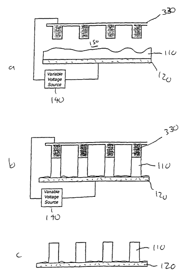
etchin;~. Such an embodiment 1S ShOWIl 111 Fig. 3a, where upper electrode 130
is replaced
with upper electrode 330, which is topographically patterned. In this case.
the externally
applied field causes the film undulations to focus in the direction of the
electric field
~,radient, i.e., in the direction of increasing electric fields. As a result,
the dielectric film
forms a pattern corresponding to the topographically patterned electrode 330,
as shown in
Fig. 3b. Upon solidifying the dielectric film, the columnar structure is
retained, as shown in
Fig. 3c. In addition, the aspect ratio of the patterned film can be
significantly ~~reater than
that of the patterned electrode. To increase the aspect ratio, the spacing
between the upper
electrode and the substrate is increased, while the film is liquilied and the
volta~~e is applied.
if necessary. the voltage can be varied during the relative displacement of
the electrode and
the substrate. Furthermore, in other embodiments, the lower electrode can also
be patterned.
either in the alternative, or in addition, to the upper electrode.
The embodiment ShOWIl 111 Figs. 3a-c provides one example of how one can
laterally
vary the strength of the electric field along interface 154 to define the
lateral structure. In
another example, the electric field strength along the interface can also be
made to vary
laterally by providing one or both electrodes with multiple, lateral regions
having different
conductivities. For example, the composition of one or both of the electrodes
can vary
laterally (e.g., separate lateral regions containing different metals).
Furthermore, one can
vary the electric field strength at the interface by introducing a layer
having a lateral variation
in dielectric material between the upper and lower electrodes. Finally, rather
than using a
single upper electrode and a single lower electrode, one can laterally vary
the electric field
strength by using multiple, independently addressible electrodes to generate
multiple volta~~e
7
CA 02395760 2002-06-21
WO 01/47003 PCT/US00/35139
differences across the interface between different pairs of the electrodes.
Embodiments of
the lnvellt1011 111ay include any one or any combination of such techniques to
laterally vary
the electric field strength along the interface and thereby provide a template
for the formation
of the lateral structure.
In a further embodiment, shown in Fig. 4a, substrate 120 is replaced with
substrate
420, which has a lateral variation in its surface energy. The lateral
variation in surface
energy can be produced, for example, by micro-contact printing, electron or
ion-beam
etching. and patterned deposition of any of, e.g., perfluorinated materials.
metals. and scli~-
assembled alkane thiols. Thereafter, film 110 is deposited onto substrate 420.
As in the
other embodiments, the film is liquified and a voltage is applied to the
electrodes. The
electric field results in an instability of the dielectric film, as described
above. The
developing surface undulations align with respect to the surface energy
pattern of the
substrate. This structure in the dielectric film is again preserved in the
absence of the electric
f eld by solidifying the polymer, as shown in Fig. 4b. Alternatively, in other
e117bOd1171e11tS.
1 Welectrode 130 and adjacent gap 160 can have a lateral variation in surface
ener~~y. rithcr in
the alternative, or in addition, to electrode 420. In further
eIllbOd1111eI1tS. it is also possible to
have a lateral variation in the surface energy of one or both of the
electrodes. and a
topographical pattern on one or both of the electrodes, and/or any other
combination of the
techniques described above for laterally varying the electric field strength
along the interface.
2p In any of the embodiments described above, the upper electrode can be
treated with a
release agent to facilitate its removal from the solidified, patterned film.
For example. usin'=
techniques 1110W11 111 the art, a self assembled alkalle monolayer can be
formed on the top
electrode prior to use to facilitate such removal.
Although not meant to limit the invention in any way, the following discussion
may
25 provide theoretical guidance for the above and additional embodiments of
the invention.
Theoretically, the origin of the film instability can be understood when
considering
the balance of forces, which act at the interface. The interfacial forces
(e.g., surface tension y)
minimize the interfacial surface area and stabilize the homogeneous film. The
electric field.
on the other hand, polarizes the film resulting in an effective displacement
charade density at
30 the liquid-air interface. which destabilizes the ,film. When written in
terms of pressures, the
electrostatic pressure p~i opposes the Laplace pressure. A local perturbation
in the film
thickness results in a pressure gradient that drives a flow of the film liquid
in the plane of the
8
CA 02395760 2002-06-21
WO 01/47003 PCT/US00/35139
film. The liquid flow next to a solid surface is given by a Poiseuille type
formula, which.
together with a mass conservation equation, establishes a differential
equation describing the
temporal response of the liquid. A common approach to investigate the effect
of external
forces on a liquid film is the linear stability analysis. A small sinusoidal
perturbation is
applied to an otherwise flat film and its response is calculated with the help
of a linearized
version of the differential equation. The resulting dispersion relation
quantifies the decay or
amplification of a given perturbation wavelength with time. The fastest
amplified mode is
given by:
~ "' - 2~c 2Y ( 1 )
ahel
a~
in which ~~", is the wavelength of the mode and corresponds to the resolution
of the formed
pattern, pn is a function of the electric field and the dielectric constant of
the film, and h is
the thickness of the film.
The dotted and dashed lines in Fig. 5 show ~.", as a fimction of the electric
field for
slightly different models of the electrostatic pressure peg. A similar
equation quantifies the
characteristic time z", for the formation of the instability (right hand axis
in Fi~.:. ~). The
experimental data shown in Fi~l. ~ will be described further below.
For the limit of a vacuum gap separating the upper electrode ti-om the film,
expressions for 7~", and z", can further be expressed as:
3
7~ = 2~ Y . ~ Ed - hJ 2 ~ 1 (
"' so s-1 U
_ 3rly 1 Ed - h 6 1 ( ;)
Tm - ~2 . y!3 CE-1 ~ . U9
0
where tile applied voltage between the electrodes is U, the surface energy of
the film is y , the
dielectric constant of the film is s , the film viscosity is r1 , and the
plate separation is d. In
9
CA 02395760 2002-06-21
WO 01/47003 PCT/US00/35139
general, the equations indicate th:~t no features are formed without the
presence of the
externally applied field. They al:.o indicate that the resolution of the
pattern is arbitrarily
small because, in principle, d, h, and 1 ~ can be arbitrarily controlled. For
example, non-
conductive spacers can be used to precisely control the electrode spacing. For
suitable
parameters, the electric field is typically in the range of about 10' V/m, and
the time required
to produce small features is sub-second. Furthermore, if desired, the surface
energy of the
film can be adjusted by introducing materials such as surfactants or block
copolymers, or
additives that increase or decrease the surface energy.
For the case of a liquid material separating the film from the upper
electrode, the
difference in dielectric constant across the interface decreases, which would
tend to increase
the value for 7~", . In practice, however, this is more than compensated by a
decrease in the
Laplace pressure for a liquid-liquid interface versus a liquid-air interface.
For wample. a
typical Laplace pressure for a liquid-air interface is about 30 dynes/cm2.
whereas the Laplace
pressure for a water-oil interface is about 1 dynes/cm'. This is explained
with further
reference to Fig. 6. The dependence of 7~", on the dielectric constant
difference between the
liquids, i.e. Ds = s, - ~Z, while keeping other variables constant, is shown
in Fig. 6 (dashed
line, left and top axis). ~,", diverges at the point where the dielectric
constants of the two
media are equal, i.e. Os = 0. This is understandable since the
polarizabilities of the liduids
are equal and the electric field does not exert any pressure on the
liquid/liquid interface. The
solid line (left and bottom axis) of Figure 3 illustrates a simple route to
achieve smaller sized
structures. These results show the scaling of ~,", as a function of the
interface or surface
tension. It is seen that 7~"I ~ y,, . As described above, a strategy to reduce
y,~ is by the
addition of a small amount of a dibloclc-copolymer that segregates to the
liquid/liquid
interface. Similarly one can achieve an effective reduction of the surface
tension ol~ a ainyle
2, layer by placing a surfactant or any additive that reduces yiz at the
liduid/air inmriacc. Om
consequence of the reduction in ~.",~". for the bilayer is a dramatic decrease
in time required to
alllpllty fILlCiLlat1O11S. Illtllltlvely, one would expect that the presence
of the SeCOlld vISCOLlS
medium would slow the growth of fluctuations substantially. On the contrary,
experimental
results (described in further detail in Example 3) show a 50-fold reduction in
this
characteristic time relative to a liquid-air structure.
CA 02395760 2002-06-21
WO 01/47003 PCT/US00/35139
While the topography of the film occurs spontaneously, control of the lateral
structure
is achieved by laterally varying the electric field strength at the interface
as described above.
For example. recall that the upper electrode can be replaced by a
topographically patterned
master. as described in reference to Fig. 2a-2c. Because the electrostatic
forces are strongest
for smallest electrode spacings d. the time for the instability to form is
much shorter for
smaller values of d (see Fig. 5, right hand axis). As a consequence, the
emerging structure in
the film is, focused towards the electrode structure. This leads to a
replication of the master
electrode.
In general, embodiments of the invention exploit the use of electrostatic
forces to act
on a dielectric boundary. If the inter-electrode spacing is chosen small
enou;~h ( < 1 ym).
small applied voltages ( ~ 30 V) are sufficient to generate high electric
fields (10~-10~ V/m)
in the dielectric tihn. This results in strong pressures that act on the
dielectric boundary
( ~ 10 I<N/mz). These forces cause the break-up of the dielectric film. For a
laterall5-
homogeneous electric field, the film instability features a characteristic
wavelength, which is
1 ~ a function of the electric field strength and the dielectric constant of
the film and is wel l
described by a linear stability analysis. if one of the electrodes is replaced
by a patterned
master. the electrode structure is replicated by the dielectric medium. As
described in the
experimental results below, lateral length scales down to 140 nm and aspect
ratios close to 1
have been created. The extension to lateral length scales of less than 100 nm
and aspect
ratios greater than 1 are possible.
The patterning methods disclosed herein can have many applications.
For example, the methods can be used in microlithographic applications where
the
patterned film is formed on the substrate as a mask to selectively expose some
regions ul~ tlm
substrate and not others. Once formed. the pattern can be transferred to the
substrate by
removing a layer of the substrate at each of the exposed regions, e.g., by
chemical or reactive
ion etching techniques. Alternatively, a layer of material can be deposited
onto the patterned
substrate to fill the exposed regions. For example, the exposed regions can be
tilled with
metal to provide wires within an integrated circuit.
Furthermore, using the techniques disclosed herein, multiple patterned tilms
can he
built up on a single substrate. For example. an additional layer can be
deposited over the lirst
patterned film to immobilize it during subsequent pattern formation above the
additional
layer. Moreover, in addition to being a mask for microlithographic
applications, the
11
CA 02395760 2002-06-21
WO 01/47003 PCT/US00/35139
patterned films may themselves provide functionality for any multilayer
structure formed
using the methods disclosed herein. For example, the patterned film can be a
patterned
semiconducting layer in an integrated circuit.
The patterning techniques disclosed herein are not limited to the fabrication
of
integrated circuits. They can also be used to form single or multiple
patterned surfaces as
pal-t of, e.g., a display device or a chemical, biological, medical, or
mechanical sensor.
Returning again to microlithography applications, the methods disclosed herein
IlICILIde lllally advantages over conventional photolithography techniques.
Ill SLICK
techniques, optical radiation passes tluough a mask or reticle to expose
selected regions of a
photoresist layer deposited on a substrate. Typically a wet chemical etch
follows to remove
either the exposed or unexposed regions of the photoresist and thereby produce
a patterned
film on the substrate. In contrast, the techniques disclosed herein do not
require a wet
chemical etch to form the patterned film, instead the externally applied
electric field causes
mass transfer of the film material to form the pattern. As result, prOb1e111S
C01711170111y
associated with wet etching, such as under exposure or undercutting due to
over exposure are
avoided.
Furthermore, the techniques disclosed herein do not require the optical
exposure tools
necessary in photolithography. Moreover, the resolution of the techniques are
not limited by
any optical diffraction or scattering constraints. To the contrary, a single
master electrode
having a topography with resolution better than the diffraction-limited
resolution of
photolithography tool can be produced by, e.g., electron beam etching, and
then, using the
techniques disclosed herein, the master electrode can be used multiple times
to reproduce the
hlgh-reSOhltloll pattern on as a film on each of multiple substrates.
Examples
The invention will now be illustrated by way of the following llolllllllltlllg
examples.
Example 1 - Homogeneous Field
A thin polymer film of polystyrene (PS) of thickness h was spin-coated from
solution
onto a highly polished silicon wafer serving as one of the electrodes.
Subsequently. another
silicon wafer was mounted as the opposing electrode at a distance d leaving a
thin air gap.
The assembly was then heated above the glass transition temperature of the
polymer (T~,) and
a small voltage U (20-50 V) was applied. To assure the air gap, the top
electrode had a small
12
CA 02395760 2002-06-21
WO 01/47003 PCT/US00/35139
step. Using a wedge geometry, a range of d values could be achieved, while
locally
maintaining a nearly parallel electrode configuration. Air gaps ranging from
10011111 to I 000
nm were achieved in this way. The voltage and the geometry of the capacitor
device
determine the electric field. The electrostatic driving force scales with the
difference of the
electric fields in the polymer film, E," and the air gap. E,, increases v~~ith
decreasing values of
c! and 111CI'eaSlllg polymer film thickness I7. The low applied voltage
combined w lth tile small
distance between the electrodes (d < I ym) leads to high electric fields E,, (
10' - 10' V/m).
The electric filed caused a small current to flow through the device ( 10-50
mA/cm'). At high
electric fields the current is caused by an ion conduction mechanism mediated
by small
I 0 impurity molecules in the polymer matrix. After exposing the heated film
to the applied
voltage for a time ranging from several minutes to a few hours, the polymer
was
subsequently immobilized by quenching below T~. the top electrode was
mechanically
removed, and then the morphology of the polymer film was investigated by
optical and
atomic force microscopy (AFM).
The results of the experiment are shown in Figs. 7a-7d, which are optical
micrographs
of polystyrene (PS) films that were exposed to an electric field. In Figs. 7a
and 7b, a 93 nm
thick PS film was annealed for 18 hours at 170°C with an applied
voltage U= 50 V. In Figs.
7c and 7d, the film thickness was increased to 193 nm. Depending on the
electric field
strength and the exposure time. either surface undulations (Fig. 7a) or a
columnar structure
where the liquid bridges the gap between the electrodes (Fig. 7b) were
observed. Because
the two electrodes were not perfectly parallel, the electric field also
exhibits a small lateral
variation.
Qualitatively, different degrees of ordering were observed. The ordering
phenomenon
originates from the repulsion of the equally charged undulation maxima and
minima. While
2~ the film morphology in Fig. 7b exhibits only imperfect order, more complete
hexagonal
packing was achieved in Fig. 7c. The main difference between the two images is
the initial
thickness h of the polymer film. With otherwise similar parameters, this
increased thickness
leads to a more dense lateral arrangement of the polymer columns and to an
increased
column-column repulsion. As a consequence, an improved hexagonal order was
observed in
Fig. 7c compared to Fig. 7b.
While nearest neighbor interactions lead to a hexagonal symmetry, second order
effects can be observed as well, as demonstrated for the nucleated instability
in Fi'~. 7d. The
13
CA 02395760 2002-06-21
WO 01/47003 PCT/US00/35139
locally higher value of h at the r ucleation point leads to a higher electric
field and an
increased driving force. This caused a depletion of the nearest-neighbor
undulations. The
next-nearest neighbors, on the other hand, were again amplified. They formed a
rosette on a
circle with a radius r = 2~, and a circumference of 2nr ~ 12 ~., where ~, is a
characteristic
wavelength. Beyond the circle of next-nearest neighbors, the instability
decays with
increasing distance. In the absence of nucleation effects, a similar argument
also explains the
hexagonal closest packing of the columns in Fig. 7c, where each maximum is
surrounded by
six neighbors, corresponding to a circle with radius ~, and circumference ~ 6
~..
Another observation concerns the well-defined lateral length scale. 'l~he
wavelm'~th ~
is a function of electric field E,,, which varies inversely with the electrode
spacing. 'l~he
lateral structure dimensions as well as the plateau height is readily measured
with the AEM
yielding ~. as a function of electrode spacing d. In Fig. 5, ~. is plotted as
a function of the
electric field E,, in the polymer layer. For a given film thickness h, the
characteristic lateral
structure size exhibits a power-law dependence as a function of the increasing
electric field,
corresponding to a decrease in the electrode spacing (top axis).
_Example ~ - Heterogeneous Fields
A patterned electrode was mounted facing a brominated polystyrene film (h ~ 4J
11111).
and the film was subjected to an applied voltage of 42 V. The device was
maintained at
170°C and exposed to the applied voltage for 20 hours. To ensure that
no polymer remained
on the master electrode after disassembly, the electrode was rendered unpolar
by depositing
of a self assembled monolayer. Fig. 8 is an AFM image that shows 140 nm wide
stripes
(full-width half maximum), which replicate the silicon master electrode (200
nm stripes
separated by 200 nm wide and 170 nm deep grooves). A cross-section measurement
reveals
a step height of 125 nm, with the resolution being limited by the geometry of
the AFM tip.
The profile of the polymer stripes is nearly rectangular with an aspect ratio
of 0.83. The high
quality of the replication extended over the entire 100 x 100 p.m2 area that
was covered by
the master pattern.
_Example 3 - Bilayer Liguids
Thlll liquid films of polyisoprene (PI) and oligomeric styrene (OS) were spin-
coated
from toluene solutions onto bare and gold-coated silicon wafers, respectively.
The film
14
CA 02395760 2002-06-21
WO 01/47003 PCT/L1S00/35139
thickness was 140 nm. For some experiments, a small air gap was left above the
liquid to
form liquid/air bilayers. In the remaining exper invents, the air was replaced
with a layer of
oligomeric dinvethylsiloxane (ODMS), thus forming a liquid/liquid bilayer. No
solvent was
used to deposit the ODMS layer. The overall thickness of the bilayer was
nominally 1 Vim.
Table 1 below summarizes the physical constants of the liquid oligomers and
polymers. From
the scientific literature, the interfacial tension of OS/ODMS, OS/PI and
PI/ODMS are 6.1
mN/m, 1.68 nvN/m and 3.2 111N/111, respectively. Thin rails of silicon oxide
were evaporated
on top of indium-tin-oxide (ITO)-coated microscope slides (Delta Techologies),
and these
slides were mounted on top of the bilayemsamples with the ITO and silicon
oxide side tacin~~
the bilayer samples. The separation distance between the substrate (Si wafer)
and the upper
boundary was thus controlled by the height of the evaporated spacers and was
typically
I .O8 X111. The samples were placed under an optical microscope and a small
voltage
(U = 20 V for PI/air, PI/ODMS bilayer experiments and U = ~0 V for OS/air_
OS/ODM~
l~ilayer experiments) was applied between the Si substrate (electrode 1 ) and
the Ifl'O laves
1 ~ (electrode 2). As the ITO-coated substrates do not significantly absorb
light in the visible
range, this geometry permitted a direct observation of the temporal evolution
of the thin
liquid films in the electric field.In the first set of experiments, a layer of
PI was placed
between the electrodes, leaving an air gap of 940 nm. An amplification of
fluctuations at the
PI/air interface, occurred, ultimately leading to the creation of an array of
vertically standing
PI columns. The average distance between the center of two neighboring columns
is
<~a,.r-a,n> = 47.44.4 Vim.
The influence of changes in a and y of the upper layer on the time and size
scales of
the evolving structures was investigated in the second set of experiments
involving a
PI/ODMS bilayer annealed at ambient conditions. Again a cylinder structure
results, but
there is a clear reduction in length scale, associated with the replacement of
air by ODMS.
The cylinder structures now exhibit a typical spacing of <d~yi_~yJ> = 20.61.3
Vim. This
spacing is about one-half that observed in the single film experiments. The
characteristic
times for the growth of the cylinders were determined for both the sin~~le and
bilayers cases
by optical microscopic observations. The time required to produce the first
observable
features was taken as the characteristic time. Notably, the time required to
produce the
cylindrical structures at the PI/ODMS interface was about one hour, nearly 50
times faster
than the time needed to produce the columns in the single film case.
Additional experiments
CA 02395760 2002-06-21
WO 01/47003 PCT/US00/35139
on OS/air and OS/ODMS bilayers showed essentially the same behavior, with
<d~,~,_~,.,> = 12.72.8 ~tm for OS/air and <d~,,~_~,,~> = 7.62.9 ~m of OS/ODMS.
Table 1
OS PI ODMS
y (mN/nl) 39 32 20
2.5 2.37 2.93
Mn 580 40,000 commercial grade
rl (Poise) 15 400 O.l
Other Embodiments
It is to be understood that while the invention has been described in
conjunction with
the detailed description thereof, that the foregoing description is intended
to illustrate and not
limit the scope of the invention, which is defined by the scope of the
appended claims. C>ther
aspects, advantages, and modifications are within the scope of the following
claims.
What is claimed is:
16