Note: Descriptions are shown in the official language in which they were submitted.
CA 02395797 2005-08-16
METHOD AND APPARATUS FOR THE CORRECTION OF OPTICAL SIGNAL
WAVE FRONT DISTORTION USING ADAPTIVE OPTICS
10
Field of the Invention
The present invention is related generally to the correction of distortion of
optical signals and, in particular, to the use of adaptive optics to correct
that
distortion.
IS
Background of the Invention
There are nearly limitless uses for optical signals in many different fields
for many different purposes. For example, such signals may be used in
communications systems when analog or digital data is modulated upon an
20 optical carrier signal, such as in an optical switch. Signals in such
systems are
then transmitted from one point to another using fiber optics or via free-
space
transmissions. Additionally, optical signals collected by telescopes are used
in
astronomy to view distant astronomical bodies and phenomena. There are also
many uses for optical signals in the medical field. For example, by
transmitting
-1-
CA 02395797 2002-07-26
Kurczynski 1 - 10
an optical signal into the human eye, it is possible to detect the light
reflected off
of the retina in that eye and then create an accurate map of the retina.
The operation of systems using optical signals may be hampered by a
variety of factors. For example, distortion of a transmitted planar wave front
of
s the light beam may occur due to any changes in the refractive properties of
the
medium through which the beam passes, including changes due to temperature
variations, turbulence, index of refraction variations or other phenomena.
This
distortion may cause discrete sections of the wave front to deviate from the
orthogonal orientation to the line of travel of the beam as initially
transmitted.
io This distortion may result in significant degradation of the wave front at
its
destination. In free-space communications systems, any disturbance in the
atmosphere between the transmission point and the receiving point may cause
certain portions of the beam to move faster than others resulting in the
aforementioned wave front distortion. The same is true in astronomical and
>s medical uses. For example, when used to create a map of the human retina,
wave front distortion does not typically result from atmospheric disturbance
but,
instead, results from the light beam passing first into, and then out of, the
eye
through its lens. The small imperfections on the fens and cornea distort the
wave
front of the beam much like the distortion seen in communications or
2o astronomical uses. Whatever the particular use, the result is the same:
distortion prevents a planar wave front of the beam from being received at its
destination in phase.
-2-
CA 02395797 2002-07-26
Kurczynski 1 -10
Adaptive optics uses a wave front sensor to measure phase aberrations in
an optical system and a deformable mirror or other wave front compensating
device to correct these aberrations. Deformable mirrors change their shape in
order to bring the reflected wave front into phase. Until recently, these
mirrors
were typically deformed via piezoelectric drivers, mechanical screws, or other
well-known methods. In recent methods, however, a deformable mirror may be
actuated. by a technique wherein an array of electrodes is located in
electrostatic
proximity to that mirror in the optical system. Electrostatic proximity means,
as
used herein, that by placing a voltage across these electrodes, an attractive
force
io is created between those electrodes and the mirror. This procedure is known
as
electrostatic actuation. By controlling the attractive force along different
portions
of the mirror surface, the shape of the mirror may be altered in a known way,
thereby at least partially correcting for the wave front distortion. Another
adaptive
optics method involves using magnetic forces to attract or repel portions of a
is mirror.
Systems using such deformable mirrors, however, have significant
limitations. For example, prior art adaptive optics systems relying on
electrostatic
actuation to correct the shape of a wave front cannot cause an attraction
between a particular electrode and a discrete portion of the mirror in one
instant,
2o and then cause a repelling electrostatic force between that particular
electrode
and that same portion of the mirror the next instant, or vice versa.
Additionally,
the voltage necessary to create a given pressure at a particular location on
the
mirror is nonlinearly dependent upon the distance from the mirror to the
relevant
-3-
CA 02395797 2002-07-26
KurczynskP 1 - 10
electrode. Since this distance is always changing (e.g., portions of the
mirror
would be drawn closer to the electrode when the mirror was actively deformed),
the same voltage used in different instances could cause significantly
different
results in the shape of the mirror at a particular location. Deformable
mirrors
using magnetic force to alter the shape of a mirror in order to correct the
shape of
the wave front also have significant limitations. For example, such mirrors
required electric coils that, when energized, created significant heat. This
heat
has the effect of rendering the mirrors unsuitable for certain uses (e.g.,
infrared
imaging) and, in extreme cases, could result in undesirable thermal stresses
to
io various components of the system.
Summary of the Invention:
The aforementioned problems related to wave front distortion correction
are solved by the present invention. In accordance with the present invention,
a
i5 bound charge is integrated within a mirror or in a material mechanically
coupled
with the mirror. A portion of the bound charge layer near a particular
electrode in
a first group of electrodes located in electrostatic proximity to the bound
charge
layer will aitemately be attracted or repelled from that particular electrode
by
changing the sign of the voltage across that electrode. Thus, the mirror that
is
2o mechanically coupled to this bound charge layer will similarly be attracted
or
repelled from that particular electrode. In one embodiment, a second group of
electrodes located on the opposite side of the mirror from the first group of
electrodes may be used to define the electrical field and enhance the ability
of a
-4-
CA 02395797 2002-07-26
Kurczynski 1 - 10
particular electrode in the first group to selectively attract or repel a
particular
portion of the mirror. It is advantageous to arrange the groups of electrodes
in
planes.
Brief Descrlntlon of the Drawincr
FIG. 1 shows a prior art mirror redirecting an incoming light beam in a new
direction;
FIG. 2 shows a prior art mirror wherein electrostatic force generated by a
plane of electrodes is used to alter the shape of the mirror;
io FlG. 3 shows a prior art mirror wherein a second plane of electrodes in the
optical path is used to increase the degree of deformation of the mirror;
FIG. 4 shows a mirror in accordance with one embodiment of the present
invention wherein a bound charge layer is affixed to the mirror;
FIG. 5 shows the mirror of FIG. 4 wherein a first plane of electrodes and a
is second plane of electrode, on opposite sides of the mirror respectively,
are used
to define the electrical field around the mirror; and
FIG. 6 shows a graph showing the relationship between spatial frequency
and amplitude of deformation of both prior art mirrors and the mirror in FIG.
4.
2o Detailed Description of the Invention
FIG. 1 shows a prior art structure utilizing a mirror 101 to reflect or focus
light beam 102. Light beam 102 may be an optical signal passing through an
optical network switch, an optical signal in a free-space optical
communications
system, light reflected from a portion of the human eye, or a light beam in
any
-5-
CA 02395797 2002-07-26
Kurczynski 1 - 10
other application whereby a mirror is used to focus or alter the path of the
beam.
The mirror 101 may be created by etching a silicon substrate with one side of
the
substrate deposited with one or more layers of material such as silicon
nitride,
single crystal silicon, polysilicon, polyimide, or other known materials,
using
methods that are well known in the art.
In order to create an easily-deformable mirror, the material is typically
etched, leaving side walls 103, until a membrane of as little as 1 micron
remains.
The membrane is reflective such that, upon reaching the mirror, tight beam 102
traveling in direction 104 is reflected from the surface of the mirror and is
>,o redirected in direction 105. A metallic coating (e.g., aluminum) may be
formed
on this membrane to enhance reflectivity. Tension is maintained in mirror 101
by
connecting side walls 103 to a supporting frame using well known methods.
As previously discussed, wave front distortion may result when any
changes to the refractive properties of the transmitting medium are
encountered
is along the line of travel 104 of the light beam. These changes may cause
discrete
sections of the wave front of the beam to deviate from their transmitted,
orthogonal orientation to the line of travel 104 of the beam 102. The result
is a
distortion of the image of the wave front when it reaches its destination,
which
may be for example a mirror, a focal plane of a telescope, an optical wave
front
2o sensor (e.g., a curvature wave front sensor or a Shack-Hartman wave front
sensor), or any other destination. By way of example, in optical
communications
systems, distortion may result in significant degradation of the
communications
signal or even the total loss of communications.
-6-
CA 02395797 2005-08-16
FIG. 2 shows the structure of FIG. 1 wherein electrostatic force is used to
deform the reflective surface of the mirror to correct for wave front
distortion of
the light beam 102 in accordance with the prior art. The mirror 201
illustrated in
FIG. 2 can at least partially correct for the effects of wave front
distortion. By
s measuring the aforementioned distortion using well-known techniques, the
shape
of the mirror necessary to correct for that distortion is determined. The
mirror
201, which is suspended between side walls 203 and is grounded, is deformed
using an electrostatic force that is created by passing a voltage across at
least
one electrode in a plane 202 of electrodes a distance d below the mirror 201.
By
io then selectively placing a voltage across one or more of those electrodes,
such
as electrode 204, located directly beneath the area of mirror 201 to be
deformed,
that area is attracted toward electrode 204 in direction 205. The result of
passing
various voltages across individual electrodes in plane 202 deforms the
different
sections of the mirror in a way such that, when the light beam is incident
upon
is the mirror 201, the aforementioned wave front deformation is reduced. The
aforementioned technique for correcting wave front distortion by detecting
said
distortion and translating that information into discrete voltages to create
deformation of a mirror is well known in the art.
CA 02395797 2002-07-26
Kurczynski 1 - 10
FIG. 3 shows the structure of FIG. 2 wherein the reflective surface of
mirror 301, which is suspended between side walls 303 and is grounded, can
compensate for a greater degree of wave front distortion than the embodiment
in
FIG. 2. As previously discussed, the side walls 303 are mounted to a support
s structure using well known methods. The greater degree of compensation
afforded by the embodiment in FIG. 3 is accomplished by adding a second
electrode plane 307 at a distance d~ from that mirror on the opposite side of
the
mirror 301 from the first plane 302 of electrodes. As plane 307 is in the
optical
path of the light beam, that plane may consist of a transparent electrode, a
io circular electrode ring, or any otherelectrode type that will not
significantly
obstruct the path of the beam. When voltage V~ is placed across electrode 307,
mirror 301 is drawn toward that electrode in direction 306. As in the
embodiment
shown in FIG. 2, by passing a voltage across electrode 304, the mirror will be
attracted toward that electrode in direction 305. Such a wider range of
is movement in either direction 305 or direction 306 facilitates correction of
a
greater degree of wave front distortion of the light beam 102.
Systems using the prior art mirror structures of FIG. 1, 2, and 3 have
significant limitations. These systems cannot cause an attraction between a
particular electrode and a discrete portion of the mirror in one instant, and
then
2o cause a repelling electrostatic force between that particular electrode and
that
same portion of the mirror the next instant, or vice versa. Additionally, the
voltage necessary to create a given pressure at a particular location on the
mirror
is nonlinearly dependent upon the distance from the mirror to the relevant
_8_
CA 02395797 2002-07-26
Kurczynski i - 10
electrode. Since this distance is always changing (e.g., portions of the
mirror
would be drawn closer to the electrode when the mirror was actively deformed),
the same voltage used in different instances could cause significantly
different
results in the shape of the mirror at a particular location.
FIG. 4 shows a structure in accordance with one embodiment of the
present invention wherein a bound charge layer of material 404 is affixed or
otherwise mechanically coupled to a surface of the mirror 401. A bound charge,
as used herein, is a permanent or semi-permanent electric polarization of a
dielectric material. Such a polarization can be created, for example, by
io implanting charges in a dielectric material. Additionally, a ferroelectric
layer may
be polarized or the dielectric material may be exposed to ionizing radiation.
Mechanical coupling with a mirror, as used herein, means that the bound-
charged layer is integrated with the mirror; or is in contact with the mirror
through
a layer or layers of intermediate material or through another structure or
is structures (e.g., one or more posts or springs connecting the bound charge
layer
to the mirror).
Mirror 401 of thickness B may be produced, as discussed previously, by
etching a substrate of thickness D of silicon with one side of the substrate
deposited with a layer of material such silicon nitride, single crystal
silicon,
2o polysilicon, polyimide, or other known materials using well-known methods.
Etching from surface 402 will result in side walls 403 of depth A (typically
on the
order of 5 millimeters) and reflective mirror surface 401. The material
forming the
side walls 403 may be retained in the operational mirror as such material adds
-9-
CA 02395797 2002-07-26
Kurczynski 1 - 10
rigidity to the mirror structure. Etching a substrate to create membrane
mirrors is
only intended to be representative in nature. Any other method for creating a
mirror capable of being deformed electrostatically may be used to implement
the
present invention.
A layer 404 of dielectric material of thickness C is affixed to the surface of
the etched substrate opposite from the etched surface. An illustrative
material
suitable for this purpose is Teflon~ (or another dielectric material) which
may be
spin-coated or deposited or grown onto the substrate to create a layer of
material
one or a few microns thick. Once this layer 404 is formed, a persistent bound
io charge may be implanted therein via a corona discharge in a plasma with a
DC
electric field, or via other well known methods. Using such a discharge, a
charge
is created within the layer 404 of Teflon~ of a density from 10'' to 10'9
C/cm2 that
is persistent for many years under a variety of conditions. While a charge in
Teflon~ created in the above manner creates an acceptable bound charge layer,
is other methods of mechanically coupling a bound charge layer to the mirror
are
also possible. For instance, the mirror itself may be constructed of a
material
suitable for holding a charge. Alternatively, a charge may be created semi-
permanently in the mirror by attaching a capacitor to it.
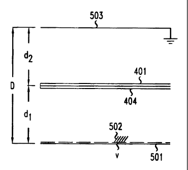
FIG. 5 shows an adaptive optics embodiment of the structure of FIG. 4. In
2o this embodiment, the mirror 401 is supported between two electrode planes,
501
and 503. Electrode plane 503 serves to add an electric field with known
characteristics above the bound charge layer. This field enables a greater
degree of control of the mirror 401. The two planes 501 and 503 are separated
-10.
CA 02395797 2002-07-26
Kurczynski 1 - 10
by distance D and may advantageously be placed at an equal distance from
bound charge layer 404 (i.e., d1 = d2). In operation, an optical signal is
received
by an optical system within which mirror 401 is supported. A well-known wave
front sensing technique (e.g., using a Shack-Hartman or a curvature wave front
sensor) is used to measure distortions in the wave front of the optical
signal. If
distortions are detected, well-known techniques are used to determine the
deformation of mirror 401 necessary to compensate for that distortion. As
previously discussed, placing a voltage across individual electrodes, such as
electrode 502 within plane 501, will result in a deformation of the mirror
401.
io Such electrodes may be arranged advantageously in an array in a way such
that,
by placing individually-controlled voltages across multiple electrodes in the
array,
multiple areas on the surface of the mirror 401 can be deformed to compensate
for the aforementioned wave front distortion. Since a bound charge is
implanted
into the dielectric material 402 mechanically coupled to the mirror 401, and
is because the electric field above the bound charge layer is known, changing
the
sign of the voltage passed over that electrode will result in a different,
known
direction of deformation. If the sign is the same as the sign of the bound
charge,
the area of bound charge layer 404, and hence mirror 401, nearest to the
respective electrode will be repelled away from that electrode. On the other
2o hand, if the sign of the voltage passed across the electrode is the
opposite of the
sign of the bound charge, the bound charge layer 404 and mirror 401 will be
attracted to that electrode. Electrode plane 503 is transparent and is in the
optical path of the light beam. This plane is a ground connection that,
together
-i i-
CA 02395797 2005-08-16
with electrode 502 and mirror 401 with dielectric material 402, serves to
define
the electric field geometry and adds predictability to the resulting
deformation of
the mirror 401 compared with the case where such a transparent electrode is
not
used. For the case where distance d2 in FIG. 5 is equal to distance d~, and
for
s small displacements of the bound charge layer 404, the pressure exerted on
the
bound charge layer 404 may be defined by the relationship:
P = Q V/ D (Equation 1 )
io wherein P is the pressure exerted upon the mirror, Q is the charge density
bound
within dielectric layer 402, and D is the distance between the two planes of
electrodes in FIG. 5. For the case where d2 is different from d1, this
equation
becomes:
is P = Q V/ D - QZ[(d2 - d1 )/(2EoD)] (Equation 1 a)
The pressure exerted on a prior art mirror such as used in FIG. 2 is
defined by the relationship:
2o P = 1/z(Eo V2/ d2) (Equation 2)
wherein P, once again, is the pressure exerted on the mirror, eo is a constant
(8.87 x 10-'2 F/m), V is the voltage passed over the relevant electrode, and d
is
the distance from the mirror to the plane of the relevant electrode. In the
case of
-12-
CA 02395797 2002-07-26
Kurczynski 1 - 10
the mirror as used in FIG. 3, wherein two planes of electrodes are used, the
pressure exerted upon the mirror potentially depends upon two different planes
of electrodes. In this case, the pressure is defined by the relationship:
P = ~heo {(V2/ d2) - (V~2/ d,2)} (Equation 3)
wherein P is the pressure upon the mirror at a particular location, Eo is a
constant, V is the voltage applied to an electrode 304 in FIG. 3 in plane 302,
d is
the distance from the mirror to electrode 304, Vi is the voltage applied to
electrode 308 in FIG. 3 within.plane 307, and di is the distance from the
mirror to
electrode 308.
io As is readily apparent from the equations, in accordance with the present
invention where d2 = d~ in FIG. 5, the pressure exerted on the bound charge
layer 404 in FIG. 5 defined by Equation 1 is entirely independent from the
distance of the mirror from any individual plane of electrodes. For any given
distance between planes 501 and 503 in FIG. 5, this pressure is directly
linear
with the voltage applied to the electrodes in plane 501. Controlling the
pressure
exerted upon the bound charge layer 404 is a matter of varying the voltage V
applied to the electrode 502. In the prior art cases described by Equations 2
and
3, the pressure exerted upon the mirror is dependent upon both the square of
the
voltage V and V~ and inversely upon the square of the distance from each plane
20 of electrodes, 302 and 307 respectively. As a result, the necessary voltage
V (or
V~) to achieve a unit increase in pressure P constantly changes with the
change
in the distances d and d~ from the mirror to the planes of electrodes.
Therefore,
-13-
CA 02395797 2002-07-26
Kurczynski 1 - 10
varying the pressure upon the mirror in these prior art cases requires a
complex
control algorithm.
FIG. 6 shows a graph of the amplitude of displacement of the mirror, 401
in FIG. 5, as a function of the spatial frequency of the membrane forming the
s mirror. Spatial frequency measures the degree of complexity of the mirror
shape
that the device may accommodate, and hence the complexity of wave front
distortion that the device can correct. Increasing the electrostatic pressure
(e.g.,
by increasing the voltage across an electrode) increases the spatial frequency
response of the membrane, represented by axis 601. Line 603 represents the
io relationship between spatial frequency and the amplitude of the
displacement of
the prior art mirror 301 in FIG. 3 used in conjunction with a single plane of
electrodes. Line 604 represents the same relationship for the embodiment of
the
present invention shown herein in FIG. 5 where a bound charge layer is used in
conjunction with two planes of electrodes. Both line 603 and 604 vary
inversely
is with the square of the spatial frequency, i.e. the amplitude of
displacement of the
membrane decreases as spatial frequency increases. However, for a given
spatial frequency 605, the prior art membrane of FIG. 3 will only exhibit
displacement amplitude 605, while the mirror used in the embodiment of the
present invention will exhibit a significantly higher displacement amplitude
606.
2o As a result, when using the mirror in accordance with the principles of the
present invention, less voltage is required to achieve the same displacement
as
in the prior art.
-14-
CA 02395797 2006-02-09
Further embodiments of the invention provide for an apparatus that
includes a plurality of mirrors. Each mirror being mechanically coupled to a
corresponding plurality of bound charge layers. This type of apparatus can
form the basis of an optical networking switch.
The foregoing merely illustrates the principles of the invention. It will
thus be appreciated that those skilled in the art will be able to devise
various arrangements that, although not explicitly described or shown
herein, embody the principles of the invention and are within its spirit and
io scope. Furthermore, all examples and conditional language recited herein
are intended expressly to be only for pedagogical purposes to aid the
reader in understanding the principles of the invention and are to be
construed as being without limitation to such specifically recited examples
and conditions. Diagrams herein represent conceptual views of mirrors
is and light beams. Diagrams of optical components are not necessarily
shown to scale but are, instead, merely representative of possible physical
arrangements of such components.
-15-