Note: Descriptions are shown in the official language in which they were submitted.
CA 02395868 2006-07-10
WO 01/58348 PCT/US01/04270
Title:
IlVIPROVED ANALYTE SENSOR AND METHOD OF MAK]NG THE
SAME
10
Field of the Invention
The present invention relates to methods for producing sensors that
include flexible substrates and one or more sensor electrodes, and in
particular
embodiments to sensor sets including such sensors.
Background of the Invention
Methods for producing sensors, particularly sensors useful in sensor sets
for the determination of a body characteristic such as blood glucose levels,
are
known. Exainples of such sensors, sensor sets and methods for production
thereof are described, e.g., in commonly assigned U.S. Patent No. 5,390,691;
No.
5,391,250; No. 5,482,473; No. 5,299,571; No. 5,586,553; and No. 5,568,8060
Certain lmown methods, such as that described in U.S. Patent No. 5,391,
250, form the sensor electrodes by an etching process. Etching processes are
often multi-step procedures that can be time-consuming and expensive.
Accordingly, a need exists for a simplified process for producing sensors.
.Alternative methods can be used to
form sensor
electrodes by, for example, first forming a channel in a substrate, which can
be a
continuous web, and then depositing conductive material in the cliannel to
form
the electrode.
-1-
CA 02395868 2002-06-21
WO 01/58348 PCT/US01/04270
A need also exists for an improved process that enables continuous
formation of sensors.
Summary of the Preferred Embodiments
It is an object of an embodiment of the present invention to provide an
improved sensor and method of making the same, which obviates for practical
purposes, the above mentioned limitations.
According to an embodiment of the invention, a sensor and a method of
making the same for implantation in a body includes a substrate with notches
cut
in the substrate to foim a necked down region in the substrate; and at least
one
sensor electrode formed from one or more conductive layers. In preferred
embodiments, the thickness of the substrate ranges from approximately 25 to
350 , but the thickness of the substrate can range from 5 to 750 . In
particular
embodiments, a sensor assembly includes the sensor and a slotted needle having
a
slot. The notches creating the necked down region allow the substrate to slide
into the slotted needle, which that has the slot narrow enough to permit
passage of
the necked down region. However, a non-necked down region of the substrate is
prevented from pulling out of the slotted needle through the slot. In other
embodiments, the slot of the slotted needle permits the necked down region of
the
substrate to slide down the slot.
In further embodiments, a width of the substrate in the non-necked down
portion is sized to fit within a slotted needle having a diameter smaller than
21
gauge, 22 gauge, 23 gauge, 24 gauge or the like. In additional embodiments, at
least one of the at least one sensor electrode is foimed on a first surface of
the
substrate. In alternative embodiments, all of the at least one sensor
electrode are
only formed on the first surface. In other alternative embodiments, at least
another one of the at least one sensor electrodes is formed on a second
surface of
the substrate. In still other alternative embodiments, a third one of the at
least one
sensor electrode is a reference electrode configured to contact a skin
surface.
In yet another embodiment, sensors are formed as a part of sensor set that
includes a sensor, mounting base and insertion needle. The mounting base
adapted for mounting onto a patient's skin. The insertion needle is carried by
the
-2-
CA 02395868 2002-06-21
WO 01/58348 PCT/US01/04270
mounting base to protrude from the mounting base and has at least a portion of
the sensor nested within the insertion needle. The insertion needle defines a
longitudinally extending slot along one side to permit sliding withdrawal of
the
insertion needle from the mounting base and the nested portion of the sensor.
The slot is also configured to accept the necked down region of the substrate.
In accordance with one aspect of the present invention, there is provided a
method of making a sensor that includes the steps of providing a pre' formed
self-
supporting flexible substrate; sputter-depositing a metal layer on the
substrate;
etching the sputter-deposited metal layers to form a sensor electrode having a
proximal segment and a distal segment; plating a metal layer on the sensor
electrode; and separating the sensor electrode and at least a portion of the
substrate underlying the sensor electrode from the remainder of the substrate.
Preferably, the substrate is comprised of a polymeric material, such as a
polyimide, and in more particular embodiments, the substrate is supplied in
the
form of a continuous web.
In particular embodiments, a plurality of metal layers are sequentially
sputter-deposited, and the plated layer is formed on the uppermost sputter-
deposited layer of the sensor electrode. Preferably, the sputter-deposited
metal
layers are comprised of different metals, such as layers of chromium and
copper.
According to another preferred embodiment, prior to the sputter-
deposition step a layer of a material that promotes adhesion between the
sputter-
deposited metal layer and the substrate is deposited on the substrate. In
other
embodiments, during the plating step, a layer of copper or a layer of gold is
plated
on the sensor electrode. Alternatively, a plurality of layers are sequentially
plated on the sensor electrode.
In other einbodiments, prior to the separation step, the sensor electrode is
provided with a coating, such as a coating of a polymeric material, and/or a
biocompatible polymeric material. Preferably, the coating is subsequently
removed from the proximal segment and the distal segment of the sensor
electrode. In further embodiments, the coating is removed from the distal
segment of the sensor electrode and the distal segment is subsequently
provided
with an electrode chemistry. In other einbodiments, the sensor electrode is
-3-
CA 02395868 2002-06-21
WO 01/58348 PCT/US01/04270
provided witli a membrane after the distal segment is provided with the
electrode
cheinistry.
According to a particular embodiments, a plurality of sprocket holes are
formed in the substrate adjacent to the sensor electrode. Also, in preferred
embodiments, the step of removing the sensor is carried out using a laser.
In preferred embodiments, the substrate has an upper surface and a lower
surface. The sensor electrode is formed on the upper surface, and after the
etching step a bead is formed on at least one of the lower surface and the
sensor
electrode. The bead is formed, according to one particular embodiment, below
and in alignment with the sensor electrode. According to another particular
embodiment, a first bead is formed on the lower surface of the substrate and a
second bead is formed on the sensor electrode. Preferably, the bead is formed
using a liquid polymer, and is formed using a molding process.
In accordance with another embodiment of the present invention, a
method of malcing a sensor includes the steps of providing a pre-formed self-
supporting flexible substrate; sequentially sputter-depositing a plurality of
metal
layers on the substrate, the plurality of layers including an uppermost layer;
plating a metal layer on the uppermost sputter-deposited metal layer; etching
the
plated and sputter-deposited metal layers to form a sensor electrode having a
proximal segment and a distal' segment; sequentially plating first and second
metal layers on the sensor electrode; coating the sensor electrode with a
polymeric material; fonning at least one opening in the coating; and
separating
the sensor electrode and at least a portion of the substrate underlying the
sensor
electrode from the remainder of the substrate.
In preferred embodiments, layers of chromium and copper are sequentially
sputter-deposited. Preferably, at least one layer of copper is plated on the
sputtered layer(s) prior to etching, and layers of copper and gold are
sequentially
plated after the etching step.
In accordance with an additional embodiment of the present invention, a
method of making a sensor includes the steps of providing a pre-formed self-
supporting flexible substrate; sputter-depositing at least one metal layer on
the
substrate; etching the at least one metal layer to form a sensor electrode
having a
-4-
CA 02395868 2002-06-21
WO 01/58348 PCT/US01/04270
proximal segment and a distal segment; and separating the sensor electrode and
at
least a portion of the substrate underlying the sensor electrode from the
remainder
of the substrate.
In accordance with still another einbodiment of the present invention, a
method of making a sensor includes the steps of providing a substrate having
an
upper surface and a lower surface; sputter-depositing at least one metal layer
on at
least one surface of the substrate; etching the at least one metal layer to
fonn a
sensor electrode having first and second edges, a proximal segment and a
distal
segment; forming a bead on at least one of the upper surface and the lower
surface of the substrate; and separating the sensor electrode and the portion
of the
substrate underlying the sensor electrode from the remainder of the substrate.
In preferred embodiments, the sensor electrode is formed on one of the
upper and lower surfaces of the substrate and the bead is formed on the other
surface of the substrate. In a further embodiments, the bead is formed on the
substrate beneatli the sensor electrode.
According to particular embodiments, the bead is formed by forming a
perforation in the substrate adjacent to the first and second edges of the
sensor
electrode; securing the lower surface of the substrate to a mold, the mold
having a
channel that extends beneath the sensor electrode; flowing a liquid polymer
over
the upper surface of the substrate and tlirough the perforations into the
channel
until the polymer beads on the upper surface of the substrate and covers at
least a
portion of the sensor electrode; curing the liquid polymer; and removing the
substrate from the mold. In further embodiments, the perforations on each side
of
the sensor electrode include at least one perforation gap. The liquid polymer
that
flows over the sensor electrode does not cover the portion of the sensor
electrode
between the perforation gaps. The perforations on each side of the sensor
electrode may include a plurality of perforation gaps. In still other
embodiments,
each perforation has a perforation gap adjacent to at least one of the
proximal and
distal segments of the sensor electrode. In a preferred embodiment, the distal
segment is provided with an electrode chemistry.
According to yet another embodiment of the present invention, a method
of making a sensor includes the steps of: providing a substrate having an
upper
-5-
CA 02395868 2002-06-21
WO 01/58348 PCT/US01/04270
surface and a lower surface; forming at least one channel in at least one of
the
upper and lower surfaces of the substrate; disposing a conductive material in
the
at least one channel to form at least one electrode; and forming a bead on at
least
one of the upper and lower surfaces of the substrate to produce a sensor.
According to a further embodiment of the present invention, a method of
inalcing a sensor includes the steps of: providing a substrate having an upper
surface and a lower surface; disposing a conduetive material on at least one
of the
upper and lower surfaces of the substrate by non-impact printing to form at
least
one electrode; and forming a bead on at least one of the upper and lower
surfaces
of the substrate to produce a sensor.
According to yet a further embodiment of the present invention, a method
of making a sensor includes the steps of providing a substrate having an upper
surface and a lower surface; providing a film or sheet comprising a conductive
material; transferring the conductive material from the film or sheet to the
substrate to form at least one electrode; and forming a bead on at least one
of the
upper and lower surfaces of the substrate to produce a sensor.
According to still a further embodiment of the present invention, a method
of making a sensor includes the steps of: providing a substrate having an
upper
surface and a lower surface; depositing at least one layer of a metal on the
upper
surface of the flexible substrate; etching the at least one metal layer to
form a
sensor electrode having first and second edges, a proximal segment and a
distal
segment; forming a perforation in the substrate adjacent to the first and
second
edges of the sensor electrode; securing the lower surface of the substrate to
a
mold, the mold having a channel that extends below the metal layer; flowing a
liquid polymer over the upper surface of the substrate and through the
perforations into the channel until the polymer covers the upper surface of
the
substrate and at least a portion of the sensor electrode; curing the liquid
polymer;
removing the substrate froin the mold; and removing the sensor electrode, the
cured polymer and the portion of the substrate between the first and second
perforations by separating the substrate adjacent to the perforations.
According to another embodiment of the present invention, a method of
making a sensor includes the steps of: providing a substrate; forming a bead
on a
-6-
CA 02395868 2002-06-21
WO 01/58348 PCT/US01/04270
surface of the substrate; forming a sensor electrode on the substrate; and
separating the bead, the sensor electrode and at least a portion of the
substrate
between the bead and the sensor electrode from the remainder of the substrate.
According to yet another embodiment of the present invention, a method
of making a sensor includes the steps of: providing a substrate; forming a
sensor
electrode on a surface of the substrate; forming a bead on the substrate; and
separating the bead, the sensor electrode and at least a portion of the
substrate
between the bead and the sensor electrode from the remainder of the substrate.
In accordance with further embodiments of the present invention, sensors
produced according to the foregoing methods are also provided. In accordance
with other embodiments of the present invention, sensor sets that include
sensors,
as described herein, together with appropriate mounting bases and insertion
needles are provided. In additional embodiments, the sensor sets include
cannula
in which portions of the sensor are disposed and wliich in tuxn are at least
partially disposed within the insertion needles. In other embodiments, the
sensor
includes a bead, which is at least partially nested within the insertion
needle,
obviating the need for a cannula.
Other objects, features and advantages of the present invention will
become apparent to those skilled in the art from the following detailed
description. It is to be understood, however, that the detailed description
and
specific examples, while indicating preferred embodiments of the present
invention, are given by way of illustration and not limitation. Many changes
and
modifications within the scope of the present invention may be made without
departing from the spirit thereof, and the invention includes all such
modifications.
Brief Description of the Drawings
A detailed description of embodiments of the invention will be made with
reference to the accoinpanying drawings, wherein like numerals designate
corresponding parts in the several figures.
FIGS. 1-4 illustrate an embodiment of a first method according to the
invention in which a substrate, illustrated as a flexible tape supplied from a
reel,
-7-
CA 02395868 2002-06-21
WO 01/58348 PCT/US01/04270
is provided with at least one metal layer deposited on its upper surface, an
optional plating of one or more metal layers, followed by an etching step to
form
one or more sensor electrodes, and an optional plating of one or more
additional
layers, after which the metal layer(s) and the underlying portion of the
substrate
are subsequently separated from the remainder of the substrate;
FIG. 1 is an illustration of a reel and tape used to provide a substrate for
use in the methods in accordance with einbodiinents of the present invention;
FIG. 2a is a cross-sectional view of the substrate as viewed along the line
2-2 in FIG. 1 with the inclusion of a sputter deposited layer.
FIG. 2b is a cross-sectional view of the substrate with multiple sputter
deposited layers;
FIG. 2c is a cross-sectional view of the substrate with multiple sputter
deposited and plated layers;
FIG. 2d is a cross-sectional view of the sensor electrode after it has been
etched baclc and the substrate after it has been formed with sprocket holes;
FIG. 2e is a cross-sectional view of a sensor electrode after additional
layers have been plated onto the sensor electrode;
FIG. 3a is a cross-sectional view of the substrate and sensor electrode after
being covered by a polymer coating;
FIG. 3b is a cross-sectional view of the substrate and sensor electrode
after the polymer coating has been etched back;
FIG. 4 is a cross-sectional view of the sensor after being separated from
the remainder of the substrate;
FIG. 5 is a perspective view illustrating a sensor set that includes a sensor
formed according to the invention;
FIG. 6 is an enlarged longitudinal vertical section taken generally on the
line 6-6 of FIG. 5;
FIG. 7 is an enlarged longitudinal sectional of a slotted insertion needle
used in the insertion set of FIGS. 5 and 6;
FIG. 8 is an enlarged transverse section taken generally on the line 8-8 of
FIG. 7;
-8-
CA 02395868 2002-06-21
WO 01/58348 PCT/US01/04270
FIG. 9 is an enlarged transverse section taken generally on the line 9-9 of
FIGS. 7;
FIG. 10 is an enlarged fragmented sectional view corresponding generally
with the encircled region 10 of FIG. 6;
FIG. 11 is an enlarged transverse section taken generally on the line 11-11
of FIG. 6;
FIGS. 12a-b are transverse sections of alternative embodiments of a
sensor produced according to the invention that include tubular (FIG. 12a) or
solid (FIG. 12b) beads;
FIG. 13 is a transverse section illustrating the engagement of the sensor of
FIG. 12a and a slotted insertion needle;
FIG. 14 is a transverse section illustrating another alternative embodiment
of a sensor of the invention including beads on each side of the sensor, and
the
engagement of the sensor with a slotted insertion needle;
FIGS. 15-21 illustrate another alternative embodiment of a method
according to the invention, wherein
FIGS. 15a-b are side sectional views illustrating deposition of a metal
layer (FIG. 15a) or metal layers (FIG. 15b) on a flexible substrate,
FIG. 16 is a transverse section illustrating formation of perforations on
either side of the metal layer of FIG. 15a,
FIG. 17 is a transverse section showing the position of the substrate of
FIG. 16 in relation to a mold having defined therein a channel;
FIGS. 18a-b illustrate provision of a liquid polymer through the
perforations formed in the substrate into the mold chamiel (FIG. 18a) and its
beading over the upper surface of the substrate and the metal layer (FIG.
18b);
FIG. 19 is a transverse section illustrating the curing of the liquid
polymer;
FIG. 20 is a side section illustrating disengagement of the mold from the
substrate and the cured polymer;
FIG. 21 is a transverse section along the lines 21-21 of FIG. 20 showing
separation of the completed sensor from the remainder of the substrate;
-9-
CA 02395868 2002-06-21
WO 01/58348 PCT/US01/04270
FIG. 22 is a sectional view of an alternative embodiment of the inventive
method in which a sensor membrane is provided after the liquid polymer is
supplied;
FIGS. 23-25 illustrate alternative methods for producing sensors, after
which beads are provided in accordance with the methods described herein, in
which
FIGS. 23a-b illustrate a first alternative method in which channels are
formed in a substrate and subsequently filled with a conductive material to
form
the sensor electrodes,
FIG. 24 illustrate a second alternative method in which sensor electrodes
are formed electrographically using a conductive toner, and
FIGS. 25a-b illustrate a third alternative method in wliich sensors are
formed by a printing process;
FIG. 26 is a top plan view of a sensor in accordance with another
embodiment of the present invention;
FIG. 27 is a side plan view of the sensor shown in FIG. 26; and
FIG. 28 is a partial cross-sectional view of the sensor of FIG. 26 inside of
an insertion needle.
Fig. 29 is a top plan view of another sensor similar to the embodiment of
the sensor shown in Fig. 26.
Figs. 30(a) and (b) are plan views of an alternative embodiment of the
sensor shown in Figs. 26-29.
Figs. 31(a) and (b) are plan views of another alternative embodiment of
the sensor shown in Figs. 26-29.
Detailed Description of the Preferred Embodiments
As shown in the drawings for purposes of illustration, the invention is
embodied in an improved sensor and method of manufacturing the sensor. In
preferred embodiments of the present invention, the sensor is a glucose sensor
that utilizes glucose oxidase. However, alternative einbodiments may use other
materials, such as optical, fluorescence or electrical materials to sense the
glucose
levels, or may uses other materials to sense the presence of different
analytes,
-10-
CA 02395868 2006-07-10
WO 01/58348 PCT/US01/04270
such as, including but not limited to, HN, viruses, medication levels,
cholesterol,
hormones, fluids or the like. Preferred embodiments are for use with humans.
However, it will be recognized that further embodiments of the invention may
be
used in animals, laboratory tests, agriculture related testing, or the like.
According to embodiments of the inventive method, sensors are produced
by deposition of a metal layer or layers followed by etching production
methods.
Subsequent layers are then added by electroplating. The metal layer(s) can be
deposited on either a non-self supporting substrate, or in a preferred
embodiment
on a self-supporting substrate such as a polyimide tape. Thus, sensors can be
produced cleanly and at high density on the substrate according to the
inventive
method; and in further embodiments, the sensors can be produced on one or both
sides of the substrate.
Referring now to FIGS. 1-4, a substrate 10 is provided in accordance witli
a first embodiment of the inventive method. In preferred embodiments,
substrate
10 is a flexible, self-supporting substrate in the form of a continuous tape
12
supplied from a ree114. The continuous tape 12 is preferably formed from a
polymeric material such as a polyimide. However, other flexible, self-
supporting
materials can be used. The thickness of tape 12 is preferably about 101i to
125 .
However, in alternative embodiments, thinner or thicker films from 5 to 500
may be used. In particular embodiments, sprocket holes 15 (see Fig. 2c) are
formed in the substrate adjacent the outer edge of the tape 12 to facilitate
manufacturing of the sensors through automated processes. For, instance, the
tape
12 is fed through stages that perform various steps of the methods described
in
this application. Sensor electrodes 20 can be formed on the tape 12 using
techniques described in "3M Specifications and Design Guidelines, Microflex
circuits for IC Interconnect Solutions," pages 1-32 (the entire document),
1997
(3M Electronic Products Division, Austin TX), "3M Offers More Solutions for
the Semiconductor Industry" the entire document,1997 (3M Electronic Products
Division, Austin TX), and "Microflex Solutions from 3M", the entire document,
1996 (3M Electronic Products Division, Austin TX), all of which are publicly
available from 3M.
-11-
CA 02395868 2006-07-10
WO 01/58348 PCT/USOl/04270
Alternatively, substrate 10 can be formed by a casting process, for
example by spin-coating a layer of a liquid polyimide or other polymeric
material
onto a temporary glass carrier and then cured. Such substrates can be self-
supporting or non-self supporting. The sensor electrodes 20 can be formed on
the
substrate 10 using techniques described in "Micron Wide Conductors and Spaces
on ... PZT, Alumina, Glass and Flexible Materials" 1 page, no date
(Metrigraphics, Wilmington, MA), "Flexibel circuits at Extreme Density, 8
unnumbered pages of various dates (Metrigraphics, Wihnington, MA), and
"Metrigraphics Ion Beam Etching Capability", 1 page, no date (Metrigraphics,
Wihnington, MA), and all of which are publicly available.
Substrate 10 has an upper surface 16 and a lower surface 18. The
substrate 10 is preferably cleaned, and subsequently at least one metal layer
20a is
formed on the upper surface 16 of the substrate 10 by a deposition process
(see
FIG. 2a). A particularly preferred process is sputter deposition, or
sputtering.
Sputtering can be carried out using conunercially available sputtering
reactors
using an RF (radio frequency). Magnetron sputtering can also be carried out;
magnetron sputtering uses a magnetic field to concentrate electrons near the
target
surface to increase the deposition rate. Other known deposition processes,
such
as chemical vapor deposition (CVD) methods, can also be employed. The
thickness of the deposited layer preferably ranges from about 0.05 to about
300.0 , more preferably about 0.5 to about 25.O . When multiple layers are
deposited, the total thickness of the layers preferably has a thickness within
the
foregoing ranges.
One or more metal layers can be deposited on the substrate 10 according
to the inventive method. For example, two layers 20a and 20b of different
metals
can be deposited (see FIG. 2b). Exemplary metals include, but without
limitation,
elemental metals such as chromium, gold, copper, aluminum, nickel, tantalum
and titanium, alloys such as Inconel and Nichrome, and mixtures thereof. The
term "metal layer" is also intended to encompass layers that include one or
more
non-metallic elements in a mixture or chemical combination with one or more
metallic elements, and thus also encompasses materials such as oxides, for
-12-
CA 02395868 2006-07-10
WO 01/58348 PCT/USOI/04270
example alumina. Reactive as well as non-reactive layers can be formed;
reactive
materials, such as tantalum oxide, chromium oxide, etc., are also intended to
be
encompassed by the term "metal layer." Specific combinations of metal layers
that are useful according to the invention include chromium and copper; copper
and gold; and chromium, gold and chromium; copper, nickel and gold; and
chromium, copper, nickel and gold.
In particular embodiments, chromium forms the first sputtered metal
layer. Chromium provides an additional benefit in promoting adhesion between
certain polymeric materials, such as polyimides, and other metals. Other metal
layers, such as nickel or the like, that promote adhesion can also be employed
if
desired.
As shown in FIG 2d, in particular embodiments, subsequent to the sputter
deposition step but prior to an etching step, one or more metal layers 20c can
be
plated on the upper surface of the sputter deposited metal layer (or the
uppermost
sputter deposited layer if more than one such layer is prepared). Such layers,
in
preferred embodiments, are comprised of copper. However, in alternative
embodiments, other metals, such as nickel, chromium; gold, or the like, may be
plated onto the layers used to form the sensor electrodes.
After the sputter deposition of the metal layer(s), and/or one or more
layers are applied by plating, an etching process is carried out in order to
form the
sensor electrode 20 (see FIG. 2d). Any conventional etching process can be
employed. For example, the etching processes described above and in U.S.
Patent No. 5,391,250 issued February 21, 1995 to Cheney, II et al. and
entitled
"Method of Fabricating Thin Film Sensors"
may be used to form one or more sensor electrodes. In
alternative embodiments, the one or more metal layers applied by plating prior
to
etching may be omitted and just the sputtered layers are etched. Preferred
embodiments form the sprocket holes 15 by etching at the same time that metal
etching process is carried out. Alternative embodiments may form the sprocket
holes 15 before or after the etching of the metal layer(s). Sprocket holes 15
may
be formed by other methods, such as water knife, laser ablation, punching,
cutting, or the like.
-13-
CA 02395868 2002-06-21
WO 01/58348 PCT/US01/04270
In further embodiments, subsequent to the etching step one or more
additional metal layers 23 a, 23b can be plated on the sensor electrode(s) 20'
(see
Fig. 2e). The optional additional plating step is advantageous in providing a
protective coating over the sputter-deposited metal layers, including the
sides
thereof. In particular embodiments, layers of copper; copper and gold; or
copper,
nickel and gold are plated after the etching step. In preferred embodiinents,
gold
is plated over the sensor electrodes 20' as the final layer 23b to seal in all
of the
other layers.
As shown in FIG. 3a, in a preferred embodiment, prior to separation from
the remainder of the substrate, the sensor can be provided with a polymeric
coating 26, preferably formed from a non-toxic, biocompatible polymer. For
instance, the polymer coating 26 provides an insulative and/or protective
coating
that covers the substrate 10 and the sensor electrodes 20. Exemplary useful
polymers include, without limitation, polyimide, biocompatible soldermasks,
epoxy acrylate copolymers, or the like. In preferred embodiinents, the
polymers
are photo-iniaginable to permit portions of the polymers to be removed for
exposure of contacts, electrodes for application of sensor chemistry, or the
like.
Portions of the coating polymer are masked to form a pattern, which is them
exposed and developed to remove the portions of the polymer coating 26 for
further processing of the sensor 8. In alternative embodiments, the coating
polymer may be removed by other methods, such as by laser ablation, chemical
milling, or the like. Use of a secondary photo resist can be employed to
target
specific sites for removal. As shown in FIG. 3b, the coating polymer 26 is
etched
(ablated, milled, or the like) back to expose windows (or openings) 28 to
expose
the contact pads to pemiit connection with a monitoring device (discussed
below)
and to form windows (or openings) 28 over the sensor electrodes 20 to allow
sensor chemistry materials to be applied to the exposed sensor electrodes 20
to
complete the manufacture of the sensors 8.
In further embodiments, the exposed areas that form windows (or
openings 28) are plated with additional layers of metal. This saves money and
can reduce the thickness of the sensor electrodes, except where the thickness
or
layer is required. Plating after forming the windows (or openings) 28 also
allows
-14-
CA 02395868 2006-07-10
WO 01/58348 PCT/US01/04270
the plating to fill in any potential leaks around the windows (or openings) 28
caused by gaps between the polymer layer and the sensor electrodes.
Additionally, if the final metal layer is plated after the last etching and
coating
step, the surface of the final metal layer is in its best condition for
application of
enzymes and membranes. Thus, doing a final plating step increase reliability
and
predictability of sensor performance. In preferred embodiments, the fmal metal
layer is gold. However, in alternative embodiments, other final metal layers,
such
as platinum, iridium, chromium, copper or the like may be used.
After completion of the etching and optional plating steps and any
polymer coating steps, the sensor 8, including a portion of the substrate
underlying the metal layer(s) 23n forming the sensor electrode 20 and any
polymer coating 26, is removed from the remainder of the substrate (see FIG.
4).
In a preferred embodiment, the sensor is removed from the remainder portions
22
of the substrate 10 by cutting along lines 24, for example using a laser.
Other
known cutting devices, such as blades, ultrasonic, water knifes, or the like,
can
also be used.
Sensors formed according to the inventive method are usefully employed
in a variety of known sensor sets. Exemplary sensor sets are illustrated in
FIGS.
5-11, generally similar to those described herein, not including a bead, into
a
sensor set generally similar to that described in U.S. Patent No. 5,586,533,
to
Halili et al., and entitled "Transcutaneous Sensor Insertion Set", and U.S.
Patent
No. 5,954,643 issued September 21, 1999 to Van Antwerp et al. and entitled
"Insertion Set for a Transcutaneous Sensor".
In an embodiment illustrated in FIGS. 5-10, a sensor set
referred to generally by the reference numera1110 is provided for
transcutaneous
placement of a flexible sensor 112 (see FIG. 6) at a selected site within the
body
of a patient. The insertion set 110 includes a rigid hollow slotted insertion
needle
114 for quick and easy placement at a desired placement site (e.g.,
transcutaneous, intraperitoneal, peritoneal, etc.) of a cannula 115 with a
distal
segment 116 of the sensor 112 therein. The distal segment 116 has at least one
sensor electrode 118 (three are illustrated, which generally correspond to the
sensor electrode 20 described above), formed by deposition as described above,
-15-
CA 02395868 2002-06-21
WO 01/58348 PCT/US01/04270
exposed to patient fluid through a window 119 in the cannula 115. The
insertion
needle 114 is then withdrawable to leave the caimula 115 with the sensor
distal
seginent 116 and the sensor electrodes 118 in place at the selected site.
The sensor set 110 is particularly designed for facilitating accurate
placement of a flexible thin film electrochemical sensor of the type used for
monitoring specific blood parameters representative of patient condition. The
sensor set 110 is designed to place the sensor at a selected site within the
body of
a patient, in a manner minimizing patient discomfort and trauma. In one
preferred
application, the sensor 112 may be designed to monitor blood glucose levels,
and
may be used in conjunction with automated or semiautomated medication
infusion pumps of the external or implantable type as described in U.S. Pat.
Nos.
4,562,751; 4,678,408; 4,685,903 or 4,573,994, to deliver insulin to a diabetic
patient.
The flexible electrochemical sensor 112 is constructed according to the
methods described herein. The sensor electrodes 118 (shown in exaggerated form
in the drawings) are exposed for direct contact with patient interstitial
fluid, or the
like, when the sensor is transcutaneously placed. The distal segment 116 is
joined to a proximal segment 120, (see FIG. 6) the end of which terminates in
suitable conductive contact pads or the like. As is known in the art, and
illustrated schematically in FIG. 6, the proximal segment 120 and the contact
pads are adapted for electrical connection to a suitable monitor 122 for
monitoring patient condition in response to signals derived from the sensor
electrodes 118 in manners known to those slcilled in the art.
According to the embodiment of FIGS. 5 and 6, the sensor 112 is carried
by a mounting base 126 adapted for placement onto the skin of a patient. An
exemplary mounting base 126 comprises an enlarged and generally rectangular
pad having an underside surface coated with a suitable pressure sensitive
adhesive layer, with a peel-off paper strip 128 normally provided to cover and
protect the adhesive layer, until the insertion set 110 is ready for use. As
shown
in FIGS. 5 and 6, the mounting base comprises upper and lower layers 130 and
132, with the proximal seginent 120 of the sensor 112 sandwiched between the
layers 130 and 132. The proximal sensor segment 120 has a forwardmost end
-16-
CA 02395868 2002-06-21
WO 01/58348 PCT/US01/04270
joined to the distal segment 116 which is folded angularly to extend
downwardly
through a slot 134 formed in the lower base layer 132.
The insertion needle 114 is adapted for slide-fit reception through a needle
port 136 fonned in the upper base layer 130 and further through the lower slot
134 in the lower base layer 132. As shown, the insertion needle 114 has a
sharpened tip 138 and an open slot 140 which extends longitudinally from the
tip
138 at the underside of the needle to a position at least within the slot 134
in the
lower base layer 132. Above the mounting base 126, the insertion needle 114
can
have a full round cross sectional shape and is desirably closed at a rear end.
In a
more specific preferred embodiment, the slotted needle 114 has a part-circular
cross sectional shape, with an arcuate dimension or span greater than 180 ,
such
as an arcuate dimension of about 210 . This leaves a longitudinal slot in the
needle with an arcuate dimension of about 150 .
The cannula 115 illustrated in FIGS. 10 and 11 coinprises a first portion
144 of part circular cross section fitted within the insertion needle 114 to
extend
downwardly from the mounting base 126. This cannula 115 is preferably
constructed from a suitable medical grade plastic or elastomer, such as
polytetrafluoroethylene, silicone, etc., to define an open lumen 142 in a
second
portion for receiving, protecting and guidably supporting the distal segment
116
of the sensor 112. The cannula 115 has one end fitted into the slot 134
formed'in
the lower layer 132 of the mounting base 126, wherein the cannula 115 is
desirably secured to the mounting base by a suitable adhesive or other
selected
attachment methods. From the mounting base 126, the cannula extends angularly
downwardly with the first portion 144 nested within the insertion needle 114,
tenninating slightly before the needle tip 138. Importantly, at least one
window
119 is formed in the lumen 142 near the distal end, in general alignment with
the
sensor electrodes 118, to permit direct electrode exposure to patient body
fluid
when the sensor is transcutaneously placed.
According to the preferred embodiment illustrated FIG. 11, the second
portion 142 of the cannula 115 has a part-circular cross sectional shape which
cooperates with the part-circular shape of the insertion needle 114 to define
a
substantially full-circle geometry for facilitated insertion through the
patient's
-17-
CA 02395868 2006-07-10
WO 01/58348 PCT/USO1/04270
skin. The first portion 144 of the cannula 115 has a smaller cross sectional
profile than the second portion 142, for sliding nested reception into the
needle
114. The needle 114 and first cannula portion 144 are thus mechanically
interlocked to prevent lateral dislocation of the cannula 115 from the
insertion
needle, while permitting longitudinal sliding motion of the needle over the
cannula first portion 144. The distal or free end of the cannula second
portion
142 is appropriately cut or otherwise set at an oblique angle, as viewed in
FIG. 6,
to form a continuation of the angle-cut tip 138 of the insertion needle.
In use, the sensor set 110 permits quick and easy placement of the sensor
distal segment 116 at a selected site within the body of the patient. More
specifically, the peel-off strip 128 (FIG. 5) is removed from the mounting
base
126, at which time the mounting base 126 can be pressed onto and seated upon
the patient's sldn. The set may be inserted by hand or inserted with an
insertion
tool,
During this step, the insertion needle 114 pierces the patient's skin and
carries the protective cannula 115 with the sensor distal segment 116 therein
to
the appropriate transcutaneous placement site. During insertion, the cannula
115
provides a stable support and guide structure to carry the sensor to the
desired
insertion site.
When the sensor 112 is placed at the insertion site, with the mounting
base 126 seated upon the patient's skin, the insertion needle 114 can be
slidably
withdrawn from the patient. During this withdrawal step, the insertion needle
114 slides over the first portion 144 of the protective cannula 115, leaving
the
sensor distal segment 116 with electrodes 118 at the selected insertion site,
These
electrodes 118 are directly exposed to patient body fluid via the window 119.
The
sensor proximal segment 120 is appropriately coupled to the monitor 132, so
that
the sensor 112 can then be used over a prolonged period of time for taking
chemistry readings, such as blood glucose readings in a diabetic patient. If
desired, the first portion 144 of the cannula 115 can be hollow as shown to
form a
second lumen available to deliver medication and/or sensor calibration fluid
to
-18
CA 02395868 2006-07-10
WO 01/58348 PCT/US01/04270
the vicinity of the electrodes 118, or alternately to withdraw patient fluid
such as
blood for analysis.
Sensors produced as described above can also beneficially be included in
sensor sets such as those described in PCT Application Serial No. WO 98/56293,
to applicant MiniMed Inc., published December 17, 1998, which corresponds to
copending, commonly assigned U.S. Patent Application Serial No. 08/871,831,
filed June 9, 1997, entitled "Insertion Set for a Transcutaneous Sensor", now
U.S.
Patent No. 5,954,643, and in copending, commonly assigned U.S. Patent
Application Serial No. 09/161,128, to Mastrototaro et al., filed September 25,
1998, now U.S. Patent No. 5,951,521..
In an alternative method according to the invention, illustrated in FIGS.
12-14, one or more beads are provided to the sensor. The beads facilitate
engagement of the sensors directly with a slotted insertion needle without the
need for a cannula. Use of beads on each side of the substrate that is used to
form
the sensor, can also enable production of sensors having sensor electrodes on
each side of the substrate.
As shown in FIGS. 12a-b, a bead, which can be hollow (see FIG. 12a,
bead (or tube) 150) or solid (FIG. 12b, bead 152), is formed on the lower
surface
18 of the substrate 10. The bead can be formed on the surface of the substrate
by
a variety of means, such as by securing a cylindrical element to the surface,
by
molding, laminating, or the like. The bead can be provided either before or
after
the sensor is removed from the remainder of the substrate 10. Once formed, the
bead directly engages a slotted insertion needle 114 (FIG. 13) of a sensor set
as
described herein.
In FIG. 14, an alternative embodiment of a sensor includes beads,
preferably solid beads 152, formed on both the upper surface 16 and the lower
surface 18 of the substrate 10. This embodiment is useful in preparing sensors
having sensor electrodes 20 on each side of the substrate. Such two-sided
sensors
can be used, for example, to detect two different body conditions, such as
blood
glucose level and the presence of an antibody, simultaneously, when
appropriate
-19-
CA 02395868 2002-06-21
WO 01/58348 PCT/US01/04270
electrode chemistries are provided; or the same body condition, such as
glucose
levels, by providing a cross-check using two different sensor readings.
Another alternative method according to the invention is illustrated in
Figures 15-21. In FIG. 15a, at least one metal layer 220a is deposited on the
upper surface 212 of the substrate 210 and formed into a sensor electrode as
described above. Two or more metal layers can be deposited to form the sensor
electrode, as illustrated in Figure 15b, in which first and second metal
layers
220a, 220b are sequentially deposited on upper surface 212 of substrate 210.
Also, although formation of one sensor electrode is illustrated for the sake
of
clarity, two or more sensor electrodes 220 can be formed on the saine
substrate by
deposition of appropriate metal layers at different sites on the substrate.
And
multiple sensors may be formed on the substrate at the same time. The method
of
forming the sensor electrode 220 may be carried out as described for the
sensor
electrode 20 above and as shown in FIGS. 1-4.
After formation of the sensor electrodes 220 on the upper surface 212 of
substrate 210, substrate 210 is perforated on either side of the metal
layer(s) (see
FIG. 16). Perforations 230 can be formed by any desired means, for example by
laser cutting, etching, the use of a blade or other appropriate tool, or the
like. The
perforations preferably are sized to permit flow of a fluid, in particular a
liquid
polymer, through the perforations. In alternative embodiments, the
perforations
may be formed at the same time the sprocket holes on the tape 12 (as described
above) are formed. Preferred embodiments use chemical etching to fonn the
perforations.
Once the perforations 230 are formed, the lower surface 214 of substrate
210 is secured to a mold 232. The mold 232 may be attached while the substrate
210 is still a part of the tape 12, or after the substrate 210 has been cut
from the
tape 12. In addition, cut sections of the tape 12 may include one or more
sensors.
The mold may also be applied to substrates formed as sheets rather than tapes
12,
as described above.
Mold 232, as shown in FIG. 17, has defined in its upper surface adjacent
to the lower surface 214 of substrate 210 a channel 234, which preferably
extends
below the metal layer(s). Next, a liquid polymer 240 is flowed through the
-20-
CA 02395868 2002-06-21
WO 01/58348 PCT/US01/04270
perforations 230 and into the channel 234 in mold 232. The liquid polymer is
preferably a biocompatible polymer, such as polyurethane, polycarbonate,
silicone, acrylic or other thermoplastics. In preferred embodiments, the
polymer
flow is continued until the liquid polymer fills the mold and overflow to form
a
bead on the upper surface 212 of substrate 210 and the upper surface of the
metal
layer(s). This upper bead can also provide an upper protective coating to the
sensor. See FIGS. 18a-b.
The liquid polymer 240 is then cured, for example by exposure to a source
245 of actinic radiation, heat or the like (see FIG. 19) to form bead 242 on
the
lower surface 214 of substrate 210 and coating 244 on the upper surface 212
and
over the metal layer(s). After completion of the curing step, mold 232 is
removed
from contact with the substrate 210, for exainple by sliding the mold
laterally
away from the substrate in the direction defined by channel 234 (see FIG. 20).
Finally, the finished sensor, including the metal layer(s), the cured polymer
and
the portion of the substrate therebetween and between the first and second
perforations, is removed from the remainder of the substrate by separating the
substrate adjacent the perforations. As shown in FIG. 21, the sensor 260 is
separated from the remainder 262 of the substrate along separation lines 254,
256,
which are formed, for example, by cutting using a laser, etching, a blade or
another appropriate tool, or the like.
The liquid polymer 240 can be flowed over the entire surface of the metal
layer(s) if desired. Preferably, however, one or more portions of the metal
layers
remain exposed. In this preferred alternative, the perforations 230 are formed
such that they include one or more perforation gaps, that is, seginents that
include
no perforations. The surface of the metal layer(s) extending between these
perforation gaps remains uncovered by the liquid polyiner, which does not bead
over such areas.
As shown in FIG. 20, perforation gaps 246, 248 adjoining the perforations
230 allow proximal segment 250 and distal segment 252 of the sensor electrodes
220 to remain exposed without the liquid polymer 240 beading up over these
segments. Proximal segment 250 can, as discussed above, terminate in a
-21-
CA 02395868 2006-07-10
WO 01/58348 PCT/USOl/04270
conductive contact pad, while the distal segment 252 can include a portion
that is
provided with an appropriate electrode chemistry.
In an alternative embodiment, additional protective layers or membranes
can be provided to the upper surface of the substrate and the metal layer(s).
In
Figure 22, a sensor membrane 264 is placed above the metal layer and adhered
to
the liquid polymer prior to, or after, curing to improve biocompatibility of
the
sensor.
Sensors including beads can also be prepared by methods other than those
set forth above. For example, sensors can be prepared by any of the methods
set
forth in U.S. Patent App. No. 09/034,433, to Say et al., corresponding to PCT
Application No. PCT/US99/03781, published September 10, 1999 under
International Publication No. WO 99/453 75
and provided with beads according to the methods set forth herein.
In one such method, one or more channels 312 are formed in the substrate
310, for example by an embossing process using an embossing die or roller (see
FIG. 23a). Other methods for forming the channels, such as the use of a laser,
or
photolithograpliy and etching of the substrate can also be employed if
desired.
Once the channels 312 have been formed, a conductive material 314 is
placed, flowed, applied, filled, flooded or otherwise disposed within the
channels
312 to form the sensor electrodes 316 (FIG. 23b). The conductive material can
be
applied as a precursor conductive material having a liquid form. An exemplary
precursor conductive material is a carbon-based inl,: that can be flooded in
liquid
form into the channels 312. Other conductive inks or pastes that include
carbon
or metal, such as gold, copper or silver, can also be used. Other techniques
for
applying the conductive material or precursor conductive material, including
spraying, coating, flooding, applying with a saturated roller, pumping, as
well as
impact and non-impact printing methods such as electrostatic or magnetographic
methods.
According to a second embodiment, a non-impact process is used to form
the sensor electrodes 324. Exemplary non-impact processes include
electrophotography and magnetography, in which an image of the conductive
traces is electrically or magnetically formed on a drum 320. The image
attracts a
-22-
CA 02395868 2002-06-21
WO 01/58348 PCT/US01/04270
toner materia1322 to the drum. The toner 322 material is subsequently
transferred to the substrate 310, for example by rolling, followed preferably
by a
curing step to adllere the toner material to the substrate. See FIG. 24. Other
useful non-iinpact processes include ink jet printing and piezo jet printing,
in
which an image is formed by ejection of a conductive material, such as a
conductive ink, onto the substrate. Still other useful non-impact processes
include the use of photosensitive resins to form a layer on the substrate in
which
channels are defined, followed by filling the channels with conductive
material to
form the sensor electrodes.
According to a third embodiment, a film of conductive materia1332 is
formed, for example, as a continuous sheet or as a coating layer deposited on
a
carrier film 330. The film is brought, for exainple, between a print head 334
and
the substrate 310. A pattern of sensor electrodes 336 is formed on the
substrate
310 using the print head. The conductive material is transferred by pressure
and/or heat to the substrate 310. See FIGS. 25a-b. Channels can be formed in
the
substrate as a result of the printing process, or alternatively the conductive
material can be deposited on the substrate substantially without the formation
of
depressions or channels.
Once the sensor electrodes have been formed, a bead 342 can be provided
in accordance with the methods described above.
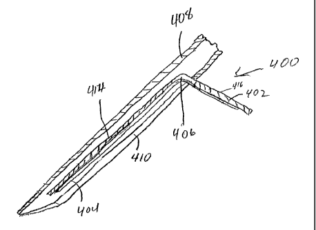
FIGS. 26-29 illustrate a sensor 400 formed in accordance with another
einbodiment of the present invention. The sensor 400 includes a substrate 402
and at least one sensor electrode 404 formed from one or more conductive
layers.
In particular embodiments, the layers are formed from metal. However,
alternative embodiments may utilize semiconductors, conductive polymers, DNA,
RNA, molecular wires, or the like. The substrate 402 and the sensor 404 are
formed and process by methods similar to those described above in tl-ie other
embodiments. However, in this embodiment, the substrate 402 is formed from a
thiclcer film (from a reel or as a sheet) so that no bead is required. The
thickness
of the substrate ranges from approximately 25 to 350 . In further
embodiments,
thicker films may be used up to 750 or thinner films down to 5 may be used,
with the thickness being determined by the strength of the substrate 402
material,
- 23 -
CA 02395868 2002-06-21
WO 01/58348 PCT/US01/04270
the substrate material's resistance to tearing, the flexibility of the
substrate
material, or the like. For instance, if the substrate is contained within a
slotted
needle (or supporting structure) during insertion, a comparable normal or
thinner
thickness to the other embodiments described above may be used.
The sensor 400 is formed to obviate the need for a sensor set housing that
remains attached to the body or the use of an additional bead, as described
above
in FIGS. 5-25b. To achieve this capability, the substrate 402 is formed (or
cut) to
include one or more notches 406. The notches 406 create a necked down region
in the sensor 400 that allows the sensor 400 to slide into a slotted needle
408 that
has a slot 410 that is narrow enough to permit passage of the necked down
region
412 of the sensor 400, but prevent the non-necked down region 414 of the
sensor
400 from pulling out of the slotted needle 408 through the slot 410. The slot
410
does permit the necked down region 412 of the sensor 400 to slide down the
slot
410.
To insert the sensor, a sensor 400 is placed inside a slotted needle 408 by
sliding the necked down region 412 into the slot 410 of the slotted needle 408
so
that the non-necked down region 414 is slid up and into the interior of the
slotted
needle 408, while a connection region 416 remains outside of the slotted
needle.
The slotted needle 408, including the sensor 400, is inserted into a body (not
shown). The sensor 400 is held against the body by the connection region 416
and the slotted needle 408 is then pulled out of the body (alternatively, the
sensor
may be included in a sensor set that holds the needle and the sensor). As the
slotted needle 408 is pulled from the body, the necked down region 412 slides
down the slot 410 of the slotted needle 410 and remains implanted in the body.
Thus, in this embodiment, a sensor set and bead are not required, and the
substrate 402 is of sufficient strength to remain in the body without any
other
support structures. In particular embodiments, the sensor may fit within a 21
gauge to a 27 gauge slotted needle for easy insertion into the skin.
In an alteniative of these embodiments, to provide for the manufacture of
a narrower sensor in width, with the aim to further minimize the size of the
needle used to surround the sensor during insertion, several different
approaches
to sensor electrode layouts may be used. In one embodiment, two electrodes 502
-24-
CA 02395868 2002-06-21
WO 01/58348 PCT/US01/04270
and 504 are formed on one side 506 of the sensor 500 and a single electrode
508
is formed on the other side 510 (see Figs. 30(a) and 30(b)). This allows the
size
of the electrodes to be maintained with a consuinmate reduction in width. In
further alternative embodiments, one electrode 552 is formed on one side 554
of
the sensor 550 and another single electrode 556 is formed on the back 558 of
the
sensor 550 (see Figs. 31(a) and 31(b)). A third electrode 560, if needed, such
as a
ground (or reference) electrode is formed before the necked down region of the
sensor to form an electrode that rests on (or is in contact with) the top of
the skin
(see Fig. 31(a). This substantially reduces the width of the sensor permitting
small gauge needles to be used. For instance slotted needles of 22 gauge to 28
gauge may be used.
While the description above refers to particular embodiments of the
present invention, it will be understood that many modifications may be made
without departing from the spirit thereof. In particular, it is to be
understood that
the exemplary embodiments set forth herein, whether refelTed to as preferred
embodiments or otherwise, are in no way to be taken as limiting the scope of
the
present invention. The accompanying claims are intended to cover such
modifications as would fall within the true scope and spirit of the present
invention.
The presently disclosed embodiments are therefore to be considered in all
respects as illustrative and not restrictive, the scope of the invention being
indicated solely and exclusively by the appended claims, rather than the
foregoing description, and all changes which come within the meaning and range
of equivalency of the claims are therefore intended to be embraced therein.
-25-