Note: Descriptions are shown in the official language in which they were submitted.
CA 02396082 2009-07-15
67789-473
ARC-LESS ELECTRICAL CONNECTOR
BACKGROUND OF THE INVENTION
Field of the Invention
This invention relates to an electrical connector including means for
preventing or suppressing an arc when power contacts are disconnected or
separated
while they carry substantial power or electrical current. This invention also
relates to
an electrical connector that preferentially uses a positive temperature
coefficient
resistor shunted between contacts that are disconnected sequentially so that
voltage
and current will be below a threshold at which arcing might occur, when each
contact
is separated from a mating contact.
Description of the Prior Art
Contacts carrying significant amounts of power will arc when disconnected.
The amount of arc damage experienced by the contacts depends on their physical
structure, the load current, the supply voltage, the speed of separation, the
characteristics of the load (resistive, capacitive, inductive) as well as
other factors.
Future automotive systems are expected to utilize 42 volts in order to reduce
the load currents and the associated wiring losses. This increased voltage
could cause
significant arc damage to occur to the present connectors designed for 12-volt
operation. To avoid the possible liabilities associated with catastrophic
connector
failure, automotive manufacturers are requesting a new connector design that
can be
hot-swapped some significant number of times. Ten cycles is considered to be a
minimum requirement.
To disconnect 42-volt power without significant damage requires interrupting.
about 1500-watts for many loads and as much as 15 KW for the main battery
circuit.
Present day modules used in automotive applications can consume more than 500
1
CA 02396082 2009-07-15
67789-473
watts. Power supplies must deliver one or more kilowatts of energy.
Conventional
solutions require either that the current be shut off before the contacts are
separated or
unmated or employ a sacrificial contact portion. The cost, space, reliability,
safety,
performance and complexity of these conventional solutions make them
unsuitable
for many applications, including automotive electrical systems.
There are many things known in the power utility profession that will quickly
extinguish an arc and there are many things known in the relay industry that
will
minimize arc damage to connectors and contacts. These can be found. in
literature,
such as Gaseous Conductors by James D. Cobine (McGraw-Hill, 1941) and the
Ney_Contact
Manual by Kenneth E. Pitney (J.M. Ney Co., 1973). Most of these methods are
not practical in
smaller and separable electrical connectors such as those used in automobiles,
computers and
appliances. None of the methods provided in the literature will eliminate
arcing. Conventional
contacts will be destroyed when rated currents are interrupted often enough
and
slowly enough, even though these conventional contacts may rated for current
interruption. There is a finite life for existing connectors since arcing will
occur and
cause damage each time the connector is disconnected under load.
Positive Temperature Coefficient Resistance (PTC) Devices, resistorsor
switches have been used, or suggested for use, in circuit breakers that are
used to
break fault currents, specifically defined and excessive overcurrents, for
which these
circuit breakers are rated. On the other hand, electrical connectors are
expected to
carry a wide range of currents during actual use. Even though an electrical
connector
may be rated to carry a specific current, in actual practice, an electrical
connector will
carry currents over a large range due to variations in the load. The cost,
size and
weight of an electrical connector will generally increase with increasing
current
rating, so the lowest rated connector suitable for use in a specific
application will
normally be used. Because multiple loads with different current needs pass
through a
single connector, as well as for economic, inventory and.connector product
line
consistency, it is not uncommon to minimize the number of different connectors
utilized in a specific product. The net result, is that a specific connector
will carry
anywhere from its rated current, or even an overcurrent for safety and life
testing, to
some significantly lower current. If that connector is to be disconnected
while
carrying a current, or hot swapped, without arcing, arc prevention must be
effective
for a large range of currents, starting from the arc threshold current to the
rated
current for that connector. In other words, unlike circuit breakers, hot
swapped
2
CA 02396082 2009-07-15
67789-473
connectors must be protected from arcing over a wide range of currents.
Therefore
use of a PTC resistor in the same manner as it is used in a circuit breaker
will not be
suitable for use in an electrical connector. The trip time varies for a PTC
device in
which resistance is dependent upon the temperature of the device, and the
temperature
is dependant upon current because of IZR heating. Thus the trip time for a PTC
device
used in an electrical connector will vary because of the wide range of
currents that
will be carried by a particular electrical connector.
When PTC resistance devices are used in switches, relays, fuses and circuit
breakers, both halves of electrical contacts remain within the same physical
device.
The contacts separate from each other, but only by a well defined and fixed
distance,
and the separated contacts are still part of the device package. The essential
function
of electrical connectors is to totally separate the two contact halves. No
physical
connection remains between the two halves, and all physical ties are broken
between
two mating connector contacts. In order to protect separating electrical
contacts that
are carrying arc-producing power, the PTC device must be connected across the
contact pair until the current is sufficiently reduced to prevent arcing.
Thus, the
problem is that a physical electrical connection to both halves of the
separating
electrical contact must be maintained in a conventional use of a PTC device
yet, in a
connector, all physical connections must be broken.
In switches, relays, fuses and circuit breakers, where prior art PTC devices
are
used; the distance of contact separation and the rate of separation are
controlled. In
these prior art devices, the contact separation needs to only be enough to
hold off the
rated voltage. The rate of separation can be made as fast as possible to
shorten the
time in which arcing could occur, therefore minimizing any associated damage.
Electrical connectors must be completely separated. Electrical connectors are
also
manually separated, and the rate of separation varies widely for existing
electrical
connectors. Even for a specific manually separated electrical connector
design, the
rate of separation will vary significantly each time two electrical connectors
are
manually unmated.
SUMMARY OF THE INVENTION
To overcome these problems, some embodiments of the instant invention employ a
positive temperature coefficient (PTC) resistor in an electrical connector in
series with
3
17722 CA 02396082 2002-07-31
an auxiliary electrical contact portion or contact terminal, the combination
of which is
in parallel with a main electrical contact portion or contact terminal, which
disconnects first. This arrangement of components parts will prevent arcing
when
two electrical connectors are unmated while carrying current. Both the main
and the
auxiliary contacts are matable with a terminal or terminals in a mating
electrical
connector. In the preferred embodiments, the main and auxiliary contacts are
male
terminals or blades that mate with a female or receptacle terminal in the
mating
electrical connector. However, the PTC resistive member could also be employed
with the female terminals. The PTC resistive member should, however, only be
employed with the terminals in one half of a mating pair of electrical
connectors. The
main or auxiliary contact portions or terminals in one of the two connectors
must
incorporate the PTC member. When a conventional discrete PTC member, such as a
commercially available POLYSWITCH device, is used, the main and auxiliary
contact portions or terminals in the other of the two mating connectors must
be
connected together directly, with no discrete PTC device between them.
However, in
other applications the PTC means may be located in both connectors.
A discrete PTC resistive member can be employed into the main and auxiliary
contact terminals so that the PTC device can form an integrated unit.. One
means for
forming such an integrated unit would be to mold a PTC conductive polymer
between
2o the main and auxiliary contact terminals. The PTC conductive polymer could
also be
overmolded around portions of the main and auxiliary contact terminals, with
the PTC
conductive polymer being molded between the main and auxiliary contact
terminals.
Insert molding techniques could be used to position the PTC conductive polymer
between, the main and auxiliary contact terminals. The PTC conductive polymer
could also be a discrete component that is molded as a shape that would
conform to
parts of the main and auxiliary contact terminals and this discrete component
could be
bonded between the main and auxiliary contact terminals using solder, a
conductive
adhesive or some other conductive bonding agent.
The main contact should unmate before the auxiliary contact, and in the
_;o representative embodiments depicted herein, the auxiliary contact is
longer than the
main contact. In the preferred embodiment, the PTC member comprises a
conductive
polymer member in which conductive particles are contained within a polymer
matrix. Normally the conductive particles form a conductive path that have a
resistance that is larger than the resistance of the main terminal so that
under normal
4
_ . .~ ....a.... ~:... .. _.. ....
CA 02396082 2009-07-15
67789-473
mated operation, the main contact would carry substantially all of the
current.
However, as current increases in the PTC member, the polymer expands and the
resistance increases. When current through the PTC member increases rapidly
due to
disconnection of the main contact terminal, the resistance will increase
rapidly due to
12R heating of the polymer. To prevent arcing when the main contact is
unrnated, the
disconnect time for the main contact must be less than the time for the
resistance of
the PTC member to increase too greatly. Most of the current through the main
contact
must be carried by the PTC member and the auxiliary contact until the main
contact
has moved to a position in which arcing is no longer possible. Before the
auxiliary
1o contact is disconnected from the mating terminal, the resistance in the PTC
member
must increase so that the current flow through the auxiliary contact will drop
below
the arcing threshold before the auxiliary contact is unmated. This time is
called the
trip time of this PTC resitive member. Since the trip time of the PTC member
will
depend on the initial current through the main contact, which can vary over a
wide
range, the trip time for a given electrical connector will therefore not be
constant. To
insure that the PTC member will trip, the electrical connector of this
invention
employs latches that cannot be activated, after the disconnection of the main
contact,
for a time interval that will be greater than the maximum trip time for the
PTC
member. However, these latches must also permit rapid movement between the two
2o electrical connectors as the main contact moves through a portion of its
path in which
it is susceptible to arcing. Similarly, the auxiliary contact must move
rapidly through
an arc susceptible region as it is disconnected. The preferred embodiments of
this
invention therefore use multiple sets of latches that must be sequentially
disengaged,
and which provide a time delay between disconnection of a first set of latches
and the
disconnection of a second set of latches. This time delay should be longer
than the
maximum PTC trip time. This multiple latch configuration provides a versatile
implementation of the invention. If, however, a specific electrical connector
serves
loads with a small difference between maximum and minimum current loads, a
simpler latch mechanism can be utilized. The maximum achievable parting
velocity
and the added length of the auxiliary contact could in some cases provide
adequate
time for the PTC device to trip.
5
CA 02396082 2009-07-15
67789-473
According to one aspect of the present invention, there is provided
an electrical connector matable to and separable from a separate mating
electrical
connector, the electrical connector including first and second contacts and a
variable resistance member connecting the first and second contacts, the
variable
resistance member providing a shunt so that arcing does not occur when the
first
contact is disconnected from a mating terminal in the separate mating
electrical
connector, wherein the variable resistance member comprises a positive
temperature coefficient resistance member.
According to another aspect of the present invention, there is
provided an electrical connector matable to and separable from a separate
mating
electrical connector, the electrical connector comprising; a main contact
member;
an auxiliary contact member; a variable resistive member connected between the
main contact member and the auxiliary contact member, and disconnect means
for discontinuously disconnecting first the main contact member and then the
auxiliary contact member from terminal means in the mating electrical
connector
to reduce arcing when separation of the electrical connector from the mating
electrical connector disconnects current through the electrical connector.
According to still another aspect of the present invention, there is
provided an electrical connector matable to and separable from a separate
mating
electrical connector, the electrical connector comprising: a main contact
terminal
including means for connecting the main contact terminal to an electrical
conductor; an auxiliary contact terminal; and a resistive member connecting
the
auxiliary contact terminal to the main contact terminal, such that current
passing
through the auxiliary contact terminal also passes through the main contact
terminal and the resistive member, the resistive member being characterized in
that an increase in electrical resistance of the resistive member lags an
inrush
current through the resistive member, so that the resistive member carries a
current approximately equal to the inrush current for a period of time
referred to as
a trip time, wherein the resistive member comprises a positive temperature
coefficient resistive member; the electrical connector being configured to
disconnect the main contact terminal from a mating electrical terminal in the
separate mating electrical connector prior to disconnection of the auxiliary
contact
5a
_ : . ,. . , . . .,~., _ _ ,.w... . . , . .
CA 02396082 2009-07-15
67789-473
terminal from a mating electrical terminal in the mating electrical connector,
the
time to disconnect the main contact terminal by a distance sufficient such
that an
electrical arc cannot be sustained comprising a disconnect time, the
disconnect
time being less than the trip time so that arcing is prevented upon
disconnection of
the main contact terminal.
According to yet another aspect of the present invention, there is
provided an electrical connector matable to and separable from a separate
mating
electrical connector, the electrical connector comprising: a main contact
terminal;
an auxiliary contact terminal; a switch comprising a positive temperature
coefficient resistance member connected between the main contact terminal and
the auxiliary contact terminal, the switch being characterized by a finite
trip time to
switch from a first relatively low resistance state to a second relatively
higher
resistance state; the electrical connector being configured so that the main
contact
terminal is separable from a mating terminal in the separate mating electrical
connector in a disconnect time that is less than the trip time to reduce
arcing when
the main contact terminal is disconnected when current flows through the
electrical connector and the separate mating electrical connector,
disconnection of
the auxiliary contact being delayed relative to disconnection of the main
contact by
a sufficient time so that both the main contact and the auxiliary contact can
be
disconnected without arcing.
According to a further aspect of the present invention, there is
provided an electrical connector that can be disconnected, without damage due
to
arcing, from a separable mating electrical connector while carrying electrical
energy above an arcing threshold, the electrical connector comprising: a main
contact matable with and unmatable from a mating contact in the mating
electrical
connector; at least one auxiliary contact; a positive temperature coefficient
resistor
between the main contact and the auxiliary contact; the main contact being
separable from the mating contact before the auxiliary contact is disconnected
from a circuit including the mating contact in the mating connector so that
the
resistance in the positive temperature coefficient resistor increases after
disconnection of the main contact from the mating contact and prior to
5b
..... . ... .. . . .:. , . ,,. ,. . .... . . , :.:.,,_. ... .:.w.~,
,.....:...,....cw.w...,....,..,,,.,m-,. , :........ ., ...... ..._ _. . ..
CA 02396082 2009-07-15
67789-473
disconnection of the auxiliary contact from the circuit so that both the main
contact
and the auxiliary contact can be disconnected without arcing.
According to yet a further aspect of the present invention, there is
provided an electrical connector matable to and unmatable from a separate
mating connector, the electrical connector comprising: a main contact; an
auxiliary
contact; a variable resistance positive temperature coefficient member between
the main contact and the auxiliary contact; a first latch disengagable from
the
mating connector, to disconnect the main contact from mating terminal means in
the mating connector; a second latch disengagable from the mating connector
after the main contact has been disconnected from the mating terminal means,
the
auxiliary contact being disconnectable from a mating terminal means in the
mating
electrical connector upon disengagement of the second latch.
According to still a further aspect of the present invention, there is
provided an electrical connector disconnectable from a separate mating
electrical
connector without arcing, the electrical connector comprising: main contact
means
and auxiliary contact means, each matable with and unmatable from mating
terminal means in the mating electrical connector as the electrical connector
is
separated from the mating electrical connector; resistive means comprising
positive temperature coefficient resistive means between the main contact
means
and the auxiliary contact means, the main contact means comprising a lower
resistance path than a path through the resistive means and the auxiliary
contact
means; the electrical connector being configured so that, when the electrical
connector is unmated and separated from the mating electrical connector, the
main contact means is disconnected from the mating terminai means in the
mating
electrical connector before disconnection of the auxiliary contact means and
the
mating terminal means so that a current path through the auxiliary contact
means
and the resistive means to the mating terminal means remains intact after
disconnection of the main contact means from the mating terminal means; the
resistance through the resistive means and the auxiliary contact means being
greater when the auxiliary contact means is disconnected from the mating
terminal
means than when the main contact means is disconnected from the mating
terminal means so that arcing does not occur when the main contact means and
5c
... w__,
CA 02396082 2009-07-15
67789-473
the auxiliary contact means are sequentially disconnected from the mating
terminal means.
According to another aspect of the present invention, there is
provided an arc avoidance electrical connector disconnectable and separable
from
a mating electrical connector under load, the electrical connector including:
a main
contact disconnectable from a mating terminal in the mating electrical
connector
as the mating electrical connector is unmated and separated from the
electrical
connector; shunting means for shunting sufficient current through an alternate
path to the mating electrical connector as the main contact is disconnected
from
the mating terminal so that arcing does not occur as the main contact is
disconnected from the mating terminal, wherein the shunting means includes a
positive temperature coefficient resistive member.
According to yet another aspect of the present invention, there is
provided an electrical connector matable to and separable from a separate
mating
electrical connector, the electrical connector comprising; a main contact
member;
an auxiliary contact member; a variable resistive member connected between the
main contact member and the auxiliary contact member, wherein the variable
resistive member comprises a positive temperature coefficient resistive member
and disconnect means for disconnecting first the main contact member and then
the auxiliary contact member in two stages to reduce arcing when disconnection
of the electrical connector disconnects current through the electrical
connector.
BRIEF DESCRIPTION OF THE DRAWINGS
5d
17722 CA 02396082 2002-07-31
Figure 1 is a view of the stages that a representative electrical connector
terminal, according to this invention, will pass while being unmated.
Figure 2 is a view of mating contact terminals, according to a configuration
used to demonstrate the characteristics of an electrical connector employing
this
invention.
Figures 3A-3C are representative plots showing the trip times for various
currents of electrical connector terminals according to this invention.
Figure 4 is a plot showing the variation of trip time to current.
Figure 5 is a view of mated plug and header electrical connectors, according
to
the first embodiment of this invention, showing the position of a PTC device
connected between two contact terminals.
Figure 6 is a view of two unmated electrical connectors incorporating the
first
embodiment of this invention, and the terminals shown in Figure 5.
Figure 7 is a view of the mated configuration of the two electrical connectors
shown in Figure 6.
Figure 8 is a view of the mating face of a plug connector incorporating
receptacle contact terminals according to this invention.
Figure 9 is a three dimensional view of the plug connector shown in Figure 8
showing the sequential latches employed in the first embodiment of this
invention.
1.o Figure 10 is a view of a header connector housing, matable with the plug
connector shown in Figures 8 and 9.
Figure 11 is a three dimensional view of the header shown in Figure 10,
showing two latching detents that are located at different positions along the
mating
axis of the electrical connector.
Figure 12 is a three dimensional view of a receptacle contact terminal
comprising a second embodiment of this invention.
Figure 13 is a three dimensional view of a blade contact terminal comprising a
second embodiment of this invention.
Figure 14 is a view in which the mating terminals of Figures 12 and 13 are
3o aligned prior to mating.
Figure 15 is a side view of the mating terminals shown in Figure 14.
Figure 16 is a top view of the mating terminals shown in Figures 14 and 15.
Figure 17 is a view of the auxiliary contact terminal of the second embodiment
of this invention.
6
17722 CA 02396082 2002-07-31
Figure 18 is a view of the main contact terminal of the second embodiment of
this invention.
Figure 19 is a view showing the manner in which the main and auxiliary
contact terminals are position so that a PTC material can be overmolded.
Figure 20 is a view of the matable plug and header connectors according to the
second embodiment of this invention.
Figure 21 is another view of the mating plug and header connectors of Figure
20.
Figure 22 is a view showing the plug and header connectors of Figures 20 and
21 in a fully mated configuration.
Figure 23 is a view of the mating face of the plug connector housing of the
embodiment also shown in Figures 20-22.
Figure 24 is a view of a lever that is used with the plug connector housing of
Figure 23.
Figure 25 is a view of the mating face of the header housing of the
embodiment of Figures 20-23.
Figures 26-32 show the mating sequence of the two connectors of the second
embodiment of this invention.
Figure 26 is a side view of the two mating connectors of the second
1.o embodiment in a first mating position, showing the application of a force
for initially
mating the two electrical connectors.
Figure 27 is a three dimensional view of the two mating connectors in the
position also shown in Figure 26.
Figure 28 is a detail view showing the position of the mating assist lever
when
the two connectors are in the position shown in Figures 26 and 27.
Figure 29 is a side view of the two connectors of the second embodiment in a
second position, showing application of a force to the mating assist lever.
Figure 30 is a three dimensional view of the two connectors in the position of
Figure 29.
:so Figure 31 is a view of the two connectors of the second embodiment,
showing
the two connectors in a fully mated configuration and also showing the manner
in
which the lever can be unlocked.
Figure 32 is a three dimensional view of the two connectors in the position
also shown in Figure 31.
7
17722 CA 02396082 2002-07-31
Figures 33-37 show the unmating sequence for the two connectors of the
second embodiment.
Figure 33 is a side view of the two connectors in an intermediate position in
which the lever has been unlatched. This figure illustrates the position in
which the
lever can be used to disconnect the main contact. Figure 34 is a three
dimensional
view of the two connectors in the position also shown in Figure 33.
Figure 35 shows the way in which latches are disengaged, after the lever has
been rotated to its final position, so that the auxiliary contact terminal can
be
disengaged. The main contact is fully disengaged in this stage of the unmating
cycle.
Figure 36 is a three dimensional view of the two connector in the position
also
shown in Figure 35.
Figure 37 shows the two connectors in a fully unmated position.
Figure 38 is a photograph showing the damage that would occur when one
prior art connector configuration is disconnected one time at 59V, while
carrying a
current of 60 Amps.
Figure 39 is a photograph showing a contact terminal configuration similar to
that shown in Figure 38 in which the instant invention has been employed to
protect
the mating sections of the terminals after they have been disconnected fifty
times at
59 Volts, while carrying a current of 60 Amps.
Figure 40 is a schematic representation of a means to protect an electrical
system from the over-voltage effects of an inductive load.
Figure 41 is a schematic representation of a second means to protect an
electrical system from the over voltage effects of an inductive load.
Figures 42A-42D show and alternate embodiment in which a connector
assembly employs a lever that provides rapid unidirectional movement through
the
contact disconnect zones and the time delay between them with a single lever.
DETAILED DESCRIPTION OF THE PREFERRED EMBODIlViENTS
A series of complex events lead to damaging arcs as contacts are separated
while carrying substantial power. A simple description of the major events
that occur
in typical power contacts helps understand this phenomenon. First, as the
contacts
begin to separate, a point is reached where there is no longer enough metallic
area to
support the current flow. A very small molten bridge forms and breaks as the
8
. .. _ .. i ... ..... . . . .. .. . _ ... .. . . .__.. . , , .wõ _~ ._..._ .~-
t....._. ._ ... . . . -. _ . . .~ . . _. ~_ . ..._ ._. . . . . .._. . . . _ .
,._ _.
CA 02396082 2009-07-15
67789-473
temperature and separation distance increase. Generally, this can occur at
currents
above 0.1 ampere and voltages greater than 9 volts. Enough current is needed
to
cause the melting and enough voltage is needed to sustain it and move to the
next
phase. As the molten micro-bridge boils and breaks, electrons are freed and
current
continues to flow by ionizing the intervening atmosphere. A true arc is the
next
result. This true arc consists of several sub-parts including the cathode
spot, the
cathode drop region, an extremely hot plasma channel, the anode drop region
and the
anode spot. The plasma channel is about 5000 C and the anode and cathode
spots
reach about 2000 C at 10-20 ampere currents.
If arcing is permitted to occur, mating contacts will be damaged. The degree
of damage is controlled by many factors that determine the total arc energy.
Priinary
ways to limit the arc energy are to minimize the current and voltage and by
maximizing the separation velocity. There may be other means, but they do not
lend
themselves well to applications in which typical connector designs are
utilized. For
ordinary connectors, the only factor that can be controlled to a significant
extent is the
separation velocity.
By integrating a Positive Temperature Coefficient (PTC) resistance member
into a two-piece contact, the voltage and current can be kept below the arcing
threshold voltage and current when two connectors are unmated. This produces a
contact that will not arc while interrupting significant energy as the
connectors are
disconnected. A PTC device, such as a discrete PTC resistor exemplified by a
RHE
110 POLYSWITCH device manufactured and sold by the Raychem division of
Tyco Electronics Inc. may be employed. POLYSWITCH is a registered trademark
of Tyco Electronics Inc. The leads of the discrete device can be soldered to
the
respective main and auxiliary contacts. The leads on a discrete device could
also be
attached by contact springs or by crimps or by latching detents on the
contacts. A
conductive polymer, of the type exemplified by this discrete device can also
be
overmolded onto contact terminals to form a new component, or a PTC device can
be
integrated with the contact terminals to form an integrated component or unit.
This
approach may not eliminate the relatively benign spark that may occur when a
high-
energy circuit is connected. In the energy range of interest, this benign
spark tends to
do little damage to the contact base metal and to the shape of the contact.
The general
characteristics of POLYSWITCH devices are discussed in US Patent 5,737,160,
US Patent 5,737,160 and the other
9
CA 02396082 2009-07-15
67789-473
patent incorporated therein are in turn incorporated herein by reference for
all
purposes. The formulation of a conductive PTC device of the type used in a
discrete
POLYSWITCH device is discussed in US Patent 6,104,587.
This same formulation can also be used to form the conductive
PTC polymer that can be molded into a shape compatible with the main and
auxiliary
contacts, or the PTC polymer can be overmolded or insert molded with the
contact
terminals as subsequently discussed with respect to the representative
embodiments
depicted herein.
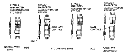
Figure 1 shows the concept for an arc-less power contact in accordance with
the instant invention. Representative male and female, or blade and receptacle
terminals, according to this invention, are shown in various stages of
disconnection or
unmating. There are three important components of the power contact
illustrated in
Figure 1. The main contact, or the main portion of the contact, carries the
load
current during normal operation. The main contact is shunted by a series
connected,
longer auxiliary contact or contact portion and by a positive temperature
coefficient
resistance or resistor, located between the main contact and the auxiliary
contact.
Figure 1 illustrates the four stages that occur during separation of the plug
connector from the mating receptacle connector. In stage 0, the contact is
carrying a
high current. The current is primarily flowing through the main contact or the
main
portion of the contact. Only a relatively small shunt current flows through
the series
connected positive temperature coefficient resistance or resistor (PTC) and
the
auxiliary portion of the contact. Stage 0 represents the normal operating
configuration of a connector assembly. Relative movement of the two contacts
in this
position would result in the normal wiping action between two contact
surfaces.
Stage 1 shows the configuration in which the main contact or main contact
portion has been separated or disconnected from the mating contact in the
other
connector. The main blade is separated from the main receptacle through the
main
contact disconnect zone (MDZ), which occurs between Stage 0 and Stage 1, in
which
the main blade contact is in the process of unmating from the corresponding
female or
receptacle contact. While the two contacts are in this main disconnect zone,
the two
contacts are not completely separated. Contact bounce may occur as the spring
members flex and as irregular surfaces on the contact result in momentary
separation
and engagement. It is while the main contact and the receptacle contact are in
this
contact disconnect zone (MDZ) that arcing between the two connectors is most
likely,
17722 CA 02396082 2002-07-31
since a relatively large existing current is being disconnected. For a
conventional
prior art connector, arcing could occur across a small gap in the MDZ, if the
voltage
and current are above an arcing threshold for the particular connector
configuration.
However, in the instant invention, the voltage and current across the opening
gap are
limited by the positive temperature coefficient (PTC) resistor or resistance
and the
auxiliary contact or contact portion. Duration of the MDZ should be less than
the trip
time for the PTC device so that the PTC device does not switch to an OFF or
open
condition before completion of the separation between the contacts.
When the mating contacts have moved to the position identified as Stage 1, the
to main contact is physically separated from its mating contact so that arcing
can no
longer be initiated. Since there was only a small amount of current flowing
through
the PTC resistor during Stage 0, the IZ R heating remained low causing the
resistance
of the PTC resistor to be in a low state when the contacts reached the
position
identified as Stage 1. Since the resistance is relatively low, current flows
through the
PTC resistor to the auxiliary contact and the PTC, which acts like a switch,
can be
said to be ON. While the auxiliary contact or auxiliary contact portion
remains
connected to the mating contact in the mating connector or to the same circuit
in the
mating connector, the current through the PTC resistor and the auxiliary
contact will
be greater than in Stage 1 and therefore IZ R heating will increase. The
resistance of
zo the PTC resistor increases with increasing temperature. Stage 2 illustrates
this
configuration in which the longer auxiliary contact remains connected to the
mating
contact as physical unmating or relative movement between the connectors and
contact terminals continues. Stage 2 illustrates a snapshot of one position of
the
contacts during the time after the main contact is separated and before
disconnection
of the auxiliary contact. It is during Stage 2 that the PTC resistor will open
or, in
other words, its resistance will significantly increase. Therefore, the PTC
switch is
now in the OFF position.
Prior to the time that the auxiliary contact separates from the mating
contact,
or from the circuit including the mating contact, the current flowing through
the
:30 auxiliary contact will be below the arcing threshold. This is due to the
increased
resistance of the PTC during the time when relative movement of the two
terminals or
connectors occurs. This range of movement within the disconnect travel is
called the
PTC Opening Zone. When the auxiliary contact finally separates at Stage 3,
there is
only a small amount of leakage current flowing through the connectors. At this
point
I1
17722 CA 02396082 2002-07-31
there will be insufficient electrical energy to support an arc between the
auxiliary
contact portions.. Enough time should elapse while the terminals or connectors
are in
the PTC opening zone, so that the current is below the arcing threshold before
the
auxiliary contact is physically disconnected from the receptacle contact in
the
Auxiliary Disconnect Zone (ADZ). Stage 3 shows the mating contacts completely
separated and disconnected with both the main contact and the auxiliary
contact
open. Since current is no longer flowing through the connectors, the PTC
resistor will
return to the RESET state of lower temperature and resistance. The contact
assembly
will then be in a state so that they will again function so that arcing will
not occur
when the connectors are unmated under load.
Preferably, this contact configuration is employed in a connector housing that
provides velocity control to assure that the timing of the stages illustrated
in Figure 1
will be appropriate. The housing should also assure that unmating velocity is
unidirectional. That is to say there should be no macro break-make-break
action of
the main contact as the connector separates. Nanosecond or micro
discontinuities will
occur, but these micro break-make-break actions will not interfere with the
arc
protection because the PTC resistor will be chosen to react much slower than
these
relatively high speed events. All four stages should be passed in a
unidirectional and
sequential manner.
The blade contact of Figure 1 mates with the receptacle contact, which has
flexible spring beams mating with the plug or blade contact. The plug or blade
contact includes a main contact or main contact portion and an auxiliary
contact or
auxiliary contact portion. In this embodiment, the main contact and the
auxiliary
contact are two separate metal blades that each engage separate spring beams
on the
receptacle contact. In this representative configuration, the receptacle
contact
comprises a single piece metal member with separate spring beams engaging the
main
contact and the auxiliary contact respectively. The main contact and the
mating
receptacle contact are each printed circuit board style contacts with multiple
leads
extending from rear ends of each contact. The auxiliary contact or blade does
not
_SO include means, such as the PCB leads, for connection to the external
circuit
independently of the main contact. The PTC resistor employed in this invention
can
comprise a molded member that can be bonded along at least one side to the
central
section of the main contact. A suitable conductive adhesive can be employed if
necessary. The auxiliary contact is bonded to the PTC resistor along another
side so
12
17722 CA 02396082 2002-07-31
that the PTC member is located physically and electrically between the main
contact
and the auxiliary contact. Stages 0-3 show the relative positions of the
contacts as a
connector in which these contacts are included are unmated. The PTC member
employed herein preferably comprises a conductive polymer that can be molded
to the
desired shape. Conductive particulate fillers, such as carbon black, are
dispersed in a
nonconductive polymer to form a conductive path having a resistance that is
dependent upon the temperature and state of the polymer. Devices employing a
conductive polymer are well known and are available from Tyco Electronics.
These
POLYSWITCHO devices are employed in other applications. Barium-Titanate or
semiconductor material exhibiting PTC behavior might also be employed, but
these
alternative PTC materials may prove too expensive for practical use in
electrical
connectors.
Figure 2 is a view of a sample contact terminal configuration 2 that is used
to
demonstrate the performance of this invention when terminals are cycled in the
manner shown in Figure 1. The sample configuration shown in Figure 2 includes
two
male terminal blades 12, 16. A main terminal blade 12 is connected in series
to a
longer auxiliary terminal blade 16 by a discrete PTC device 6. In this
configuration a
PTC device having characteristics generally equivalent to a Tyco Electronics
RHE
110 is employed. Leads 8 are soldered to the main and auxiliary terminal
blades 12,
10 16. These terminal blades 12, 16, connected in series by the PTC device,
can be
mated with and unmated from two receptacle terminals 32, 36, which will be
connected in parallel to a common external conductor. Each of the main
terminals
12 and 32, shown in Figure 2 can continuously carry all of the current
employed
herein. The auxiliary terminals 16, 36 carry the full current only for as long
as it takes
for the POLYSWITCHO device to trip or open. The two receptacle terminals 32,
36
can be considered to represent one terminal having multiple spring members 34
A, B
and 38A for contacting two separate blades 12, 16. The auxiliary blade 16 is
longer
than the main blade, so it will connect first and disconnect last from the
receptacle
terminal assembly 30.
Figures 3A to 3C and Figure 4 show the relationship between current and trip
time for a connector and contact terminal using a PTC resistance device in the
manner
described herein. Figures 3A through 3C are plots showing waveforms of the
voltage
as mating contacts were disconnected under power. Figure 3A shows the results
of
the second and tenth cycling for contacts that were cycled with two amps being
13
17722 CA 02396082 2002-07-31
carried by the mating contacts. Figure 3B shows the results of the second and
tenth
cycle for the same contact configuration in which five amps were carried by
the
mating contacts. Figure 3C shows waveforms for a ten amp test in which the
first,
tenth, thirty-third, thirty-sixth and fiftieth cycles are recorded. Figure 3C
also shows
the difference between waveforms in which no arcing occurred and in which
arcing
occurred when the PTC material was not permitted to return to its ON condition
before the contacts were again disconnected.. Comparison between these
waveforms
in Figure 3C, shows the effectiveness of the the PTC material. Comparison of
Figures
3A - 3C shows that the time to disconnect the two mating contact terminals
differed
for different currents. In other words, the unmating velocity was not the same
for
each waveform. Trip-time for the PTC resistance device, used herein, as a
function of
current is shown in Figure 4.
Figures 5-11 show an electrical connector assembly 4 that can be employed
with the contact configuration 2 of Figure 2 and with a discrete conductive
polymer
PTC device or switch 6, such as the Tyco Electronics RHE110.. Figure 5 shows a
portion of a mated header and plug connector configuration 4 in which a
discrete
conductive polymer PTC device 6 is employed. The discrete PTC device 6 is
inserted
into a pocket 48 formed on the rear or printed circuit board side of a molded
receptacle header housing 42. This pocket 48 retains the conductive polymer
PTC
device 6, but it provides sufficient space to permit the PTC device 6 to
expand. The
leads 8 on the discrete PTC device 6 are soldered directly to a rear portion
14 of the
main contact member 12 and to a rear portion 18 of the auxiliary contact
member 16
In this configuration only the main contact member 12 in the header 40 would
be
attached directly to an external conductor on a printed circuit board. The
auxiliary
contact member 16 would not be connected to an external conductor through the
printed circuit board. Its only contact with an external conductor would be
either
through the discrete PTC member 6, or in the mated configuration, through the
auxiliary receptacle terminal 36 to which it is mated.
Figures 6 and 7 show the manner in which this embodiment insures that the
:3o PTC resistive device 6 is in the proper state during disconnection of the
main contact
12 and disconnection of the auxiliary contact 16. The plug connector housing
52 and
the header housing 42 of Figures 6 and 7 have two separate latching mechanisms
that
must be independently actuated in order to unmate the plug connector 50 from
the
header 40. As seen in Figures 6-9, the plug connector housing 52 has two
separate
14
17722 CA 02396082 2002-07-31
sets of two latches 54 A, B and 60 A, B. The header 40 has two sets of two
latch
detents 44 A, B and 46 A, B. One set of latches 54 A, B on the top and bottom
of the
plug connector housing 52 are engagable with and disengagable from one set of
latching detents 44 A, B also on the top and bottom of the header housing 42.
A
second or auxiliary set of latches 60 A, B on opposite sides of the plug
housing 52 are
engagable with and disengagable from a second or auxiliary set of latching
detents 46
A, B on the sides of the header housing 42. As shown in Figure 6, the latching
detent
44 A on the top of the header housing 42 is spaced further from the mating end
of the
header housing 42 than a latching detent 46 A, B on an adjacent side of the
header
1o housing 42. The latching detent 44 B on the bottom of the header housing
42, hidden
in Figure 6, is in the same axial position as the latching detent 44 A on the
top of the
header housing 42. Similarly the hidden latching detent 46 B on the opposite
side of
the header housing 42 is at the same axial position as the latching detent 46A
on the
front side of the header housing 42 as viewed in Figure 6. In the fully mated
configuration of Figure 7, the latches 54 A, B on the top and bottom of the
plug
connector housing 52 grip the top and bottom latching detents 44 A, B on the
header
housing 42.
As seen in Figures 8 and 9, the plug connector latches 58 A, B and 60 A, B
can be disengaged from the latching detents 44 A, B and 46 A, B by pressing on
the
opposite end 58, 64 of each latch to disengage a latching protrusion 56, 62 on
the
remote end of the latches from a corresponding detent on the header 40 The
arrows in
Figures 8 and 9 show the locations on the latches 58 A, B and 60 A, B to which
force
is applied to release the latches from the detents. In order to disconnect the
fully
mated plug connector 50 from the header 40, it is necessary to first disengage
the top
and bottom or main latches 58 A, B from the corresponding top and bottom or
main
detents 44 A, B. As previously discussed with reference to Figure 6, the top
and
bottom detents 44 A, B are further from the header mating end than the side or
auxiliary detents 46 A, B. Thus in the fully mated configuration, the latch
protrusions
56and 62, which are at the same axial position for top, bottom and side
latches, will
so only engage on the top and bottom detents 44 A, B. Thus the top and bottom
latches
58 A, B must be disengaged first. If an attempt is made to first disengage the
side
latches 60 A, B the plug connector 50 cannot be unmated from the header 40,
because
the top and bottom main latch protrusions 56 will still engage the top and
bottom
CA 02396082 2009-07-15
67789-473
main detents 44 A, B to lock the two connector halves 40, 50 in the fully
mated
configuration.
After the top and bottom main latches 58 A, B are disengaged from the top
and bottom main detents 44 A B, the plug connector 50 can be moved in the
axial
direction to partially unmate the two connectors 40, 50. However, a short
axial
movement of the plug connector 50 relative to the header 40 will bring
latching
protrusions 62 on the interior of the side auxiliary latches 60 A, B into
engagement
with the side detents 46 A, B on the header housing 42. The side latches 60 A,
B can
then be manually depressed to disengage them from the side detents 46 A, B so
that
the mating electrical connectors 40, 50 can be completely unmated. However, in
order to depress the side latches 60 A, B, a person seeking to disconnect the
two
connectors 40, 50 will first have to release the top and bottom latches 58 A,
B and
rotate his or her hand to subsequently grip the side latches 60 A, B. This
manual
operation will take some time. Therefore the two connectors 40, 50 can only be
unmated in a sequential fashion with some finite time delay between
disengagement
of the two sets of detents 44 A, B and 46 A, B. Disconnection or unmating is
therefore a two-stage process. The time delay dictated by the two separate
sets of
latches and protrusions is important if the connector is to disconnect a large
range of
currents, because it is used to insure that the PTC device 6 is in the proper
state during
the Main Disconnect Zone (MDZ) and the Auxiliary Disconnect Zone (ADZ) as
illustrated in Figure 1. Release of the top and bottom latches 58 A, B
corresponds to
the movement of the mating contacts 2, as shown in Figure 2, from Stage 0 to
Stage
as shown in Figure 1. In other words, disengagement of the top and bottom
latches 58
A, B and detents 44 A, B allows movement of the mating contact terminals 2
through
the MDZ in which the main contact 12 is disconnected from the main receptacle
terminal 32. Since the PTC resistive device 6 is in the ON state at this time,
substantially all of the current formerly flowing through the main contact
terminals 12
and 32 will initially flow through the PTC device 6 and through the auxiliary
contact
16, which is still connected to the auxiliary receptacle termina136. This will
allow
the main contact to be disconnected or unmated without arcing.
Hand motion from the top and bottom latches 58 A, B to the side latches 60
A, B that release the side detents 46 A, B will allow the mated connector PTC
to
transition from Stage 2 to Stage 3 as illustrated in Figure 1. Then the
release of the
side latches 60 A, B from the side detents 46 A, B will allow the connectors
40, 50 to
16
. .. .. ... . I .. ... . . . .... . . . .. . . . .... . . , ... . .. . . . . _
.. . .. . .. . ... . , .
CA 02396082 2009-07-15
67789-473
rapidly move through the Auxiliary Disconnect Zone (ADZ) to subsequently
disconnect the auxiliary contact 16 from its mating auxiliary receptacle
termina136.
Since the current flow through the auxiliary contact 16 has decayed
sufficiently before
movement of the auxiliary contact 16 through the ADZ, there will be no arcing
when
the longer auxiliary contact 16 is disconnected or unmated from the auxiliary
receptacle terminal 36. The time delay created by the sequential manipulation
of the
two separate set of latches will provide an adequate time for the polymeric
material
in the PTC device 6 to heat up due to 12 R heating and switch the PTC device 6
to the
OFF or high resistive state. This time delay will be sufficient to overcome
the large
difference in PTC trip time that can be expected when a specific connector
design
could be disconnected over a range of different currents. Identical connector
assemblies can then be used in diverse applications where the current is
unknown and
can range from the arcing threshold for that given connector up to and perhaps
momentarily beyond its maximum rated current.
The detents 44 A, B and 46 A, B can also function as inertial detents so that
the latches 58 A, B and 60 A, B will force the connectors to one side or the
other of
both the MDZ and the ADZ where arcing would occur without the full range of
protection provided by this contact and connector design. The connectors 40,
50 thus
cannot be stuck in a position in which arcing could occur. The contour of
these
detents can also be chosen to accelerate the connectors 40, 50 through the MDZ
and
the ADZ further reducing the possibility for an arc to form. The use of
inertial detents
in this manner is discussed in greater detail in US Patent No. 6,666,698
filed on August 14, 2001.
A second embodiment of a connector terminal 110 implementing this
invention is shown in Figures 12 - 19. This terminal 110 also includes a main
contact
112, a longer auxiliary contact 130 and a conductive polymer PTC resistive
member
140 between the two contacts 112 and 130. In this. embodiment a discrete PTC
device, such as a POLYSWITCH device, is replaced by an overmolded conductive
polymer that has similar active characteristics. The conductive polymer is
overmolded around portions of the main and auxiliary contacts 112, 130.
The receptacle terminal 150 used in this second embodiment is shown in
Figure 12. The male or blade terminal 110 that mates with the receptacle
terminal
150 is shown in Figure 13. The receptacle terminal 150 has three sets of
opposed
springs 152 A, B, C located on the front of the receptacle contact terminal
150. These
17
17722 CA 02396082 2002-07-31
springs 152 A, B, C have contact points 154 A,B,C located near the distal or
front
ends of the springs, which each comprise curved cantilever beams. A crimp
section
156 is located on the rear of this receptacle terminal 150, and a single
external
conductor or wire can be crimped to this receptacle terminal.
The male or blade terminal 110, shown in Figure 13, has two main contact
blades 114 A, B located on opposite sides of the longer auxiliary contact 130
located
between the two main blade contacts 114 A, B. The auxiliary contact 130 is
attached
both physically and electrically to the main contacts 112 by the overmolded
PTC
conductive polymer 140. Each of the contacts 112, 130 extend forward from the
conductive polymer 140 into a position in which they can be inserted into
engagement
with the springs 152 A, B, C on the mating receptacle terminal 150. This blade
terminal 110 also extends from the rear of the overmolded conductive polymer
140
with printed circuit board leads 126 located at the rearmost extent. This rear
section
124 is part of a single stamped and formed member that also includes the two
main
contact sections 114 A, B. The auxiliary contact 130 is a separate piece that
is
mounted on to this main contact terminal 110 by the overmolded PTC conductive
polymer 140.
Figure 14 -16 show the matable blade terminal 110 and receptacle terminal
150 of Figures 12 and 13. As shown in Figure 14 -16, the receptacle terminal
150
zo also includes a separate sleeve 158 that surrounds the base of the terminal
150 and
includes back up beams 159 A, B supporting the outermost springs 152 A, B that
engage the main contact sections 114 A, B of the blade terminal. These backup
beams 159 A, B increase the contact force between the main contact blades 114
A, B
and the receptacle terminals 150. During normal operation, the main contact
112 will
carry most if not substantially all of the current carried by the mating
connectors 104
and106, first indicated in Figure 20, and this additional contact force will
improve the
performance of the connectors. The central springs 152C, on the receptacle
terminal
150, are not backed up by beams extending from the sleeve 158. These central
springs 152C will only engage the auxiliary blade contact 130, which during
normal
:30 operation will only carry a relatively insignificant current. Only
momentarily, during
mating and unmating, will the auxiliary contact conduct any significant
current, so
back up beams are not necessary.
Figure 17 shows the stamped and formed metal auxiliary blade contact 130,
and Figure 18 shows the stamped and formed main contact 112. The auxiliary
contact
18
17722 CA 02396082 2002-07-31
130 includes a contact section 132 in the form of a standard blade that is
typically
used to mate with a receptacle terminal 150 having spring beams 152 C to
engage the
blade section 132. The auxiliary contact 130 will typically be plated in the
blade
contact section 132 so that a reliable electrical contact can be established.
The
auxiliary contact also includes a transverse cross member 1341ocated at the
rear of
the blade contact section 132. This cross member 134 is in a plane that is
offset and is
parallel relative to the plane of the auxiliary blade contact section 132. The
blade
contact section 132 is joined to the cross member 134 by an intermediate
section 136
that extends between the two planes of the two primary elements of the
auxiliary
1o contact. The cross member 134 is spaced from the blade contact section 132
so that
the cross member 134 will also be spaced from the main contact 112 to provide
space
for the PTC conductive polymer 140 that will be positioned between the
auxiliary
contact 130 and the main contact 112.
The main contact 112 is an essentially flat stamped and formed metal member
that has two main contact sections 114 A, B that are spaced apart on opposite
sides of
a central cutout 116 that extends from the front of the main contact 112 to a
middle
section 118. The width of this cutout 116 is sufficient to receive the blade
contact
section 132 of the auxiliary contact 130 and to provide an adequate separation
between the auxiliary blade section 132 and both main contact blade sections
114 A,
B. A rear section 124 of the main contact 112 extends from a rear edge 120 of
the
middle section 118, and includes two pins or leads126 that can be inserted
into
through holes in a printed circuit board to connect external conductors on the
printed
circuit board to the main contact 112. There is no direct connection between
external
conductors to the auxiliary contact 130, other than through the overmolded PTC
conductive polymer 140 or when connected to the mating receptacle terminal
150.
The main contact terminal 112 also includes two notches 122 on opposite edges
to
provide surface for securing the main contact 112 to the PTC conductive
polymer
140.
Figure 19 demonstrates the manner in which the PTC conductive polymer 140
:3o can be overmolded around the auxiliary contact 130 and main contact 112,
or
alternatively in which the two contacts 112, 130 can be insert molded in the
PTC
conductive polymer 140. Each of the contacts 112, 130 are mounted onto a
carrier
strip 128, 138. Figure 19 shows these two carrier strips 128, 138 and pilot
holes 129,
139 in each carrier strip. These pilot holes 129, 139 provide a means for
properly
19
17722 CA 02396082 2002-07-31
locating the two contact members 112, 130. The two aligned contact members
112,
130 are then positioned in a mold cavity. Since the auxiliary blade portions
132 and
the two main contact blade sections 114 A, B are in the same plane, the mold
can be
easily closed around these planar members. The conductive polymer can then be
molded in surrounding relationship relative to the portions of the auxiliary
contact 130
and main contact 112 that are positioned in the mold cavity. After the
conductive
polymer has sufficiently cooled to solidify, the contact assembly can be
removed from
the mold cavity and the carrier strips 128, 138 can be removed at the
appropriate time.
This will leave a blade terminal assembly 102 that can be mounted in an
electrical
connector housing, such as a header housing 200 having many of the
characteristics of
a conventional printed circuit board header.
The embodiment of Figures 12-19 is representative of an integrated terminal
or contact including a main contact, an auxiliary contact and a PTC conductive
polymer. An integrated terminal or contact can be fabricated by means other
than the
overmolding or insert molding fabrication method illustrated by this specific
embodiment. For example, it is not necessary to mold the PTC conductive
polymer in
surrounding relation to both the main and auxiliary contacts. PTC material or
a PTC
device only needs to be located between the main and auxiliary contacts. An
integrated device can be fabricated by bonding a PTC device between the two
contacts. A PTC device may be secured to the contacts by soldering the PTC
device
to one or both contacts or by using a conductive adhesive or other conductive
interconnection means. The integral terminal assembly could be formed by first
molding the PTC conductive polymer in a shape so that it would conform to both
terminals, which would then be positioned in engagement or close proximity to
the
molded PTC device and then secured or bonded to form an electrical connection.
Molding would not be the only process that could be used to form a discrete
PTC
device that is then to be incorporated into an integral assembly. For example,
some
other fabrication technology would be employed for nonpolymeric PTC materials.
Another fabrication technique would be to mold the PTC material between the
two
:3o contacts, but not in surrounding relationship. Another approach would be
to place
one of the contacts in a mold and then mold the PTC conductive polymer in
contact
with this one contact or terminal. The other contact or terminal could then be
bonded
to the PTC polymer by solder, conductive adhesive or some other conductive
bonding
agent. Additionally the structure of the main and auxiliary contacts used in
the
,... . .. I ... ... . . . . .. . . .. ..... , , ,.,. .., . -:... . . ,.....
.... .... .. . .... . . ...... - . . .._ ..,.._. _..
CA 02396082 2009-07-15
67789-473
embodiment of Figures 12-19 is merely representative, and other integrated
contacts
may include contacts or terminals of different construction or shape. For
example,
only one main contact may be needed in other configurations. Furthermore,
other
embodiments might employ female or receptacle terminals that are part of an
integral
terminal device including a PTC device or PTC conductive material. Figures 20 -
37
show details of the electrical connector housings 160, 200 and the electrical
connectors 104, 106 in which the receptacle terminal 130 and blade terminal
110 of
this second embodiment could be employed. The blade terminal 110 is positioned
within a header housing 200 of generally conventional construction, except for
provisions unique to the blade terminal 110 depicted in Figures 13-16. The
receptacle
terminal 150 shown in Figure 12 is mounted in a plug connector housing 160
that is
matable with the header housing 200. Figure 20 shows that the receptacle
terminal
150 and the blade terminal 110 can be employed in connectors that also include
conventional receptacle terminals and blade terminals that are employed on
circuits
where the current would always be below the arcing threshold for that type of
terminal.
The embodiment of Figure 20 also includes a lever 180 that functions as a
mechanical assist member to overcome forces resisting mating and unmating of
the
two electrical connectors 104, 106. The lever 180 is mounted on the plug
connector
housing 160 and engages the header housing 200 so that rotation of the lever
180
moves the plug connector 106 relative to the header 200. However, as will be
subsequently discussed in more detail, the lever 180 does not move the two
connectors 104, 106 completely from a fully mated position to a fully unmated
position, nor does it move the two connectors from a fully unmated position to
a fully
mated position. Figure 21 shows the two connectors 104, 106 in a fully unmated
configuration and Figure 22 is a view of a fully mated configuration.
Comparison of
these two views shows that the lever 180 is rotated in a clockwise direction
to fully
mate the two connectors 104, 106.
Figures 23 and 24 show the manner in which the lever 180 can be mounted on
the plug connector housing 160. The lever has two arms 182 that are joined by
a
central handle 184 in the form of a crosspiece extending between ends of the
arms
182. Each lever actuation arm 182 includes a pivot pin 190 located on the
interior of
the arm, intermediate their opposite ends. These pivot pins 190 fit within
sockets 170
on the sides of the plug connector housing 160. The sockets 170 are formed in
a
21
17722 CA 02396082 2002-07-31
sleeve 166 that surrounds the sides of the main body 162 of the plug connector
housing 160. Each socket 170 has a circular bearing surface 172 that is
interrupted by
a slot 174 that extends inwardly from the mating face 164 of the plug housing
160.
Each arm 182 also includes a finger 194 at its distal or free end. A cam arm
192 is
located on one side of each pivot pin 190. As will be subsequently discussed
in
greater detail, these cam arms 192 will fit within cam grooves 208 on the
header
housing 200 to impart relative movement between the plug connector 106 and the
header 104 as the lever 180 is rotated.
The plug connector housing 160 also includes an auxiliary housing latch 196
to located on the top 198 of the housing 160 shown in Figure 23. There is an
inertial
detent on housing 160 that is opposite to the housing latch 196. The
mechanical assist
lever 180 is used to disconnect the main blade contacts 114 A, B from the
mating
receptacle terminal 150 in the plug connector 106. The auxiliary latch 196
must be
activated to disconnect the auxiliary blade contact 130 from the mating
receptacle
termina1150.
The molded header housing 200 that mates with the plug connector housing
160 is shown in Figure 25. This header housing 200 has a header shroud 202,
which
forms a cavity 204 in which at least one arc-less blade terminal 110, such as
that
shown in Figures 13 and 14 is located. Other terminals, typically in the form
of male
2o pins, could also be located within this cavity 204. These other
conventional male pins
would mate with conventional receptacles and would be used in circuits that
would
not carry sufficient current or electrical energy to create an arc.
Alternatively, more
than one arc-less blade terminal 110 incorporating this invention could be
located in
the header 104.
A cam follower groove 208 is located on each exterior side of this header
shroud 202. Only one cam follower groove 208 is shown in Figure 25. A mirror
image cam follower groove is hidden from view on the opposite side of the view
of
the header housing 200 shown in Figure 25. These cam follower grooves 208 are
dimensioned to receive the cam arm 1921ocated on the lever 180 that is mounted
on
:30 the plug housing 160. The cam arms 192 engage surfaces of these grooves as
the
lever 180 is rotated between first and second positions. When the lever 180 is
rotated
to fully mate the two connectors, each cam arm engages the surface 210 of the
cam
groove 208 closest to the mating end of the header. When the cam arm 192 is
rotated
in the opposite direction, the cam arm engages the other side 212 of the cam
groove
22
` - - i .. .. _ . .. ._ . . . .. . . . . . ... . .. ~ __, . _ ~ ,~.~ -~-..~ .--
- . ... . _ . .. ..: .; - _ . _ CA 02396082 2009-07-15
67789-473
208 to cause relative movement of the two connectors 104, 106 from a fully
mated
configuration to a configuration in which the shorter main contacts 114 A, B
are
disengaged or disconnected, but the auxiliary contact 130 still engages its
mating
receptacle contact terminal 150. Guide rails 218 are included on the interior
and
exterior surfaces of the shroud 202 to insure that the mating connectors 104,
106
move parallel to a mating axis during unmating and mating. These guide rails
218
also comprise reaction surfaces, which prevent the cam arms 192 from becoming
disengaged from the corresponding cam grooves 208.
A sloping surface 216 is located adjacent to and slightly to the rear of each
cam groove 208. Both the cam grooves 208 and these sloping surfaces 216 are
formed on a rib 214 protruding from the exterior side face of the header
shroud. The
sloping surface 216 extends laterally outward of the portion of the rib 214 in
which
the cam groove 208 is formed. These sloping surfaces 216 are located in
positions so
that they will engage the fingers 1941ocated at the distal ends of the two
lever arms
182 to force each lever arm 182 outward so that the fingers 194 can clear
front edges
168 of the plug connector sleeve 116 so that the lever 180 is free to move.
The
manner in which the lever arms 182 are unlocked, and the significance of this
feature,
will be subsequently discussed in greater detail.
Two latching grooves 220 are located on the top surface of the header housing
200 when viewed from the perspective of Figure 25. These latching grooves 220
receive latching clips 186 on the lever handle 184 to lock the lever 180 in
place when
the connectors are fully mated. These clips 186 can be disengaged by
depressing a
projection 188 on the lever handle 184. The header shroud 202 also includes
two
detents 222, 224 projecting from the upper surface. Identical detents project
from the
lower surface of the header shroud. These detents 222, 224 engage opposed
surfaces
on the interior of the plug connector sleeve. These detents function in the
same
manner as those shown in US Patent No. 6,666,698.
The first or inner detent 222
engages a surface on the plug connector sleeve 166 to hold the connectors in
fully
mated configuration. A force applied to the lever 180 is sufficient to cause
slight
deformation of the connector housings to permit the connectors to move to a
fully
mated configuration. Similarly, a force applied to the lever 180 in the
opposite
direction overcomes the latching effect of this inner detent 222 so that the
connectors
104, 106 can be moved from a fully mated configuration to an intermediate
23
17722 CA 02396082 2002-07-31
configuration in which the main contacts 12 have been disconnected, but in
which the
auxiliary contact 130 remains in engagement with the receptacle terminal 150.
At this
point the auxiliary plug connector housing latch 196 engages the second or
outer
detent 224, which is laterally offset relative to the first detent 222 and
which is closer
to the mating end of the header connector 104. Further rotation of the lever
180
cannot then disconnect the connectors because of the engagement between the
auxiliary latch 196 and the second or outer detents 224. At this point an
operator
must press the opposite end of the auxiliary latch 196 located on the top of
the plug
connector housing 160. There is an inertial detent that can be overcome with
to increased unmating force. The top latch is the only cantilever beam that
must be
depressed by the user. The inertial detent on the bottom of the connector is
necessary
to insure that the auxiliary contact unmates or disconnects quickly and
cleanly
through the Auxiliary Disconnect Zone (ADZ).) The lever 180 will have rotated
sufficiently to expose latch 196, but it will take some time for the operator
to change
hand position from the lever 180 to the top auxiliary latch 196 and depress it
in order
to fully unmate the connectors. This time delay will be sufficient for the 12R
heating
to switch the PTC conductive polymer 140 from an ON, or low resistance state,
to an
OFF or high resistance state. This delay will also be sufficient to allow the
current
flow through the auxiliary contact 130 to drop below the arcing threshold,
regardless
of the initial current flowing through the connector, and the trip time of the
PTC
conductive polymer 140, or other PTC devices. After the auxiliary latch 196
has been
disengaged and the inertial feature has been overcome, then connectors 104,
106 can
be fully disconnected and separated.
Figures 29 - 32 show the manner in which the two connectors 104, 106 are
mated. Figures 33-37 show the unmating steps. To mate the two connectors 104,
106
it is first necessary for an operator to push the two connectors 104, 106 into
partial
engagement. Since the header 104 will normally be fixed to an electrical
component,
and may be mounted on a fixed bulkhead or panel, this step will normally
require the
operator to grasp the plug connector 106, which will normally be attached to
wires or
:3o on the end of a wire harness. The operator will align the two connectors
and then
push the plug connector 106 into partial engagement with the header connector
104.
There will, of course, be no functional difference if the receptacle is a
bulkhead
mounted configuration attached to wires. There is also no relevant difference
if the
receptacle is a free-hanging cable version except that both connectors must
probably
24
17722 CA 02396082 2002-07-31
be grasped to accomplish the mating operation. The auxiliary latch 196 will
ride up
and over the detent 224. (The inertial feature located opposite to the
auxiliary latch
196 must also be overcome.) The end of the auxiliary contact 130 will engage
the
receptacle terminal 150. If the circuit to which either terminal 110, 150 is
attached is
live, some current will initially flow through the auxiliary contact 130, and
there will
be a make spark as the auxiliary contact 130 engages the receptacle terminal
150. A
make spark is benign compared to a breaking arc and will not cause significant
damage. Assuming that current initially flows through the auxiliary contact
130 at
this point, the PTC conductive polymer 140 will also conduct since it will be
in the
ON or RESET state prior to mating. If the current is high enough the PTC
conductive
polymer 140 will trip to the OFF condition. If the initial current is not
sufficient to
trip the PTC conductive polymer 140, then the PTC conductive polymer 140 will
remain in the ON state. The operator will not be able to push the connector
104, 106
to their fully mated configuration because the cam profiles for the lever
mechanism
180 will prevent further movement of the connector unless the lever is
rotated. Just
prior to engagement of the main contacts 112 with the receptacle terminal 150,
the
fingers 194 on lever arms 182 will engage the sloping surfaces 216 on the
exterior of
the header shroud 202 to force the lever arms 182 outward and free the lever
arms 182
from abutting edges 168 of the plug housing sleeve 166. The lever 180 can now
be
rotated to its fully engaged position as shown in Figures 31 and 32 in which
the main
contacts 112 will be fully mated with the receptacle terminal 150. If the
connectors
104, 106 are mated in a live state with sufficient current to have caused the
PTC
resistive material to switch to its OFF state prior to their engagement, a
make spark
will also occur as the main contacts 112 engage the receptacle terminal 150.
The
make spark, however, will not cause any significant damage because of its
benign
nature compared to a breaking arc. In any event, once there is a low
resistance path
established between the main contact blade sections 114 A, B and the
receptacle
terminal 150, only a small amount of current will be allowed to flow through
the
auxiliary contact 130 and the PTC conductive polymer 140. If the PTC
conductive
:30 polymer 140 had been in the OFF state, then connection of the main
contacts 114 A,
B to the receptacle terminal 150 would sufficiently reduce the current through
the
PTC conductive polymer 140 to allow the PTC conductive polymer 140 to cool and
reset to an ON state. The PTC conductive polymer will then be able to protect
against
an arc when unmating of the connectors 104, 106 breaks a live circuit. This
cooling
17722 CA 02396082 2002-07-31
. M '
and recovery to the low resistance state occurs very quickly, on the order of
seconds
or less in typical applicable devices.
The first step in the unmating procedure is to depress the release projection
184 to permit rotation of the mechanical assist lever 180. The arrow in Figure
31
shows the direction in which a force is applied to this release projection.
After the
release projection is disengaged, the lever 180 can be rotated in a clockwise
direction
as shown in Figure 33. Movement of the lever 180 from the position shown in
Figure
31 to the position shown in Figure 33 and finally to the position shown in
Figure 35
will disengage the main contact 112 from the receptacle terminal 150.
Referring to
1o Figure 1, this will shift the main contact blade sections 114 A, B from
Stage 0 through
the Main Disconnect Zone (MDZ) to Stage 2. The inner detent 222 on the header
housing 200 and a corresponding detent or raised surface on the interior of
the plug
connector sleeve 166 will also prevent the two connectors 104, 106 from
staying in
the MDZ where the contacts either remain in contact, or experience
intermittent
touching which could establish an arc between the main contact 112 and the
receptacle terminal 150. There is another detent for the main contact that is
a mirror
image of detent 222 located on the bottom of the header. The unmentioned
detent is
on the opposite side and shifted off center to distribute the load evenly.
This detent is
important because one detent would create instability.If this time is
prolonged the
:?o PTC conductive polymer 140 could switch to the OFF state and permit an arc
to be
developed. The shape of these detents 222 will force the connectors away from
the
MDZ. Once the lever 180 has been moved to the position shown in Figure 36, the
auxiliary latch 196 will be exposed, and the operator will be able to actuate
that latch.
This auxiliary latch 196 must be depressed so that it can clear the second
detent 224,
and an inertial detent for the auxiliary contacts that is located on the
opposite side as
the latch, located closer to the mating end of the header housing 200. The
time that it
would take an operator to disengage the auxiliary latch 196, after first
rotating the
lever 180, will be sufficient for the current passing through the PTC
conductive
polymer 140 to be reduced to a level where an arc will not be generated when
the
:30 auxiliary contact 130 is disconnected. In other words, the PTC Opening
Zone will
last long enough for the PTC to open regardless of the current flowing through
the
connector when unmating begins. The current will be low enough so that a
damaging
arc will not be generated as the auxiliary contact 130 moves through the ADZ
(auxiliary disconnect zone). After the connectors have moved through these
states,
26
17722 CA 02396082 2002-07-31
the plug connector 106 will be completely unmated and separated from the
header as
shown in Figure 37.
Figure 38 shows the damage that can result from arcing for a conventional
contact that has been disconnected one time with a purely resistive load at 59
volts, 60
amperes without the use of the PTC resistor of the instant invention. Note the
damage to the spring members in the mating connector. Figure 39 shows a
similar
contact that has been disconnected fifty times with a purely resistive load at
59 volts,
60 amperes using a PTC in accordance with this invention. Both mating contacts
are
undamaged. The auxiliary contact in the protected version is also undamaged
since
w there was only leakage current flowing through the auxiliary when it
separated from
the mating contact. Comparison of Figures 38 and 39 will show that even though
the
PTC resistor is attached to the male contact, protection is also afforded to
the female
contact. It should be understood, however, that the PTC resistor and the
auxiliary
contact can be employed on the receptacle side and that the main and auxiliary
:15 contacts need not be male members.
Figures 38 and 39 show the effects of the conductive polymer PTC device to
prevent arcing damage when a connector assembly is used with a purely
resistive
load. Inductive loads can be expected to cause over-voltage spikes when the
connectors are disconnected while high currents are flowing. If the PTC device
can
20 withstand those voltage spikes, the arc protection will work exactly as
previously
described. If the PTC device cannot withstand the voltage spikes, then it can
be
destroyed unless it is protected from those over-voltages by utilizing an over-
voltage
protection device such as an MOV, zener diodes or spark-gaps. Alternatively,
the
inductive load can have the over-voltage protection devices across it and
there will
25 again be no destructive over-voltage exposure for the PTC device. Figures
40 and
41 shows the manner in which a surge suppressor can be connected in parallel
with
the PTC device in a connector assembly according to this invention as well as
in
parallel with an inductive load to compensate for these voltage spikes.
Separation velocity is controlled in each of the representative embodiments of
:3o this invention by employing a two step unmating procedure that results in
a sufficient
time delay to allow the conductive polymer PTC device to turn OFF before the
auxiliary contact is disengaged. Means are also provided in the preferred
embodiment
that will insure that the main contacts are quickly disconnected before the
PTC
member is able to switch to the OFF condition. The representative means
discussed
27
17722 CA 02396082 2002-07-31
herein are not the only means of separation velocity control that can be
employed.
The unmating velocity of a manually operated electrical connector can be
controlled
in different ways. Also, if the load current range is limited, meaning that
there is a
minimum current that can flow, which is a significant percentage of the
maximum
current, the delay caused by the additional length of the auxiliary contact
can be
sufficient, causing a distinct 2-step disengagement to be unnecessary.
Other approaches exist to cause some resistance that the human operator must
overcome when disconnecting a mating connector. One such example is shown in
Figures 42A-42D, which shows a receptacle connector 304 and a mating plug
1o connector 306 which includes a means for providing rapid unidirectional
movement
through the contact disconnect zones and the time delay between them with a
single
lever. This alternative lever configuration can provide unidirectional high
velocity
through the MDZ and the ADZ, while also providing a time delay between those
zones without an additional latch. The high velocity is generated as the
loaded
cantilever beam 316 on the lever 308 pushes the plug pin 310 through the
receptacle
housing detents 312, 314 in a housing channe1318 as shown in Figures 42A and
42C.
As shown in Figure 42B, the time delay is caused when the cantilever beam 316
on
the lever 308 relaxes after pushing the plug pin 310 through the first
receptacle
housing detent 312 and then is re-flexed or reloaded by continuing motion of
the lever
308 until it can push the plug pin 310 through the second receptacle housing
detent
314.
In other versions, a detent, or spring release feature, would also preload the
human force to the level necessary to guarantee a sufficient velocity over the
critical
separation zones. Pistons, or dashpot devices, can provide controlled
resistance that
can slow velocity and additional latching mechanisms or levers can force
momentary
stops between the separation of the main and auxiliary contacts if necessary.
Other
means would also be apparent to one of ordinary skill in the art.
This invention is also not limited to a conductive polymer PTC device. Other
positive temperature coefficient resistance devices exist that could be
substituted for
3o the conductive polymer PTC devices or materials that are used in the
preferred
embodiments discussed herein. Metallic PTC devices are know to exist which
could
be employed in alternate embodiments that employ all of the basic elements of
this
invention. Other PT materials such as doped- BaTiO3 might also be employed,
although the expense of these various alternatives may prevent them from
comprising
28
17722 CA 02396082 2002-07-31
an acceptable commercial alternative to the use of conductive polymer PTC
devices
and materials. Other alternative embodiments would be apparent to one of
ordinary
skill in the art. Therefore the invention, described herein in terms of
representative
preferred embodiment, is not limited to those representative embodiments, but
is
defined by the following claims.
29