Note: Descriptions are shown in the official language in which they were submitted.
CA 02396500 2002-07-05
WO 01/51967 PCT/US00/31256
ATHERMALIZED INTEGRATED OPTICAL WAVEGUIDE DEVICES
FIELD OF THE INVENTION
The present invention is directed to integrated optical waveguide devices in
which the light transmitting properties are insensitive to temperature
variations and
fluctuations. More particularly, the present invention is directed to
athermalized
integrated planar optical waveguide devices with organic-containing overclads
containing silicate glasses, polymers, and/or hybrid (organic/inorganic) sol-
gels.
BACKGROUND OF THE INVENTION
Integrated optical waveguide devices, such as integrated optical circuits,
combine miniaturized waveguides and optical devices into a functional optical
system
incorporated onto a small planar substrate. Such integrated optical waveguide
devices
are utilized in, for example, optical communications systems, usually by
attaching
optical waveguide fibers that transmit light signals to the integrated optical
waveguide
device as inputs and outputs. The integrated optical waveguide device performs
a
function or process on the transmitted light in the optical communications
system.
Integrated optical devices which incorporate optical path length differences
can be used as, for example, wavelength multiplexing and demultiplexing
devices.
Such integrated optical devices are particularly useful as wavelength division
multiplexers (WDM)/demultiplexers, and may incorporate a phased array made
from a
plurality of different waveguide core arms which have differences in optical
path
length.
CA 02396500 2002-07-05
WO 01/51967 PCT/US00/31256
Wavelength division demultiplexers include, in particular, at least one input
waveguide, which transmits N optical signals at N different wavelengths (7~1,
~,2, ... ~,N),
and at least N output waveguides, each transmitting one of the N optical
signals at a
predetermined wavelength ~,; (i = 1, 2, ... N). Conversely, wavelength
division
multiplexers include at least N input waveguides, each transmitting one of the
N
optical signals at the wavelengths 7~1, ~,2, ... ~,N, and at least one output
waveguide,
which transmits the N optical signals. The wavelengths 7~1, ~,2, ... ~,N of
the N optical
signals preferably are equal to the channel center wavelengths, where the
transmission
spectra of the real device show the lowest losses. Any perturbation inducing a
change
in the channel center wavelengths of the device is preferably avoided.
WDMs, such as phasars, require precise control of the optical path difference
(OPD) between adjacent waveguide paths of the phased array. The OPD can be
expressed as n x DL, where n is the effective index of the fundamental mode in
the
optical waveguide path, and 0L is the physical path length difference between
adjacent
waveguide paths. The mean channel wavelength 7~o is determined by m7~o = OPD =
n ~e
0L, where m is the diffraction order. Any shift of the mean channel wavelength
induces the same shift on the channel center wavelengths. Since n and 0L
usually both
depend on temperature, the available integrated optical waveguide devices
require
temperature regulation to avoid a wavelength shift with temperature. Although
such
devices provide good performance at consistent standard room temperatures, the
devices exhibit poor performance when used in environments where they are
exposed
to thermal variations and fluctuations in temperature. In such integrated
devices,
thermal shifts of the channel center wavelengths of greater than one tenth of
the channel
spacing at a transmitting wavelength in the 1550 nm range can limit their
usefulness in
environments of differing temperature. Silica-based phasars show a channel
wavelength shift of about 0.01 nm/°C, while channel spacings are
cuxrently of 0.4 to 1.6
nm, which limits their use to small temperature ranges. Thus, use of
integrated optical
waveguide devices is limited by their temperature dependence.
Presently, the application of integrated optical waveguide devices has been
hindered by the requirement to consistently maintain the temperature of the
device such
as by actively heating or cooling the device. While such costly and energy
consuming
heating and cooling may suffice in a laboratory setting, there is a need for
an integrated
CA 02396500 2002-07-05
WO 01/51967 PCT/US00/31256
3
optical waveguide device that is manufacturable and can be deployed in the
field and
operate properly when subjected to temperature changes. Accordingly, the
present
invention is directed to athermalized integrated optical devices that can be
manufactured, packaged, and/or used without the requirement for temperature
control.
SUMMARY OF THE INVENTION
The present invention is directed, in part, to an integrated optical waveguide
device that substantially obviates one or more of the problems due to the
limitations
and disadvantages of the related art. The present invention provides, in part,
an
athermalized integrated optical waveguide device comprising a thermal shift
compensating negative dn/dT organic-containing overclad, such as a polymer or
sol-gel,
which inhibits the shifting of channel wavelengths due to variations in
operating
temperature within a predetermined operating temperature range. In a preferred
embodiment of the invention, an athermalized phased array wavelength division
multiplexer/demultiplexer is provided.
Additional features and advantages of the invention will be set forth in the
description that follows, and in part will be apparent from the description or
may be
learned by practice of the invention. The objectives and other advantages of
the
invention will be realized and attained by the apparatus, compositions, and
methods
particularly pointed out in the written description and claims hereof as well
as the
appended drawings.
To achieve these and other advantages and in accordance with the purposes of
the invention, as embodied and broadly described, the invention provides an
integrated
optical waveguide circuit device that includes a doped silica waveguide
circuit core
supported on a planar substrate. The planar substrate is preferably a solid
flat substrate
(such as a silica wafer or a silicon wafer) which may further include an
underclad or
buffer layer (such as an undoped or lightly doped silica layer). The doped
silica
waveguide circuit core has a first waveguide path and at least a second
waveguide path,
wherein the waveguide paths have a difference of 0L of path length that is
selected to
provide an optical path difference which corresponds to suitable channel
wavelengths 7~
in the range of 1500-1600 nm and to a suitable free spectral range (with
respect to the
number of channels and to the channel spacing).
CA 02396500 2002-07-05
WO 01/51967 PCT/US00/31256
Preferred optical waveguide devices of the invention include a thermal shift
compensating negative dn/dT organic-containing overclad, such as a polymer or
sol-gel,
which may be used in combination with a doped silica (or silicate glass)
partial
overclad. The organic-containing overclad (together, if applicable, with the
doped
silica partial overclad) clads the doped silica waveguide circuit core. The
organic-
containing overclad is preferably made of a polymer material, or of a sol-gel
material,
and is preferably used in combination with a silicate glass as a local
overclad, a bi-layer
overclad, or a hybrid overclad. The overclad covers and encapsulates the
waveguide
circuit core. Preferably, the organic-containing overclad has a negative
variation in
refractive index versus temperature (dn/dT). The organic-containing material
and the
geometrical parameters of the device are selected such that the organic-
containing
material's negative variation in refractive index versus temperature (dn/dT)
restricts the
shift in the channel center wavelengths to less than 0.10 nm, preferably less
than 0.05
nm, when the device is subjected to a temperature variation within the
operating range
IS of 0°C to 70°C.
In a preferred embodiment of the invention, the device is a wavelength
division multiplexer/demultiplexer with the waveguide paths forming a phased
array.
In other preferred embodiments of the invention, the athermalized integrated
optical
phased array wavelength division multiplexer/demultiplexer comprises a doped
silica
waveguide core on a planar substrate that is overcladded, in part, with a
silicate glass
overclad, and in part with a polymer comprised of fluorinated monomers or with
a
hybrid organic/inorganic sol-gel.
Other preferred athermalized optical telecommunications wavelength division
multiplexer/demultiplexer integrated waveguide circuit devices comprise a
doped silica
waveguide circuit core supported on a planar substrate, wherein the silica
waveguide
circuit core includes a multiplexing/demultiplexing circuit region (phased
array) for
multiplexing/demultiplexing a plurality of optical telecommunications
wavelength
channels. The device also comprises an inhomogeneous waveguide circuit
overcladding including a first waveguide overcladding material and a second
waveguide overcladding material. The device guides optical telecommunications
light
in a waveguide core power distribution and in a waveguide overcladding power
distribution, wherein a first portion of light guided in the waveguide
overcladding
CA 02396500 2002-07-05
WO 01/51967 PCT/US00/31256
power distribution is guided through the first waveguide overcladding material
and a
second portion of light guided in the waveguide overcladding power
distribution is
guided through the second waveguide overcladding material such that a
thermally
induced wavelength shift in the channel wavelengths of the
multiplexing/demultiplexing device is inhibited to less than 0.10 nm when the
device is
subjected to a temperature variation within the range of 0 to 70°C. The
thermally
induced wavelength shift in the channel wavelengths of said
multiplexing/demultiplexing device can be inhibited to less than 0.05 nm. The
first
waveguide overcladding material is preferably an organic containing optical
material
and the second waveguide overcladding material is preferably an inorganic
optical
material. The first waveguide overcladding material preferably has a negative
variation
in refractive index versus temperature and the second waveguide overcladding
material
preferably has a positive variation in refractive index versus temperature.
The first
waveguide overcladding material negative variation in refractive index versus
temperature is preferably less than -5 x 10⁻⁵°C-1 and the second
waveguide overcladding
material positive variation in refractive index versus temperature is usually
more than 5
x 10-6 °C-I.
The present invention also comprises a method of making an optical
waveguide wavelength division multiplexer/demultiplexer device. The method
includes
the steps of providing a planar substrate, and forming a doped silica
waveguide core on
the planar substrate with the waveguide core incorporating an optical path
length
difference which corresponds to suitable channel wavelengths ~, in the range
of 1500-
1600 nm. The method further includes overcladding the doped silica waveguide
core
with a polymer overclad having a negative variation in refractive index versus
temperature (dn/dT), wherein the polymer overclad inhibits the shift of the
channel
center wavelengths when the device is subjected to a variation in temperature.
In a preferred embodiment of the invention, a method of malting an
athermalized optical telecommunications wavelength division
multiplexer/demultiplexer integrated waveguide circuit device comprises
providing a
waveguide circuit core supported on a planar substrate including a waveguide
undercladding, which can be a buffer layer or the substrate itself. The
waveguide
circuit core material and the waveguide undercladding material preferably have
a
CA 02396500 2002-07-05
WO 01/51967 PCT/US00/31256
positive variation in refractive index versus temperature. The waveguide
circuit core
preferably includes a multiplexing/demultiplexing circuit region for
multiplexing/demultiplexing a plurality of optical telecommunications
wavelength
channels. An inhomogeneous waveguide circuit overcladding including a first
waveguide overcladding material and a second waveguide overcladding material
is
provided. The first waveguide overcladding material preferably has a negative
variation in refractive index versus temperature and the second waveguide
overcladding
material preferably has a positive variation in refractive index versus
temperature. The
positive variation in refractive index versus temperature of the waveguide
circuit core,
of the waveguide undercladding material and of the second waveguide
overcladding
material are compensated by the negative variation in refractive index versus
temperature of the first waveguide overcladding material, wherein either 1)
light is
guided by the waveguide circuit core, the waveguide undercladding material and
the
first waveguide overcladding material in one part of the device, and guided by
the
waveguide circuit core, the waveguide undercladding material and the second
waveguide overcladding material in the other part of the device; or 2) the
first
waveguide overcladding material is superimposed on the second waveguide
overcladding material such that a first portion of light is guided by the
waveguide
circuit core, the waveguide undercladding material and the second waveguide
overcladding material, while a second portion of light is guided by the first
waveguide
overcladding material; or 3) the second waveguide overcladding material is
mixed to
the first waveguide overcladding material to produce a hybrid waveguide
overcladding
material and light is guided by the waveguide circuit core, the waveguide
undercladding
material and the hybrid waveguide overcladding material, such that a thermally
induced
wavelength shift in the channel wavelengths of the multiplexing/demultiplexing
device
is inhibited to less than 0.10 nm when the device is subjected to a
temperature variation
within the range of 0 to 70°C. The thermally induced wavelength shift
in the channel
wavelengths of the multiplexing/demultiplexing device is preferably inhibited
to less
than 0.05 nm.
' The accompanying drawings are included to provide a further mderstanding of
the invention and are incorporated in and constitute a part of this
specification, illustrate
CA 02396500 2002-07-05
WO 01/51967 PCT/US00/31256
embodiments of the invention, and together with the description serve to
explain the
principles of the invention.
BRIEF DESCRIPTION OF THE DRAWINGS
Figure 1 depicts preferred monomer units of preferred polymer claddings of
the invention which include pentafluorostyrene (SFS),
trifluoroethylmethacrylate
(3FEMA), glycidyl methacrylate (GMA), pentadecafluorooctylacrylate (15FOA),
pentafluorobenzylacrylate (SFBA), trifluoroethylacrylate (3FEA), and
hexafluoropropylacrylate (6FPA).
Figure 2 shows a plot of the mean channel wavelength versus temperature for
a phased array wavelength division demultiplexer device with a doped silica
overclad
(dotted line; d~,/dT = +0.01 nm/°C), for a phased array wavelength
division
demultiplexer device overcladded with the fluorinated copolymer epoxy 9 of the
invention (solid line with crosses), and for a phased array wavelength
division
demultiplexer device overcladded with the fluorinated copolymer epoxy 10 of
the
invention (solid line with diamonds).
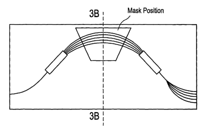
Figure 3A is a schematic top view of a preferred integrated optical waveguide
circuit phased array wavelength division multiplexer/demultiplexer device.
Also
shown is the position of the mask used for local overclad deposition.
Figure 3B shows a cross-sectional left side view of the device of Figure 3A
along dashed line AA' which comprises an uphold enabling the maslc to be held
above
the ridge.
Figure 4 shows a cross-section schematic view of a preferred waveguide with
a preferred bi-layer organic-containing overclad.
Figure SA shows a cross-section view of a preferred waveguide with a thick
glass overclad, showing the small pattern remaining at the overclad surface
above the
waveguide.
Figure SB shows a cross-section of the preferred waveguide depicted in Figure
SA after etching.
Figure SC shows a cross-section of the preferred waveguide depicted in Figure
SB after depositing a layer of an organic-containing material, thus achieving
a bi-layer
overclad.
CA 02396500 2002-07-05
WO 01/51967 PCT/US00/31256
Figure 6A and 6B show graphs of desired theoretical n(T) (index versus
temperature) curves of the organic-containing material for athermalization in
the etched
glass overclad bi-layer method, with 3 ~,m (6A) and 5 ~,m (6B) thick glass
overclad and
different n(0°C) values for the organic-containing material.
Figure 7 shows a plot of the mean channel wavelength versus temperature for
a phased array wavelength division demultiplexer device with a bi-layer
overclad of the
invention comprising an etched silicate glass pact and a polymer part
consisting of
fluorinated copolymer epoxy 16.
Figure 8 is a cross-section view of a preferred waveguide overcladded by the
thin glass overclad method of the invention.
Figure 9 shows a graph of desired theoretical n(T) (index versus temperature)
curves of the organic-containing material fox athermalization in the thin
glass overclad
bi-layer method, with a glass overclad of 0.5 p,m thiclcness and different
n(0°C) values
for the organic-containing material.
DETAILED DESCRIPTION OF PREFERRED EMBODIMENTS
The present invention comprises, in part, athermalized integrated optical
waveguide devices comprising an organic-containing overclad which inhibits the
shifting of channel wavelengths due to variations in operating temperature
within a
predetermined operating temperature range.
Integrated optical waveguide devices are well l~nown to the skilled artisan
and
are described in detail throughout the literature. Exemplary integrated
optical
waveguide devices preferably include a doped silica waveguide circuit core on
a planar
substrate, preferably a flat planar silica substrate, such as a fused silica
member, or a
silicon wafer with a silica buffer layer.
In preferred embodiments of the invention, the integrated optical waveguide
device is a phased array wavelength division multiplexer/demultiplexer with a
circuit
core having a phased array of waveguide paths. Such devices are well known to
the
skilled artisan. In some preferred embodiments of the invention, the silica
waveguide
circuit core is comprised of a first waveguide path and at least a second
waveguide path
which are preferably adjacent and substantially parallel. The present
invention,
however, encompasses a phased array of a multitude of waveguide paths, with
the
CA 02396500 2002-07-05
WO 01/51967 PCT/US00/31256
phased arrays having upwards of several hundreds of waveguide paths. In the
case of a
demultiplexer device, a wavelength multiplexed signal is inputted into the
device via an
input waveguide with the multiplexed signal comprised of multiple wavelengths
~,1, ~2,
... ~,N. A coupler region then couples the multiple wavelength signal into the
waveguide
paths of the phased array. The phased array demultiplexes (separates) the
wavelengths
7~1 through ~,N such that they are coupled through a second coupler into their
individual
channel output waveguides that exit the device. Conversely, in the case of a
phased
array multiplexes, the wavelengths 7~1 through ~,N are inputted into the
device via their
individual channel input waveguide and coupled into the waveguide paths of the
phased
, array by a first coupler region. The phased array combines the wavelengths
7~1 through
~,N such that they axe coupled through a second coupler into a common output
waveguide. In both the demultiplexer and the multiplexes devices, the phased
array
waveguide paths have a path length difference 4L that is selected to provide
an optical
path difference which corresponds to the wavelengths 7~1, ~,2, ... 7~N of the
multiplexed
signal. The optical path difference is preferably selected to correspond to
suitable
wavelengths ~,1, ~,z, ... ~,N in the range of 1500-1600 nm and to a suitable
free spectral
r ange.
The variation of mean channel wavelength with temperature in commercially
available optical devices is expressed in the following Equation l, where 7~
is the mean
channel wavelength and T the temperature:
d~,/dT = 7~ ( 1 /n x di~/dT + 1 /0L x dOL/dT) ( 1 )
Both the effective index n and the physical path length difference 0L are
temperature
dependent. The value of dn/dT is about 10-5 °C-1 for silica and can
range approximately
between - 4 x 10⁻⁴ °C-1 and - 5 x 10⁻⁵ °C-l for polymers. The
second term, "1/~L x
d~L/dT," which corresponds to the coefficient of thermal expansion of the
substrate, is
about 5.5 x 10⁻⁷ °C-1 for a silica substrate. It can be neglected in
first approximation or
can be canceled with a slightly negative dn/dT. The organic-containing
overclads of the
invention provide a negative variation of their refractive index versus
temperature. The
optical waveguide devices of the invention comprise a planar substrate
(comprising at
least a silica substrate or a silica underclad), a doped silica core, and an
overclad
comprising at least an organic-containing part, and if applicable a silicate
glass part.
CA 02396500 2002-07-05
WO 01/51967 PCT/US00/31256
The fundamental mode effective index of the optical waveguide devices of the
invention depends on the doped silica core material index (positive dn/dT), on
the silica
underclad or substrate material index (positive dn/dT), if applicable on the
silicate glass
overclad material index (positive dn/dT) and on the organic-containing
overclad
5 material index (negative dn/dT). The optical signals in the prefen~ed
devices propagate
not only in the core, but also in the clad. The organic-containing overclad
compensates
for the thermal effects (index and physical path) on the silica-containing
parts
(underclad, core, and if applicable overclad), and cancels the temperature
dependence
of the device, so that the shift of channel center wavelengths is inhibited to
less than
10 about 0.1 nm, preferably less than about 0.05 nm at temperatures in the
working range
of 0° to 70°C. Since silica presents a positive dnldT, the use
of organic-containing
overclad materials, such as polymers or sol-gels, which have negative dn/dT
values,
makes it possible to cancel the thermal deviation of channel wavelengths in a
mixed
silica-polymer system. Thus, the inventive organic-containing overclad
compositions
allow precise adjustment of the overclad index, and provide for the
athennalized
characteristics.
In preferred embodiments of the invention, the optical waveguide devices
comprise an organic-containing overclad which clads the silica waveguide
circuit core,
The organic-containing overclad preferably encapsulates the silica waveguide
circuit
core supported by a planar substrate wherein light guided by the silica
waveguide
circuit core, the organic-containing overclad, and the planar substrate
propagates in the
silica waveguide circuit core, organic-containing overclad, and planar
substrate.
In preferred embodiments of tile invention, the organic-containing overclad
has
a negative variation of refractive index versus temperature (dn/dT), and is
selected such
that the organic-containing overclad dn/dT inhibits the shift of channel
center
wavelengths to less than about 0.10 nm, preferably less than about 0.05 nm
when the
device is subjected to temperature variations in the range of 0° to
70°C. More
preferably, the organic-containing overclad and the negative variation of
refractive
index versus temperature dn/dT are selected to inhibit shifts of channel
center
wavelengths to less than about 0.01 nm.
The precise range of organic-containing overclad index useful for
athermalizing
devices depends on parameters such as core index, core dn/dT and core
dimensions. In
CA 02396500 2002-07-05
WO 01/51967 PCT/US00/31256
11
particular, the upper limit is determined by losses in curved waveguides and
depends on
the radius of curvature of waveguide circuit core. In a preferred embodiment,
the core
index is about 1.35 to 1.60, preferably about 1.40 to 1.50. More preferably
the core
index is about 1.455 ~ 0.002 at 1550 mn, 20°C, with core dn/dT assumed
to be equal to
that of silica (10-5 °C-1), and core dimensions are about 6 x 6.5 ~.m.
In this case, the
refractive index of the organic-containing overclad is in the range of 1.430
to 1.450 at
1550 nm, 20°C, most preferably between about 1.437 and about 1.447 at
1550 nm,
20°C.
Preferred organic-containing overcladdings of the invention comprise polymers
and/or copolymers containing fluorinated monomers, preferably wherein the
fluorinated
monomers are selected from the vinylic, acrylic, methacrylic or allylic
families (group
consisting of vinylics, acrylics, methacrylics and allylics). The copolymers
containing
fluorinated monomers are preferably synthesized with a free-radical process
(thermally-
induced or photo-induced). The organic-containing overclads can be comprised
of
polymers or copolymers containing other families such as fluorodioxole. If the
refractive index of the core material is higher than 1.5 at 1550 nm (with a
different
doping of the core material), new families could be used such as fluorinated
polyimides. Pentafluorostyrene (SFS), trifluoroethylmethacrylate (3FEMA),
pentadecafluorooctylacrylate (15FOA), pentafluorobenzylacrylate (SFBA), (see
Figure
1), combinations thereof, and the like are the preferred fluorinated monomers
of the
organic-containing overclads of the invention. One slcilled in the art,
however, is able
to use other fluorinated monomers, such as trifluoroethylacrylate (3FEA) or
hexafluoropropylacrylate (6FPA) (see Figure 1), in organic-containing
overclads of the
invention.
The choice of the monomers comprised in the copolymer affects not only the
refractive index but also the dn/dT of the copolymer. Typically polymers
present dn/dT
in the range of -1 x 10⁻⁴°C-1 below their temperature of glass
transition (Tg) and in the
range of -3 x 10⁻⁴°C-1 above their Tg. By changing the polymer
formulation, it is
possible to adjust the Tg, then the dn/dT. Pentafluorostyrene, methacrylates,
short side
chains (methyl or ethyl) on the monomers tend to increase the Tg of the
copolymer.
SFS, 3FEMA are preferred monomers for high Tg - less negative dn/dT
copolymers.
CA 02396500 2002-07-05
WO 01/51967 PCT/US00/31256
12
Acrylates, long side chains monomers tend to lower the Tg of the copolymer.
SFBA,
15FOA, 6FPA, are preferred monomers for low Tg - very negative dn/dT
copolymers.
Preferred organic-containing overclads are improved when a difunctional
methacrylate-epoxy monomer is added, particularly when the difunctional
methacrylate-epoxy monomer is glycidyl methacrylate (GMA) (see Figure 1).
Although not intending to be bound by theory, it is believed that the
difunctional
methacrylate-epoxy monomer provides for cationical and/or thermal cross-
linking of
the copolymers after the organic-containing overclad has been deposited over a
doped
waveguide core and planar substrate. One skilled in the art, however, is able
to use
other difunctional monomers providing for the cross-linlcing of the copolymers
of the
invention. The overclad is preferably laid from the copolymers in solution.
Typically,
the overclad is cast by spin coating, alternatively by dip-coating. The
solvent used to
dissolve and lay the copolymer of the invention may be selected from
tetrahydrofuran,
chloroform, methylene chloride, toluene and other aromatic solvents, solvents
from the
ester and the ketone families. Good results are obtained with ethyl acetate,
butyl
acetate, or butanone.
An improved polymer overclad is also obtained when using an adhesion
promoter. The preferred adhesion promoters are from the silane family. Good
results
are obtained with glycidoxypropyl trimethoxy silane (GlyMo), mercaptopropyl
trimethoxy silane (MPMo), gamma-aminopropyl trimethoxy silane (GAPS) and the
like. The adhesion promoters can be used as a surface treatment on the device
before
casting the polymer overclad. Alternatively, the adhesion promoter can be
mixed to the
solution of the polymer of the invention used to coat the device and form the
overclad.
A preferred organic-containing cladding of the invention comprises about 25-65
wt.% of trifluoroethylmethacrylate (3FEMA), about 10-75 wt.% of
pentafluorostyrene
(SFS) and about 0-30 wt.% of glycidyl methacrylate (GMA). The monomer mixture
is
preferably polymerized via free-radical process. A preferred free-radical
initiator is
about 0.1-5 wt.% 4,4'-azobis (4-cyanovaleric acid) (ADVN) overall monomer
concentration. The polymerization is preferably run in solution. In a
preferred
embodiment, the polymerization mixture is comprised of 50-95 wt.%
tetrahydrofuran
(THF).
CA 02396500 2002-07-05
WO 01/51967 PCT/US00/31256
13
Another preferred organic-containing cladding of the invention comprises about
30-80 wt.% of pentafluorostyrene (5FS), about 20-40 wt.% of
pentadecafluorooctylacrylate (15FOA) and about 0-30 wt.% of glycidyl
methacrylate
(GMA). The monomer mixture is preferably polymerized via free-radical process.
A
preferred free-radical initiator is about 0.1-5 wt.% 4,4'-azobis(4-
cyanovaleric acid)
(ADVN) overall monomer concentration. The polymerization is preferably run in
solution. In a preferred embodiment, the polymerization mixture is comprised
of 50-95
wt.% tetrahydrofuran (THF).
In preferred embodiments of the invention, the organic-containing overcladding
comprises a copolymer referred to herein as "Copolymer epoxy 9". Copolymer
epoxy 9
is prepared by polymerizing about 60 wt.% SFS, about 30 wt.% 3FEMA, and about
10
wt.% GMA. 1 wt.% of ADVN free radical initiator is added to the mixture which
is
dissolved in THF. The overall concentration of monomer in THF is usually in
the range
5-50 wt.%. The solution is stirred and warmed at 70°C for 16 hours. The
copolymer is
then isolated and purified by precipitation in methanol. The copolymer
refractive index
n at 1550 nm, 20°C is 1.447, as measured with a m-line prism coupler,
and the dn/dT is
about -1 x 10'4 °C-1, as measured by the backreflectance technique.
In other preferred embodiments of the invention, the organic-containing
overcladding comprises a copolymer referred to herein as "Copolymer epoxy 16".
Copolymer epoxy 16 is prepared by polymerizing about 67 wt.% SFS, about 29
wt.%
15FOA, and about 4 wt.% GMA. 1 wt.% of ADVN free radical initiator is added to
the
mixture which is dissolved in THF. The overall concentration of monomer in THF
is
usually in the range 5-50 wt.%. The solution is stirred and warmed at
70°C for 16
hours. The copolymer is then isolated and purified by precipitation in
methanol. The
copolymer refractive index n at 1550 nm, 20°C is ca. 1.44, and the
dn/dT at 1550 nm is
-1.4 x 10⁻⁴ °C-1, as measured using the baclcreflectance technique.
Another preferred organic-containing cladding of the invention comprises about
45-100 wt.% of pentafluorobenzylacrylate (SFBA), about 0-25 wt.% of
pentadecafluorooctylacrylate (15FOA) and about 0-30 wt.% of glycidyl
methacrylate
(GMA). Typically, the dn/dT of a copolymer prepared by polymerizing 60 wt.%
SFBA,
wt.% 15FOA, and 5 wt.% GMA, is about -3 x I O-4 °C-1.
CA 02396500 2002-07-05
WO 01/51967 PCT/US00/31256
14
In another preferred embodiment of the invention, a sol-gel overclad,
preferably
a hybrid sol-gel material, is employed as the organic-containing overclad
rather than a
polymer. A unique capability of the hybrid sol-gel materials is that the dn/dT
can be
continuously tuned by varying the composition from pure Si02 to R-SiO2i3,
where R is
an organic side group. The most significant change in this composition range
is the
average network coordination number, which for silica is 4 and for the
silsesquioxane is
3. The addition of one network coordinate bond increases the compaction and
stiffness
of the matrix, and is the primary factor that differentiates physical
properties. One
physical property that affects the index of refraction is the coefficient of
thermal
expansion, through the molar volumetric refractivity. It has been recognized
that the
dn/dT scales with the CTE. Therefore, compositional approaches can be
developed to
tune the dn/dT by using average network coordination to affect the CTE of the
material.
Pure Si02 has an expansion of 5.5 x 10⁻⁷/°C, whereas R-
SiOZi3compounds have
expansions in the 200 x 10-6/°C range. Incorporation of four-fold
coordinate silica into
three-fold coordinate hybrid shifts the expansion to significantly lower
values and
therefore shifts the dn/dT towards +1 x 10⁻⁵/°C (the value for silica)
from -3 x 10⁻⁴/°C
(the value for silsesquioxanes). A nearly linear relationship of CTE with the
average
network coordination number in a composition has been measured. Similarly, the
value
of dn/dT can be assumed to depend on the Si02 content of the hybrid material.
A
desired value of dn/dT can be made by appropriately balancing the three and
four-fold
coordinate silicon atom content in the composition. The organic sidegroups R
can be
chosen to set the index of refraction, and to slightly modify the dn/dT. To
make a
hybrid sol-gel material with dn/dT of -1 x 10-41°C, a composition with
60% Si02 and
40% R-Si02~3 is needed. To further refine the composition so that an index of
1.444 is
achieved, the 40% three-fold coordinate silicon may be comprised of 75%
ethylsilsesquioxane, and 25% phenyl silsesquioxane. Precursors with other
organic
sidechains may be used, and their effect on the index may require independent
optimization. A typical formulation for the above-mentioned hybrid material
with
di~/dT = -1 x 10⁻⁴/°C, and n = 1.444 is provided below. Briefly, 40.4
cc of TEOS is
diluted with 60 cc IPA and is reacted with between 1.5 and 2.0 cc HZO and 0.28
cc
HN03. The reaction is allowed to proceed for 60 minutes at 45°C before
addition of
CA 02396500 2002-07-05
WO 01/51967 PCT/US00/31256
between 1.5 and 2.0 cc H20. After an additional 30 minutes of reaction at
45°C, 0.9 cc
of PDMS, 17.4 cc of ETMS, and 6.4 cc of PTES are added. Finally, between 3.8
and
4.5 cc of HZO are added and reacted for 30 minutes before cooling. Prior to
use, the sol
is distilled to 50% of its volume to afford a water clear sol. The choice of
water content
5 primarily affects the cure rate properties of the rriaterial, faster rates
being achieved with
higher water content.
The mechanism used for tuning the dn/dT is to compositionally change the
average network connectivity of the silicon atoms. The silica component of the
hybrid
is supplied by the tetraethoxysila.ne precursor and the silsesquioxane
component by
10 allcoxyorganosilanes. Since both react via hydrolysis and condensation
reactions, the
mixture of the three- and four-fold coordinate silicon atoms in the final
product is
expected to be microscopically homogeneous. Therefore, properties such as the
index
of refraction are expected to be uniform over sub-micron distances in the
optical path,
which is critical for retention of acceptable performance in optical circuits.
15 The sol-gel based compositions of the invention possess low optical loss, a
means of controlling the index of refraction, and a negative shift of the
index of
refraction with increased temperature. The compositions of the invention
include, but
are not limited to, those compositions recited in WO 98/26315, WO 98/25862,
and U.S.
Provisional Application No. 60/1 I 8,946 filed February 5, 1999 of S. Dawes
and R.
Hagerty, each of which is incorporated herein by reference in its entirety.
These
compositions are particularly suitable in the present invention because of the
low
optical loss at 1550 nm, good thermal durability, good resistance to damp heat
environments, ability to tailor index of refraction compositionally, and
negative thermal
coefficient of index of refraction (dn/dT).
The dn/dT value of a composition comprising molar fractions of about 8%
polydimethylsiloxane, about 68% methyltriethoxysilane, about 8%
phenyltrifluorosilane, and about 16% phenyltriethoxysilane was measured in a
ball
termed baclcreflectance apparatus. A cleaved end of a fiber was dipped into a
sol
precursor, and cured to 250°C. The sol-gel ball term served to scatter
all transmitted
light. A standard backreflectance measurement then provided information on the
reflected light from the fiber/sol-gel interface. The ball termed fiber was
placed into an
oven along with an independent thermocouple, and reflectance measurements
acquired
CA 02396500 2002-07-05
WO 01/51967 PCT/US00/31256
16
at several temperatures between 20°C and 100°C. The value of the
index can be
calculated from the reflectance using the equation: R = (n2-nl)/(n2+nl). A
substantially
linear temperature dependence of the index was found, and the value of the
dn/dT was
established as -3 x 10-ø/°C. This value is both opposite in sign and
much higher in
magnitude than the dn/dT of silica. The magnitude of the negative dn/dT is
explained
by the high thermal expansion coefficient (200 x 10-6/°C) of the cured
hybrid sol-gel
materials. The rapid change in volume reduces the molar refractivity of the
material
and induces a negative change in the index.
To demonstrate that organic-containing materials can be used to effect a
change
in the d~,/dT properties of a phasar, a preferred device was prepared as
follows. A silica
wafer was provided with a core layer, which was etched to a desired waveguide
pattern
using standard lithography and reactive ion etch techniques widely known to
those
skilled in the art. A hybrid sol-gel overclad layer was cast onto the core
structure to
provide a 20 to 50 ~.m thick layer. The index of refraction of the sol-gel
layer was
1.447 at 1550 nm and 21 °C. The clad layer in such a structure carries
about 10% of the
light in a single mode. The device was trimmed on the input and output to
reveal the
waveguides and then the sample was measured. The phasar performance was
measured
at 21°C, 40°C, and 50°C. The phasar provided well-defined
signals on the output
channels, with rather high loss and adjacent channel crosstalk, and good
nonadjacent
channel crosstallc. In addition, the wavelength shift in each channel was -3.5
x 10-2/°C,
which is opposite the shift in silicate based core/clad compositions, and
roughly three to
four times greater in magnitude. Both the size and the direction of the
wavelength shift
are in rough agreement with the analysis of the dn/dT and f+/f
characteristic's of the
waveguide.
The loss in the device was 6 dB higher than would be expected in a silicate
overclad device, and the losses can arise from coating thickness non-
uniformity,
machining damage to the substrate/overclad interface, inexact index match, and
intrinsic loss of the sol-gel material. The adjacent crosstallc was affected
by bubble
flaws that were entrapped in the overclad layer in the phase array section of
the device.
The good non-adjacent crosstalk values indicate that the index homogeneity was
minimal. Despite the high expansion of the sol-gel, very low polarization
effects were
CA 02396500 2002-07-05
WO 01/51967 PCT/US00/31256
17
observed. The results indicate that the stresses on the system were roughly a
third less
than that in silicate systems. This result agreed with the independent stress
measurements made on films of hybrid sol-gel materials on silica. Low stresses
arise
from the low temperature process along with low modulus of the hybrid
material.
Another phased array demultiplexer was overcladded with a polymer having a
dn/dT of the order of -1 x 10⁻⁴ °C-1. The phasar was prepared by
patterning a doped
silica core layer by photolithography and reactive ion etching. The core layer
was
supported on a fused silica substrate. The core layer index (at 1550 nm) and
thickness
were 1.453 and 6.8 p,m respectively, as measured with a m-line prism coupler.
The
waveguide linewidth was found to be 6.1 p,m. The phased array device was then
overcladded with the copolymer epoxy 9 of the invention described above, by
spin-
coating a solution of 35 wt.% of copolymer epoxy 9 in 65 wt.% of ethyl acetate
on the
device.
The device overcladded with copolymer epoxy 9 was measured at 23, 53 and
71 °C. The temperature was varied by laying the device on a Peltier
element. A plot of
the mean channel wavelength versus temperature is shown in Figure 2 (solid
line with
crosses). The slope of the curve is -0.02 nm/°C, which is still
opposite in sign to the
shift in a silicate glass overcladded device (Figure 2, dotted line).
In order to further reduce the wavelength temperature dependence of the
devices, another phasar was overcladded with a polymer having a dn/dT of the
same
order as copolymer epoxy 9 (ca. -1 x 10'4 °C-1), and a smaller
refractive index at 1550
nm, 20°C. A smaller clad index induces a smaller fraction of guided
light in the clad,
and thus a smaller weight of the polymer negative dn/dT in the effective dn/dT
of the
waveguide. As previously the phasar was prepared by patterning a doped silica
core
layer supported on a silica substrate. The core layer index (at 1550 nm) and
thiclcness
were 1.453 and 6.8 pm respectively. The waveguide linewidth was found to be
6.3 p,m.
The polymer that was used to overclad this phasar device is referred to herein
as
"Copolymer epoxy 10". Copolymer epoxy 10 was prepared by polymerizing about 35
wt.% SFS, SS wt.% 3FEMA, and 10 wt.% GMA. The same procedure as for copolymer
epoxy 9 was used to prepare the copolymer and spin-coat the device. The
copolymer
layer refractive index at 1550 nm, 20°C was 1.434.
CA 02396500 2002-07-05
WO 01/51967 PCT/US00/31256
18
The device overcladded with copolymer epoxy 10 was measured at 15, 25, 50
and 70°C. A plot of the mean channel wavelength versus temperature is
shown in
Figure 2 (solid line with diamonds). These measurements show that the mean
channel
wavelength remains in a range of 0.05 nm between 15 and 70°C. Copolymer
epoxy 10
thus enables athermalization of phased array multiplexer/demultiplexer
devices.
However, the fundamental mode of waveguides overcladded with copolymer
epoxy 10 is assumed to be very asymmetrical due to the low refractive index of
this
copolymer, especially at temperatures above room temperature. As a result, the
coupling loss with a standard (SMF 28) fiber is increased by ca. 0.3 dB per
interface, as
estimated using an optical modeling software. Thus, using a copolymer with a
refractive index close to silica (at least near room temperature), such as
copolymer
epoxy.9, is desirable.
In order to compensate for the negative wavelength-temperature dependence
occuring with organic-containing overclad materials of refractive index close
to silica,
and of dn/dT values smaller than ca. -8 x 10⁻⁵ °C-1, such as copolymer
epoxy 9 or the
hybrid sol-gel material described above, the organic-containing overclad
material may
be associated to a silicate glass material with positive dn/dT, as described
hereafter.
Different patterns of organic-containing overclad are within the present
invention and include local overclad, bi-layer overclad, and hybrid overclad.
Local
overclad is characterized by local deposition of a silica clad on a portion of
the device
followed by a coating with organic-containing overclad on the remainder of the
device.
Bi-layer overclad is characterized by a bilayer made of a first layer of
silica and a
second layer of organic-containing overclad material. Hybrid overclad is
characterized
by a clad made of silica nano-particles embedded in a polymer matrix. The term
organic-containing material more particularly describes polymers and hybrid
organic/inorganic sol-gels.
Local Ovef°clad
In the local overclad method, a glass overclad is deposited only locally on
the
waveguides as shown in Figure 3A, in order to provide the organic-containing
material
~in a limited region of the overclad. More light can be exposed to the organic-
containing
region, over a shorter length. This can be accomplished by masking the region
during
CA 02396500 2002-07-05
WO 01/51967 PCT/US00/31256
19
deposition of the glass overclad. The mask, which can be a thin silica sheet,
can be held
above the waveguides by means of upholds, as shown in Figure 3B. If the sheet
is thin
enough, it can be cut far from the waveguides and removed after glass overclad
deposition. The portion of the device that was masked during glass overclad
deposition
is then overcladded with the organic-containing material.
The position of the edges of the silica sheet that cross the waveguides must
be
precisely determined in order to obtain a constant path length difference in
the glass
overcladded region ~Lg, and a constant path length difference in the organic-
containing
overcladded region ~Lp with OLg + OLp = 0L. The mean channel wavelength 7~o is
now
I O determined by m x 7~0= ng x dLg + np x 4Lp, where ng is the effective
index of glass
overcladded waveguides and np is the effective index of organic-containing
overcladded
waveguides. In order to obtain an athermalized device, the ratio of OLp to OLg
preferably equals in first approximation (neglecting the CTE term) the ratio
of dng/dT to
-dnp/dT. An advantage of the local overclad method is that near the edges of
the
device, the overclad can comprise glass. Thus, standard pigtailing techniques
(used for
full glass devices) can be employed to connect the input and output waveguides
with
the fibers that carry the optical signal.
Bi-Layer Ove~clad
In another embodiment of the invention, the organic-containing overclad is
applied using the bi-layer method. In this method, a glass overclad layer and
an
orgaaiic-containing overclad layer are superimposed as shown schematically in
Figure
4. The configuration is tailored so that only the desired fraction of light
passes through
the negative dn/dT region to balance the effective index of refraction
according to
Equation II : f x (dn-/dT) = f+ x (dn+/dT), where the fraction in the negative
dn-/dT
material is indicated by f and the fraction in the positive do+/dT materials
is indicated
by f+. Preferably, a bi-layer overclad can be applied in two different
manners: etched
glass overclad and thin glass overclad.
In the etched glass overclad method, a thick glass overclad is first deposited
on
the waveguides. Typically, a small pattern remains at the overclad surface
along the
waveguides (see Figure SA). Then the glass overclad is etched until reaching
the top
side of the waveguide core (see Figure SB). An optional lithography masking
method
CA 02396500 2002-07-05
WO 01/51967 PCT/US00/31256
can be used to etch the device in the phased array region only, for easier
pigtailing at
the device input/outputs. Since only etching is needed to remove overclad, no
highly
precise patterning is needed. The device is then overcladded with an overclad
material
of the invention.
5 The effective index of such waveguides with the approximate shape of Figure
4
has been calculated using optical modeling software. The following sets of
parameters
were used:
wavelength: 1550 nm
core width and height: 6 ~,m x 6.5 ~,m
10 silica CTE: 5.5 x 10'7°C'1
silica substrate and glass overclad indices at 0°C: 1.444
core index at 0°C: 1.455 (corresponding to a D of 0.75%)
silica substrate, glass overclad and core dn/dT's: 10.5 x 10'6°C'i
(assumed to be
equal to silica dn/dT in the visible range)
15 organic-containing overclad index at 0°C: 1.443, 1.444, or 1.445
glass overclad thickness remaining on both sides of the waveguides after
etching: 3 ~,m or S~,m.
For each of the six sets of parameters (corresponding to different organic-
containing material indices and glass overclad thiclcnesses), the effective
index at 0°C
20 was first calculated. Then at higher temperatures T (from I O to
70°C by steps of 10°C)
the effective index ne~(T) desired for athermalization was calculated using
Equation 1
and the organic-containing material index desired to obtain the effective
index ne~{T)
was calculated with commercially available optical modeling software. The
results are
shown in Figure 6A (3 ~,m thick glass overclad) and 6B (5 ~.m thick glass
overclad).
Figures 6A and 6B show that the dn/dT of the organic-containing material
preferably
becomes more negative at higher temperatures, which is the case for utilized
polymers.
The average dn/dT between 0 and 70°C is preferably about (-1.8 ~ 0.2) x
10'4°C'I in
the case of 3 ~m thick glass overclad and preferably about (-3.3 ~ 0.2) x
10'4°C'1 in the
case of 5 ~,m thick glass overclad. An advantage of the present method is that
pigtailing
is facilitated because the edges of the device are overcladded with glass.
CA 02396500 2002-07-05
WO 01/51967 PCT/US00/31256
21
A phased array demultiplexer was overcladded using the etched glass overclad
method. The phasar was prepared by patterning a doped silica core layer by
photolithography and reactive ion etching. The core layer was supported on a
fused
silica substrate. A glass overclad was then deposited by flame hydrolysis
deposition,
S consolidated at 1240°C for 3/4 hr and then partially etched away,
leaving about 2 ~,m of
overclad above the waveguides. The phased array device was then overcladded
with the
copolymer epoxy 16 (described above) by spin-coating a solution of 3S wt.% of
copolymer epoxy 16 in 6S wt.% of ethyl acetate on the device.
The device overcladded with copolymer epoxy 16 was measured at 15, 23, S0,
70 and 80°C. A plot of the mean channel wavelength versus temperature
is shown in
Figure 7. The slope of the curve is + 0.007 nml°C, which is slightly
smaller than the
shift in a silicate glass overcladded device (+ 0.01 nm/°C). A greater
impact of the
negative dn/dT overclad would have been achieved if the glass overclad had
been more
deeply etched away.
1 S In another embodiment of the invention, a second bi-layer method can be
employed. The thin glass overclad method comprises first depositing a very
thin glass
overclad layer on a device followed by overcladding with a negative dn/dT
organic-
containing material. A cross-section of such a waveguide is depicted in Figure
8.
Theoretical n(T) curves were calculated as described above for the etched
glass
overclad method. Curves for a glass overclad thickness of 0.5 ~,m are shown in
Figure
9. The dn/dT of the organic-containing material becomes more negative at
higher
temperatures. The average dn/dT between 0 and 70°C is preferably about
(-3.0 ~ 0.4) x
10-4°C-1 for the glass overclad thickness of 0.5 ~,m. An advantage of
the present method
is the manufacturability and economical approach of the procedure. In
addition, the
ZS thiclcness of the glass overclad can be easily tuned to adjust the channel
wavelength
shift to zero. In a preferred embodiment, an optimal glass overclad thickness
(tuned
thickness) for the device core waveguide and -dn/dT organic containing
overclad is
determined to minimize channel wavelength shift. The device is then provided
with
such a tuned glass overclad thickness which inhibits channel wavelength shift.
Hybrid Ove~clad
In another preferred embodiment of the invention, the hybrid overclad method
is
employed. In the hybrid method, the overclad is preferably made by mixing a
polymer
CA 02396500 2002-07-05
WO 01/51967 PCT/US00/31256
22
overclad material with silica nano-particles. The mixture of the negative
dn/dT
polymer with positive cli~/dT silica provides a material with a less negative
dn/dT,
suitable for overcladding the device of the invention. The presence of epoxy
groups in
the polymer and the use of an adhesion promoter such as, for example,
glycidoxypropyl
trimethoxysilane or mercaptopropyl trimethoxysilane, or the like, provides
compatibility between the glass and polymer and provides good dispersion of
the silica
particles with no phase separation. Silica nano-particles with diameters
smaller than 10
nm are preferred and are commercially available. The hybrid material
polymer/silica
nano-particles is transparent in the visible-near IR range and the domains of
different
index are preferably too small to increase the propagation losses at 1.55 ~,m.
It will be apparent to those skilled in the art that various modifications and
variations can be made in the methods, compositions, and devices of the
present
invention without departing from the spirit or scope of the invention. Thus,
it is
intended that the present invention covers the modifications and variations of
this
invention provided they come within the scope of the appended claims and their
equivalents.