Note: Descriptions are shown in the official language in which they were submitted.
CA 02396570 2002-07-05
WO 01/51276 PCT/USO1/00366
-1-
FABRICATION OF METALLIC MICROSTRUCTURES VIA EXPOSURE OF
PHOTOSENSITIVE COMPOSITION
RELATED APPLICATIONS
This application claims priority to U.S. Provisional Patent Application Serial
No.
60/175,068, filed January 7, 2000.
STATEMENT AS TO POTENTIAL RIGHTS UNDER FEDERALLY
SPONSORED RESEARCH AND DEVELOPMENT
to Research leading to the invention disclosed and claimed herein was
supported by
DARPA and the National Science Foundation (NSF) (ECS-9729405). This work used
MRSEC shared facilities supported by the NSF (DMR-9400396 and DMR-9809363).
'The U.S. Government may have certain rights to the invention.
1s ' FIELD OF THE INVENTION
This invention relates to methods for forming a conductive pattern using
photographic film.
BACKGROUND OF THE INVENTION
2o A multitude of techniques for shaping (such as stamping, grinding, and
milling) and joining (such as welding and mechanical joining) metals are
highly
developed for the fabrication of macroscopic structures. Application of these
techniques
to the fabrication and assembly of metallic microstructures (structures having
features
<100 ~,m) becomes increasingly difficult as the feature sizes become smaller.
For that
25 reason, new approaches to microfabrication that are not derived from
fabrication
techniques used on a large scale have been developed. A widely used technique
for
fabrication of metallic microstructures is microelectrodeposition of metals on
an
appropriately shaped mandrel or template. Two examples of this class of
processes are
through-mask electroplating and LIGA (Lithographie, Galvanoformung,
Abformung),
3o both of which are based on projection photolithography (for LIGA, commonly
carried
out using x-rays, although the availability of the SU-8 class of photoresist
has reduced
the need for x-ray exposure in making thick structures). Although these
methods provide
ways to form metallic microstructures, they axe processes with several steps,
and require
facilities of limited availability.
CA 02396570 2002-07-05
WO 01/51276 PCT/USO1/00366
-2-
Recently, methods for the microfabrication of metallic, 2D and 3D structures
based on the combination of soft lithography and microelectrodeposition have
been
described, the latter both through a mask of photoresist and onto patterned,
conducting
surfaces. The pattern-transfer step in these soft lithographic techniques
typically uses an
elastomeric stamp with a surface relief structure that carries the desired
pattern. These
stamps are usually formed by molding polydimethylsiloxane (PDMS) against a
'master'
composed of a relief pattern in photoresist, and obtained by photolithography.
These
masters may be generated using a technique based on high-resolution commercial
printing and high-resolution optical reduction. This procedure is efficient:
from design,
to through stamp, to initial structure typically requires no more than 24
hours. Both the
preparation of the mask and the generation of the master by photolithography
may
require access to specialized devices and facilities (i.e., high-resolution
image setters,
clean rooms) that are more readily available than the mask-making facilities
required in
high-resolution photolithography, but that are still not available to every
laboratory that
might benefit from medium resolution microfabrication.
SUMMARY OF THE INVENTION
The present invention provides a method for producing metallic and other
conductive microstructures. The microstructures may be produced on a
substrate, for
example, a planar substrate such as photographic film, and may subsequently be
removed from the substrate. The microstructures may be produced in a short
amount of
time and may use equipment readily available to those skilled in the axt.
In one aspect, a method is provided in which a conductive pattern is formed.
An
article including a metal atom precursor capable of conversion to elemental
metal is
provided and a first portion of the article is disproportionately exposed to
electromagnetic radiation at a level greater than at a second portion of the
article. The
article is exposed in an amount and for a period of time sufficient to convert
at least
some of the precursor at one of the portions to elemental metal at a
conversion level
greater than conversion of precursor to elemental metal at the other portion.
Then, a
3o metal is deposited from a source external of the metal atom precursor,
proximate the
portion of the article including metal atom precursor converted at a greater
conversion
level in an amount greater than deposition of metal at the other portion.
CA 02396570 2002-07-05
WO 01/51276 PCT/USO1/00366
-3-
In another aspect, the invention provides for a method that includes deforming
a
flexible metal structure from a first configuration to a second configuration
and
depositing auxiliary metal on the metal structure to the extent that the
structure is self
supporting in the second configuration.
In another aspect, the invention provides for a method that includes exposing
photoresist to electromagnetic radiation through a metal mask, developing the
photoresist
to form a photoresist pattern, directing a metal deposition composition to the
metal mask
via the photoresist pattern, and depositing auxiliary metal on the metal mask.
In another aspect, the invention provides for a method of forming a conductive
to pattern. A photographic film is illuminated with a desired illumination
configuration, and
the film is developed so that illuminated or non-illuminated portions of the
film are
adjusted to be in an altered state. Additional conductive material is
selectively deposited
onto portions of the film in an altered state in amounts greater than amounts
of
conductive material deposited on portions of the film not in the altered
state.
In another aspect, the invention provides for a method of forming a
discontinuous
metallic structure. A photographic film is illuminated with a desired
structure
configuration and the film is developed so that illuminated or non-illuminated
portions of
the film are adjusted to be in an altered state. Additional conductive
material is
selectively deposited onto portions of the film in an altered state in amounts
greater than
2o amounts of conductive material deposited on portions of the film not in the
altered state.
Other advantages, novel features, and objects of the invention will become
apparent from the following detailed description of the invention when
considered in
conjunction with the accompanying drawings, which are schematic and which are
not
intended to be drawn to scale. In the figures, each identical or neaxly
identical
component that is illustrated in various figures is represented by a single
numeral. For
purposes of clarity, not every component is labeled in every figure, nor is
every
component of each embodiment of the invention shown where illustration is not
necessary to allow those of ordinary skill in the art to understand the
invention.
3o BRIEF DESCRIPTION OF THE DRAWINGS
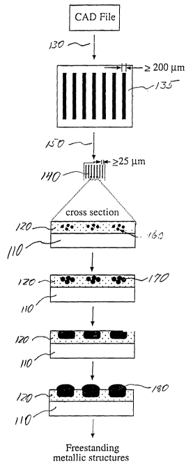
Figure 1 provides a schematic flow chart illustrating one embodiment of the
invention.
CA 02396570 2002-07-05
WO 01/51276 PCT/USO1/00366
-4-
Figure 2 provides a photocopy of three optical micrographs (a, b and c)
showing
three successive stages in the production of a microstructure developed using
an
embodiment of the invention. Each of Figures 2a, 2b and 2c also includes a
photocopy of
a micrograph of each stage at greater magnification.
Figure 3a provides a photocopy of an optical micrograph showing a serpentine
gold wire produced using an embodiment of the invention as well as an oblique
view of
the edge of the same wire.
Figure 3b provides a graph providing results for electrical resistance at
different
contact points along the gold wire of Figure 3a.
to Figures 4a - 4c illustrate three different schematic views of a
microfluidic system
produced by an embodiment of the invention.
Figure 4a illustrates a starting design as printed on paper.
Figure 4b illustrates a three dimensional perspective view of a microfluidic
system.
15 Figure 4c provides a photocopy of an optical micrograph of the three
electrodes
of the microfluidic system of Figure 4b.
Figure 4d provides the results of a cyclic voltammogram obtained using the
microfluidic system shown in Figs. 4b and 4c.
Figures Sa-Sc provide a photocopy of three optical micrographs that
2o schematically illustrate the stepwise assembly of a three-circle open
spherical structure
using an embodiment of the invention.
Figures 6a-6b provide a schematic illustration (6a) and an optical micrograph
(6b) that illustrate the formation of a curved metallic structure from a
planar metallic
structure using an embodiment of the invention.
25 Figures 7a-7c provide a photocopy of three optical micrographs illustrating
the
formation of discontinuous metallic structures on a single substrate.
Figure 8a provides a schematic illustration of an embodiment of the invention
used to produce a free standing metallic structure.
Figure 8b provides a photocopy of an optical micrograph of a metallic
structure
3o produced by the method illustrated in Figure 8a.
CA 02396570 2002-07-05
WO 01/51276 PCT/USO1/00366
-5-
DETAILED DESCRIPTION
The invention provides a method for forming a pattern of conductive material
on
a planar or non-planar substrate. The substrate may include a chemical
composition that
can be altered by illumination with electromagnetic radiation. The substrate
may be
flexible or rigid. Preferably, the substrate includes a photosensitive
composition, such
as that included in a photographic or other photosensitive film. The
photosensitive
composition can include any type of photosensitive composition having suitable
properties, such as a metal atom precursor or other material that changes
state in
response to exposure (or non-exposure) to electromagnetic radiation and
possible
1o subsequent development, and facilitates subsequent selective deposition of
a conductive
material onto or away from material areas experiencing the state change.
Imone aspect of the invention, a photographic film is exposed to an
illumination
configuration having a desired pattern. For example, the photographic film can
be
standaxd black and white or color 35 mm photographic negative film, black and
white or
color slide (i.e., positive) film, laxge format photographic film, instant
black and white or
color film, black and white or color print paper, etc. The photographic film
may be
exposed to the illumination configuration in various ways, including using the
film in a
standard photographic camera to image a desired pattern, directing a beam or
multiple
beams of illumination, e.g., a laser beam, to illuminate desired portions of
the
2o photographic film, placing the film in sufficiently close proximity to a
display device
(such as a CRT display, electroluminescent (EL) display, a back-lit LCD, etc.)
that
displays a desired pattern and therefore illuminates the photographic film
with the
desired pattern, etc. Thus, desired portions of the photographic film can be
disproportionately exposed to electromagnetic radiation at a level greater
than other
portions of the film. When exposing the photographic film using a standard
photographic camera, the film can image a printed haxd copy of a pattern, such
as a
circuit pattern printed or drawn onto a paper substrate, for example, by a
computer-aided
design (CAD) application and associated printer, or the film can image an
actual sample
of the pattern, such as an actual circuit boaxd pattern. When exposing the
film using a
3o scanned illumination beam or other display, a CAD image file or other image
data can be
used to drive the illumination beam scanner, display or other device so that
the film is
exposed to the desired illumination configuration pattern.
CA 02396570 2002-07-05
WO 01/51276 PCT/USO1/00366
-6-
Exposing the substrate, e.g., photographic film, to the desired illumination
configuration causes illuminated or non-illuminated portions of the
photographic
composition to be adjusted into an altered state, i.e., experience a physical
or chemical
change. For example, if a photosensitive composition including a metal atom
precursor,
such as that in conventional silver halide photographic film, is used,
exposure (or non-
exposure) of the metal atom precursor to electromagnetic radiation (and
possible
subsequent development) can cause the precursor to change to an altered state,
such as an
elemental metal. Thus, if conventional silver halide photographic slide film
is exposed
to a desired illumination configuration, relatively darker or non-illuminated
portions of
1o the film will experience a chemical change such that silver particles
(elemental silver), or
grains, are formed in a lugher density at low-level or non-illuminated
portions of the film
compared to film portions exposed to a higher level of illumination. In most
photographic films, the physical or chemical change results after the film is
exposed to
illumination and developed using conventional development techniques. However,
the
physical or chemical change in the illuminated or non-illuminated film
portions can
occur simultaneously with exposure or shortly thereafter without requiring
conventional
photographic development. For example, when using instant photographic films,
development occurs shortly after the film is exposed to illumination and does
not require
an additional development step. Both the exposure time and the illumination
intensity
2o are typically equal to those used in standard photographic processes and
are known to
those skilled in the art. When substrates other than photographic film are
used, exposure
times and illumination intensities can be routinely determined.
After the substrate is exposed to an illumination configuration, the
illuminated or
non-illuminated portions may be augmented, or further developed, by depositing
a metal
or other conductive material selectively on the illuminated or non-illuminated
portions
(portions experiencing or not experiencing a state change). For example, when
using
conventional silver halide photographic slide film, non-illuminated portions
of the
developed film can be further augmented using an electroless deposition of
elemental
silver such that the deposited silver is catalyzed by the silver grains in the
photographic
3o film to selectively increase the silver grain size in the film at the non-
illuminated
portions. Thus, further development or augmenting of the film can result in an
electrically continuous pattern in portions of the film, i.e., individual
silver grains in the
CA 02396570 2002-07-05
WO 01/51276 PCT/USO1/00366
_7_
film are selectively grown so that the grains in illuminated or non-
illuminated portions
contact each other or otherwise interact so as to form an electrically
conductive structure
on the portion. A metal is deposited in an amount sufficient to provide
conductivity to a
portion when the portion on which the metal is deposited becomes conductive
between
one end of the portion and an opposing end of the portion. Once a portion of
the film
becomes conductive, this portion of the film can be additionally plated, for
example by
using electrochemical deposition of a metal or other conductive material onto
the
augmented film portions. This additional deposition step can increase the
width and/or
thickness of the augmented portions, if desired. The result may be an
electrically
1o conductive pattern that matches, or neaxly matches, the pattern of the
illumination
configuration used to expose the photographic film. The electrically
conductive pattern
can be used for testing, prototyping, actual field use, for use as a mask in
photolithographic processing, etc.
As described below in one example of the invention, a pattern of silver
particles
embedded in the gelatin matrix of exposed and developed silver halide-based
photographic film can serve as a template in a broadly applicable method for
the
microfabrication of metallic structures or microstructures. In this exemplary
method, a
CAD file or portion of a CAD file is reproduced, or approximately reproduced,
in the
photographic film by exposure and developing. In this example, the resulting
pattern of
2o discontinuous silver grains is developed, i.e., augmented and made
electrically
continuous, by electroless deposition of silver, and the electrically
continuous structure is
then used as the cathode for electrochemical deposition of an additional layer
of the same
or different metal or other conductive material. The overall process can be
completed
witlun 2 hours, starting from a CAD file, and can generate structures with the
smallest
dimension in the plane of the film of ~30 Vim. Structures with an aspect ratio
of up to
five can also be obtained by using the metallic structures as photomasks in
photolithography using a photo resist, such as SU-8 photoresist, on the top of
the
electroplated pattern, and exposed from the bottom, followed by development
and
electroplating through the patterned photoresist. This method of fabrication
uses readily
3o available equipment, and makes it possible to prototype a wide variety of
metallic
structures and devices. The resulting structures -- either supported on the
film backing,
or freed from it and possibly mounted on another substrate -- axe appropriate
for use as
CA 02396570 2002-07-05
WO 01/51276 PCT/USO1/00366
_g_
passive, structural materials such as wire frames or meshes, as electric
circuits and in
microfluidic, microanalytical, and microelectromechanical systems (MEMS).
The method of microfabrication described below enables rapid prototyping of
metallic microstructures with planar dimensions >_30 Vim. A single, continuous
structure
or two or more discontinuous structures may be produced on a single substrate.
Production of discontinuous structures may, therefore, be performed
simultaneously. An
advantage of the described procedure is that laboratories with no access to
sophisticated
facilities for writing the masks required for photolithography can carry out
microfabrication at feature sizes useful in a range of applications such as,
for example:
to microfluidic systems, cell biology, microanalytical systems, microsensor,
and
microelectromechanical systems (MEMS).
One example of a pattern fabrication process involves five steps: i) printing
of a
design embedded in a CAD file on paper using a high-quality (e.g., 600 dots
per inch, or
greater, dpi printer; ii) photographic reduction of this print onto a silver
halide-based
photographic film using a commercial slide maker; iii) development of the
exposed film;
iv) electroless deposition of silver metal directly on the exposed, developed
film - that is,
the finished slide - to make at least portions of the pattern electrically
continuous; and v)
optional electrochemical deposition of metal or other electroactive or
conductive
material onto the silver to form or reinforce the final pattern. This method
can be
2o especially useful in the fabrication of metallic microstructures for use in
prototyping
devices, and in applications -- 3D fabrication, fabrication with unfamiliar
materials --
where conventional projection photolithography is difficult to apply or
inapplicable.
One aspect of the invention uses a readily available photographic film
recorder --
a commercial slide (transparency) maker -- that reproduces the pattern of a
CAD file --
~c ...,.....+~.Pl .~... ,...",.or ~.~+1. .~".. .~~~i.o r.rir,f~nr va;ranfv<r
a"~+n oi~mr ~o~i~o_~ooo~ rWniwrrrorv'G,in
CA 02396570 2002-07-05
WO 01/51276 PCT/USO1/00366
-9-
procedure makes it possible for virtually all laboratories to generate a
variety of useful
metallic structures with small planar feature sizes, for example, 30 wm.
The single step of the simple photographic reproduction of a CAD, or other,
file
onto a silver halide-based film can replace the multiple (partly
photolithographic) steps
in microcontact printing and LIGA for the fabrication of appropriately shaped
mandrels
for microelectrodeposition. The complete procedure from CAD-file to metallic
structure
can easily be completed within two hours if instant film is used. Any photo
camera or
slide maker that accepts silver halide-based or other suitable photographic
film may be
sufficient for the reproduction of the CAD file pattern. Structures with
thickness smaller
to than 2 ~,m may be porous due to the gelatin network. Higher resolution in
the width of
the structures can be obtained using more professional photographic equipment.
It is
believed that the intrinsic limit of resolution for this technique lies with
the quality of the
photographic equipment and is limited by aberrations of the optical elements,
and not by
the size of the grains in the film (<100 nm). The maximum size of a structure -
- or an
array of structures -- is limited by the size of the film used, typically 35
mm x 22 mm.
Larger size silver halide-based film is available (up to 300 mm x 400 mm).
The following describes a specific, exemplary method of the invention and
experimental results. However, as discussed above, the invention is not
limited to this
specific example in which a desired pattern is first printed using a computer-
drawing
(CAD) and the printed pattern is imaged onto a silver halide photographic
film. Rather,
other types of substrates, such as photographic films, imaging methods and/or
conductive
material augmentation processes can be used. For example, an actual micro
circuit
device could be used to image a frame of photographic film, i.e., one could
"take a
picture" of an actual microcircuit device and use the imaged photographic film
to prepare
a conductive circuit pattern by developing the film using conventional
photographic
techniques and further developing or augmenting the film using electroless
plating,
electro plating, or other selective deposition of conductive materials onto
desired
portions of the film.
3 o EXAMPLES
Polagraph 35 mm instant black and white slide film (Polaroid Corporation;
Cambridge, MA) was used as an article presenting metal atom precursors. Halo-
CA 02396570 2002-07-05
WO 01/51276 PCT/USO1/00366
-10-
ChromeTM silver electroless plating solution (Rockland Colloid Corp; Piermont,
NY),
Tech 25 E gold plating solution (Technic Inc.; Providence, R. L), Tech nickel
plating
solution (Technic Inc.; Providence, R. L), Polydimethylsiloxane (Sylgard 184;
Dow
Corning, N.Y.), and SU-8 photoresist (Microchem Co.; Newton, MA) were used as
received. NiS04~6H20 (99%), NH3~H20 (29.8%), Na2HaPOa~H20 (>99%), Ru(NH3)6C13
(>99%), NaCI (>99%), HCl (1N), Na2S2O3 (>99%), K3Fe(CN)6 (>99%), K4Fe(CN)6
(99%), and propylene glycol methyl ether acetate (PGMEA) were obtained from
Aldrich.
A black and white slide maker was bought from Polaroid (Model IPC-2). The
scanning
electron micrograph (SEM) was done on a LEO digital scanning electron
microscope,
to model 982 and the cyclic voltammetry measurements were performed on a AFCB1
Bipotentiostat (Pine Instrument Company; Grove City, PA).
Test patterns were designed using FreehandTM software (Adobe Systems Inc.)
and printed on paper using a 600 dpi printer. The printed images were reduced
in size on
slide films using the black and white slide maker. The contrast was set in the
medium
contrast mode and the exposure time was ~0.5 second. The slide film was
developed
using the developing package for Polagraph 35 mm slide film. The developed
film was
put in the silver electroless plating solution for about 15 minutes, then the
desired metal
was electroplated onto the patterns of silver.
Example 1
Figure 1 illustrates an exemplary procedure used to fabricate metallic
microstructures using silver halide-based photographic film. One element in
this film is
a substrate 110, a polyester backing (typically 100 ~,m thick) covered with a
gelatin
layer 120 (typically ~2 ~m thick) that contains silver halide. (Keller, K.
Science and
Technology of Photography; VCH: Weinheim, German, 1993.) A CAD file was first
printed (130) on paper 135 with a 600 dpi office printer. A commercial slide
maker was
then used to reproduce (150) the black and white image on the silver halide-
based
photographic film 140. The initially developed film leaves the silver
particles 160
isolated, with no electrically continuous path connecting adjacent portions in
the pattern.
3o Electroless deposition of additional silver, catalyzed by these silver
grains, increased the
grain size so that the grains come into contact 170. (Bjelkhagen, H.I.
SilverHalide
Recording Materials for Holography and Them Processing; Springer-Verlag: New
York,
CA 02396570 2002-07-05
WO 01/51276 PCT/USO1/00366
-11-
1995 and Zhang, Y.; Yan, T.; Yu, S.; Zhuang, S. Jou~hal of the Electrochemical
Society
1999, 146, 1270.) At that point, all portions of the pattern image become
electrically
conducting (provided, of course, that the original design was continuous).
Subsequent
electroplating using this image as the cathode provided metal structures that
had the
mechanical strength or optical density required for further applications.
Freestanding
metallic microstructures 180 can be obtained by dissolution of the gelatin
matrix in
which the metallic structures are embedded. Due to the high permeability of
the gelatin
layer (~2 ~m thick), (Bjelkhagen, H.I. SilverHalide Recording Materials fog
Holography and Their Processing; Springer-Verlag: New York, 1995,) the metal
was
to deposited from both the side and the top onto the silver structures during
the initial
electroplating process. Once the upper surface of the metal grew out of the
gelatin layer,
the speed of deposition on the top of the metal structure was higher than on
the side due
to mass transport limitations to delivering metal ions to the sides of the
structures, or
within the gelatin film.
Example 2
Figure 2 shows optical micrographs of metallic lines (~30 ~m wide) generated
by
each of the steps in the fabrication process described above in Example 1.
After
development of the photographic image and before electroless deposition (Fig.
2a), the
primary pattern of silver halide grains had a line width of ~25 ~m and an edge
roughness
of ~2 ~,m. After electroless plating (Fig. 2b), the line width increased to
~26 ~m and the
edge roughness remained approximately the same. After electroplating (Fig.
2c), a line
width of ~30 ~,m and an edge roughness of ~3 ~,m were observed. The limited
optics of
the slide maker resulted in distorted, incomplete reproduction of patterns
with smaller
features. The edge roughness of patterns printed on the paper also contributed
to the
resolution of the final pattern, but it was not the major factor. The smallest
feature sizes
of metallic structures obtained using a master pattern printed with a 3387 dpi
high-
resolution image-setter were still ~30 ~,m, with edge roughness of ~3 Vim.
Figure 2 also
shows scanning electron micrographs of the microstructure of the line patterns
in the
3o different stages of the fabrication process. The growth and fusion of
silver particles upon
electroless plating and electroplating are clearly visible.
CA 02396570 2002-07-05
WO 01/51276 PCT/USO1/00366
-12-
Example 3
Figure 3a shows a gold serpentine wire (~50 ~m wide and ~2.5 ~m thick; total
length of 648 mm) fabricated to test the electrical continuity of metallic
structures made
using this procedure as described in Example 1. A uniform resistivity of ~7 x
10-8 S2m
(Figure 3b) was measured over the full length of the wire, which is ~3.5 times
higher
than the value reported for pure bulk gold (~2 x 10'8 S2m). (Lide, D.R. CRC
Handbook of
Chemistry ahd Physics; CRC Press: New York, 1999.) A residual gelatin network,
or a
network of grain boundaries still present inside the wires after
electroplating, are possible
to explanations for this difference.
Example 4
A three-electrode system was fabricated using the procedure described above
and
is illustrated in Figure 4. Figure 4a illustrates the design of the system on
paper prior to
reducing the size of the system and transferring it to film. The electrodes
are represented
on paper by lines 410, 420 and 450, and their contact pads by structures 412,
422 and
452 (40 mm x 40 mm). The electrodes (Figs. 4b and 4c) were differentiated into
two sets
by selective electroplating: two wires, 490 and 492, and their contact pads,
494 and 496,
(5 mm x 5 mm) were covered with gold (for the working and counter electrodes,
430 and
440, respectively) and one wire 482 and corresponding contact pad 484 (5 mm x
5 mm)
with silver (for the reference electrode 460). The polyester base 474 in the
film enabled
the use of tlus three-electrode structure in a microfluidic device by placing
a
polydimethylsiloxane (PDMS) membrane 470 having an inlet 476 and an outlet 478
with
a channel 480 embossed in its surface directly on this structure (Figure 4b
and 4c). The
PDMS membrane was made by casting PDMS against an SU-8 master. (Xia, Y.;
Whitesides, G.M. Agnew. Chem. l~t. Ed. E~cgl. 1998, 37, 550.)
Cyclic voltammetry (Figure 4d) of a solution containing Ru(NH3)6C13
demonstrated the performance of this three-electrode system. The solutions
were
injected into the channel using a single-use syringe connected to the inlet
with a piece of
3o polyethylene tubing. The system was treated with a O.1N HC1 solution for
about one
minute prior to the electrochemical measurements. The concentration of oxygen
in all
solution was reduced by bubbling Ar gas through for at least 5 minutes.
CA 02396570 2002-07-05
WO 01/51276 PCT/USO1/00366
-13-
Example 5
The solubility of a gelatin base in DMF or hot water allows for the
fabrication of
freestanding structures. (Bjelkhagen, H.I. Silver-Halide Recording Materials
for
Holography and Their P~ocessihg; Springer-Verlag: New York, 1995.) The
conditions
required for release are sufficiently gentle that even fragile structures are
not damaged.
Figure 5 shows sequentially, in Figures Sa, Sb and Sc, the construction of a
3D structure,
an open sphere, assembled from pieces that have been fabricated using the
technique
described in Example 1. The line width of each of the nickel circles was ~l mm
and
1o their thickness was ~50 Vim. This example illustrates an alternative
approach to rapid
fabrication of elements for 3D structures/MEMS.
Example 6
Flexible substrates, such as photographic film, make it possible to fabricate
topologically complex microstructures. Figure 6(b) shows a nickel serpentine
wire (~2
~m thick, and 100 ~.m wide) fabricated by electroplating on a folded silver
halide film.
The film was exposed in a planar orientation (Fig. 6a) and folded prior to
electroless
deposition and subsequent electroplating.
2o Example 7
The procedure described above works well to make continuous metallic
structures. During the fabrication of discontinuous structures, there is no
continuous
electrical pathway joining all the elements of the pattern, and therefore it
is less practical
to use electroplating. An electroless Ni plating solution (2.6 g NiS04~6H20, 5
ml
NH3~H20, and 3.6 g Na2H2PO2-H20 in 200 ml H20) was used to build a thick Ni
layer on
the patterned silver particles (continuous or discontinuous). Figure 7a shows
a "Veritas"
logo consisting of a ~2 ~m nickel layer deposited using electroless plating
alone.
Figures 7b and 7c illustrate magnified portions of Figure 7a to show detail of
the
continuous individual structures obtained on a single substrate without the
use of
3o electroplating.
CA 02396570 2002-07-05
WO 01/51276 PCT/USO1/00366
- 14-
Example 8
The structures fabricated above all have relatively low aspect ratios (height
width), typically less than 0.1. Figure 8 shows a procedure for the
fabrication of
structures with a high aspect ratio. First, the film carrying the low aspect
ratio structure
was used both as the substrate and the mask in a photolithographic step. The
photoresist
810 was exposed to UV light from below the structure/mask 820 layer.
Subsequent use
of the photoresist pattern as the mask to direct electrodeposition of metals
while using
the original, low aspect ratio structure as the cathode resulted in high
aspect ratio
structures. The high aspect structures were produced as follows:
to Electroplated film was produced as outlined above. The electroplated film
was
put in an etching solution containing 0.1 M Na2Sa03/0.01 M K3Fe(CN)6/0.001 M
K4Fe(CN)6 for ~1 min to remove the gold particles reduced by the gelatin in
the non-
patterned area. This etching step is preferred to make the film more
transparent to UV
during the patterning of photoresist. The film was immobilized on a glass
slide using
cellophane tape. SU-8 photoresist was spincoated directly onto the film at 500
rpm for 20
s. The film was baked at 95 °C for ~10 hours, followed by exposure from
the bottom for
7.5 min (10 mJ~cm 2~S-1 at 405 nm) with a Karl Zeiss MJB3 contact aligner and
post-
baking at 90 °C for ~10 min. The photoresist was developed in PGMEA for
~4 hours
with magnetic stirring. Finally, through mask electroplating of the film
carrying the
patterned photoresist in a nickel electroplating bath was performed for 150
hours while
maintaining a current of 10 mA.
The fact that the film served as the substrate and the fact that the metallic
structures on the film not only served as the mask in the photolithographic
step, but also
as the cathode in the electroplating procedure reduce the number of steps
significantly
compared to conventional processes for the fabrication of high aspect ratio
metallic
structures. We obtained a negative Poisson ratio structure (Xu, B.; Arias, F.;
Brittain,
S.T.; Zhao, X.-M.; Grzybowski, B.; Torquato, S.; Whitesides, G.M. Adv Mater.
in press
1999) with a maximum aspect ratio of 5 (Figure 8b).
Those skilled in the art would readily appreciate that all parameters and
3o configurations described herein are meant to be exemplary and that actual
parameters
and configurations will depend upon the specific application for which the
systems and
methods of the present invention are used. Those skilled in the art will
recognize, or be
CA 02396570 2002-07-05
WO 01/51276 PCT/USO1/00366
-15-
able to ascertain using no more than routine experimentation, many equivalents
to the
specific embodiments of the invention described herein. It is, therefore, to
be understood
that the foregoing embodiments are presented by way of example only and that,
within
the scope of the appended claims and equivalents thereto, the invention may be
practiced
otherwise than as specifically described. The present invention is directed to
each
individual feature, system, or method described herein. In addition, any
combination of
two or more such features, systems or methods, provided that such features,
systems, or
methods are not mutually inconsistent, is included within the scope of the
present
invention.
to