Note: Descriptions are shown in the official language in which they were submitted.
CA 02397278 2002-08-09
W1R,ET~.ESS SYNCHRONOi_JS TTME SYSTBM
Background and Summary of the Invention
The present invartion relates to synchronous time systems and particularly to
systems having "slave" devices synchronized by signals transmitted by a
controlling
"master" device. Mare particularly, the present invention relates to
synchronous time
systems, wherein the master device wirelessly transmits the signals to the
slave devices.
Convartional hard-wired synchronous time systems (for example clock or bell
systems, etc.) are typically used in schools and industrial facilities. The
devices in these
systems are wired together to create a synchronized system. Because of the
extensive
1 D wiring required in such systems, installation and maintenance costs may be
high.
Conventional wireless synchronous time systems are not hard-wired, hut instead
rely on wireless communication among devices to synchronize the system. For
example,
one such system utilizes a government WWVB radio time signal to synchronize a
system
of clocks. This type of radio controlled clock system typically includes a
master unit that
1 p broadcasts a government WWVB radio time signal and a plurality of slave
clocks that
receive the time signal. To properly synchronize, the slave clock units must
be positioned
in locations where they can adequately receive the broadcast WWVB signal.
Interference
generated by power supplies, computer monitors, and other electronic equipment
may
interfere with the reception of the signal. Additionally, the antenna of a
radio controlled
20 slave clock can be de-tuned if it is placed near ceztain metal objects,
including conduit,
wires, brackets, and bolts, etc., which may be hidden a building's walls.
Wireless
synchronous time systems that provide reliable synchronization and avoid high
installation
and maintenance costs would be welcomed by users of such systems.
According to the present invention, a wireless synchronous time system
comprises
25 a primary event device or "master" device including a first receiver
operable to receive a
CA 02397278 2002-08-09
-2-
global positioning system ("GrPS") time signal, and a first processor coupled
to the first
receiver to process the CAPS time signal. The primary event device also
includes a memory
coupled to the fast processor and operable to store a programmed instruction,
including a
preprogrammed time element and a preprogrammed function element. The primary
event
device also includes an internal clock coupled to the first processor to store
the time
component and to increment relative to the storod time component thereafter to
produce a
first internal time. A transmitter is also included in the primary event
device and is
coupled to the first processor to transmit the first internal time and the
programmed
instruction.
The synchronized event system further includes a secondary event device or
''slave" device having a second receiver tv wirelessly receive the first
internal time and the
probed instruction, which are transmitted by the primary event device. The
secondary event device includes a second processor coupled to the second
receiver to
selectively register the programmed instruction, a second internal clock
coupled to the
processor to store the time component and to increment relative to the stored
time
cozziponent thereafter to produce a second internal time, and an event switch
operable to
execute the registered programmed instruction when the second internal time
matches the
preprogrammed time element of the programmed instruction.
rn preferred embodiments, the secondary event device or "slave" device may
include an analog clock, a digital clock, a time-controlled switching device
(e.g., a bell, a
light, etc.), or any other device for which the time and functionality need to
be
synchroniavd with other devices. In these devices, the probed instruction
includes an
instruction to display tune and/or an instruction to execute a predetermined
timed function.
The programmed instruction is broadcast to the "slave" unit devices by the
primary event
device or 'master" device. In this way, for example, the master device
synchronizes the
CA 02397278 2002-08-09
-3-
time displayed by a.system of analog slave clocks, synchronously sounds a
system of slave
bells, synchronizes the time displayed by a system of slave digital clocks, or
synchronizes
any other system of devices for which a time andlor functionality are desired
to be
synchronized.
rn preferred embodiments, th~o systems further include a power interrupt
module
coupled to the processors to retain the internal time and the programmed
instruction in the
event of a power failure. Both the 'master" primary event device and the
"slave"
secondary event device are able to detect a power failure az~d store currant
time
information into separate memory modules.
The system is synchronized by first receiving a GPS time signal at the master
device and setting a first internal clock to the GPS time signal. The first
internal clock is
then incremented relative to the GFS time signal to product a first internal
time.
Operational data in the form of the programmed instruction, including the
preprogrammed
time element and the preprogrammed function element, is then retrieved from a
memory
and is wirelessly transmitted along with the first internal time. A second
receiver at the
"slave" device wirelessly receives the first internal time and the operational
data and
selectively registers it. A second intcnial clock within the "slav~" device is
set to the first
internal time and is incremented xelative thereto to produce a second internal
time. In
preferred embodiments, such as an analog clock, the second internal time is
simply
displayed. In other slave devices, such as a system of bells, a function is
identified from
the preprogrammed function element and is executed (for example, the bells are
rung)
when the second internal time matches the preprograuimed time clement.
Additional features and advantages will become apparent to those skilled in
the art
upon consideration of the following detailed description of preferred
embodiments
exemplifying the best mode of carrying out the invention as presently
perceived.
CA 02397278 2002-08-09
-4-
Brief Description of awines
The detailed description particularly refers to the accompanying Figures in
which-
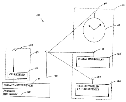
Fig. 1 shows a block diagram of a wireless synchronous time system according
to
the present invention including a master device which receives a GPS signal
and
broadcasts a time and programmed instruction to a system of slave devices;
Fig. 2 shows a block diagram of the master device of Fig. 1;
Fig. 3A shows a time package structure used in the transmission of the time
element of Fig. 1;
Fig. 313 shows a function package structure used in the transmission of the
programmed instruction element of Fig. 1;
Fig. 4 shows a block diagram of an analog clock slave device of Fig. 1;
Fig. 4A shows a clock movement box used in the setting of the slave clock of
Fig.
4;
Fig. 5 shows a block diagram of a slave device of Fig. 1, which includes a
switch
for controlling the functionality of the device; and
Fig. 6 shows a flow chart illustrating the functionality of a wireless
synchronous
time system in accordance with the present invention.
?0 Detailed DHon of the Dra ,wing
Referring to Fig. 1, a wireless synchronous time system 100 in accordance with
the
present invention includes a primary "mastor" device Z 10, which receives a
first time
signal through a receiving unit 115 and broadcasts a second time signal to a
plurality of
"slave" secondary event devices 130, The rracceiving unit 11 S includes a GPS
receiver 127
having an antenna 129 which receives a global positioning system ("GPS")
signal,
CA 02397278 2002-08-09
-5_
including a GPS time signal component. The recazving unit 115 sends the GPS
time signal
component to the primary master device 110 whore it is processed, as fiuther
discussed
b slow.
The primary master device 110 further includes a transmission unit 120, which
wirelessly transmits a signal to the secondary or "slave" devices 130. The
signal sent to
the slave devices 130 includes the processed GPS time signal component andJor
a
programmed instruction which is input to the primary master device 110 through
a
programmer input connection 125. The programmed instruction includes a
preprogrammed time element and a preprogrammed function element which, along
with
the GPS time signal component, is used by the primary master device 110 to
synchronize
the slave devices 134. The processed GPS time signal component and the
programmed
instruction are wirelessly transrnitted to the slave devices 130 at
approximately a
frequency between 72 and 7b MHz.
As shown in Fig. 1, examples of secondary or slave devices 130 include an
analog
time display 145, a digital time display 135, and a switching device 140,
which may be
associated with any one of a number of devices, such as a bell, a light, or a
lock, etc. Each
of the secondary devices 130 includes an antenna 150 to wirelessly receive the
processed
GPS time signal component and the programmed instruction from the primary
master
device 110. Each of the secondary devices 130 also includes a processor (see
Fig. 4,
? 0 element 410 and Fig. ~, element 525, not shoran in Fig. 1 ) to process
processed time signal
and the programmed instnaction received from the master device. As will be
fiuther
discussed below, when the preprogra~runed time elennent of the programmed
instntction
matches a second time generated by the slave device, an event will be
executed.
For the analog time display 145, shown in Fig. 1, the event will include
positioning
an hour, minute, and second hand to visually display the current time. For the
digital time
CA 02397278 2002-08-09
-6-
display 145, the ovcnt will include~digitally displaying the current time. For
the time
controlled switching device 140, the event may include any of a number of
events tvhich
may be controhed by the switch. For example, a system of bells may include
switches
which sound the bells at a particular time. Alternatively, a system of lights
may include
switches which turn the lights on or off' at a particular time, rt will be
readily apparent to
those of ordinary skill in the art that the slave devices may include any one
of a number of
electronic devices for which a particular functionality is desired to be
performed at a
particular time, such as televisions, radios, alectric door locks, etc.
Referring to Fig. 2, a detailed diagram of the primary master device 110 is
shown.
The primary master device 110 receives the GPS time signal component from the
receiving unit 115 (Fig. 1) at a GPS time signal input receiving unit or
connector 205. T'he
primary master device 110 further includes a processor 210, a memory 215, a
programmer
input connector 125, a display 225, a transmission unit 120, and a powered
input socket
235. These elements of the primary master device 110 serve to receive,
process, and
transmit the information used to synchronize the slave units 130, as will be
fully discussed
below. Additionally, a channel switch 245, time zone switch 250, and a
daylight savings
bypass switch Z55 arc included itt the primary master device 110. Lastly, the
primary
master device 110 includes a power interrupt module 258 coupled to the
processor 210 to
retain the internal time and the progrannmed instruction in the event of a
power loss_
:?0 Upon powering up the master device 110, the processor 210 checks the
setting of
the channel switch 245, the time zone switch 250, and the daylight savings
bypass switch
255. The processor 210 stores the switch inforrmation into the memory 215. A
GPS signal
is received through the GPS signal antenna 129 and a GPS time signal component
is
extracted from it. When the receiving unit or connector 205 receives the GPS
time signal
2S component, the processor 210 adjusts it according tv the switch information
of the channel
CA 02397278 2002-08-09
switch 245, the time zone switch 250, and the daylight savings bypass switch
255, and sets
an internal clock 260 to the processed GPS time signal component to produce a
first
internal time.
The channel switch 24S enables a user to select a particular transmission
frequency
determined best for transmission in the usage area, and to independently
operate additional
primary master devices in overlapping broadcast areas without causing
interference
between them. The GPS time signal uses a coordinated universal time ("UTC"),
and
requires a particular number of compensation hours to display the correct time
and date for
the desired time zone. The time zone switch 250 enables the user to select a
desired time
zone, and permits a worldwide usage. Lastly, the GPS time signal may not
include
daylight savings time information. A,s a result, users in areas that do not
require daylight
savings adjustment will be required to set the daylight savings bypass switch
2S5 to bypass
an automatic daylight savings adjustment program. Manual daylight savings time
adjustment can be accomplished by disconnecting the power source (not shown)
from the
1 ~ power input socket 235, adjusting the time zone switch 250 to the desired
time zone and
reconnecting the power source to the power input socket 235.
Once the processor Z 10 adjusts the GPS time signal component according to the
settings of the switches discussed above and sets the internal clock 260 to
produce the first
internal time, the internal clack 260 starts to increment the first internal
time until another
GPS time signal is received from the GPS receiver 12? (Fig. 1). Between
receiving GPS
tune signals, the internal clock 260 independently keeps the first internal
time which, in
addition to date information and reception status, is displayed on the display
225. In
addition to processing the time signal, the processor Z10 also checks for a
new
programmed instruction on a continuous basis, and stores any new programmed
instruction in the memory 215, As briefly me~ationed above, to enter a
programmed
CA 02397278 2002-08-09
.8.
instruction, a user keys in the programmed instruction into a computing device
(e.g., a
personal computer, a PDA, etc.) and txansfezs the programmed instruction to
the primary
master device 110 through the programmer input connector 125. The prograauned
instruction is stored in the memory 21 S and, along with the first internal
time kept in the
internal clock 260, is transmitted through the transmission unit 1 ~0 at the
transmission
frequency set in the channel switch 245.
The first internal time and the programmed instruction are transmitted by the
master device 110 using a data protocol as shown in Figs. 3A and 3B. Fig. 3A
shows a
time packet struetuxe 300 comprising of preprogrammed time element, and having
a 10-bit
preamble 304, a sync bit 308, a packet identity byte 312, an hour byte 316, a
minute byte
320, a second byte 324, a checksum byte 328 and a postamble bit 332. Fig. 3B
shows a
function packet structure 350 comprising a proprogrammed function element, and
laving a
10-bit preamble 354, a sync bit 358, a packet identity byte 362, an hour byte
366, a minute
byte 370, a function byte 374, a checksum byte 378, and a postamble bit 382.
Each
1 ~ secondary slave device i 30 will receive the signal broadcast by the
master device 110 and
including information according to the time packet structure of Fig. 3A and
the function
packet structure Fig. 3B. The secondary slave device will try to match the
packet identity
bytes 312 or 362 with an internal identity number programmed in its processor
(i.e., 410 of
Fig. 4 or 525 of Fig. 5) to selectively register the program instruction. It
should be readily
apparent to those of ordinary skill in the art that the time packet structure
300 and the
function packet structure 350 may have a different structure size so that more
or less
information may be transmitted using these packets. For e~camplc, the time
packet
structure may include, in addition to the existing timing bytes, a month byte,
a day byte, a
year byte, and a day of the week byte. Similarly, the function packet
structure 3 SO may
CA 02397278 2002-08-09
-9-
include additional hour, minute, and function bytes to terminate the execution
of an event
triggered by the hour, minute, and function bytes 366, 370, and 374, shown in
Fig. 3B.
Referring to Fig. 4, a diagram of the analog slave clock 145 of Fig. 1 is
shown.
The slave clock 145 includes a second receiving unit 402 having an antenna 1
S0 and a
S second receiver 406. The slave clock 145 also includes a second processor
410, a second
memory 41 S, a second internal clock 420 and an analog display 425, including
a set of
hands 430 including a second hand 432, a rninutc hand 434, and an hour hand
436. As
with the master device 110, the secondary slave clock 145 also includes a
power intetntpt
module 438 coupled to the processor 410 to retain an internal tune and a
programmed
instruction in the event of a power loss to the slave clock 145.
Fig. 4A illustrates a clock movomcnt box 450 having a manual rime set wheel
465,
and a push button 470 for setting the position of the hands 430 of the analog
display 425.
The clock movement box 450 is of the type typically found on the back of
conventional
analog display wall clocks, and is used to set such clocks. In setting the
analog slave clock
145, the manual time set wheel 465 of the clock movement box 450 is initiahy
turned anti f
the set of hands 430 shows a time within 29 minutes of the GPS time (i.e., the
actual time).
'When power is applied to the slave analog clock 145, the second hand 432
starts to step.
The push button 470 of the clock movement box 450 is depressed when the second
hand
reaches the 12 o'clock position. This signals to the second processor 410 that
the second
hand 432 is at the 12 o'clock position, enabling the second processor 410 to
"lrnow" the
location of the second hand 432. The push button 470 is again depressed when
the second
hand 432 crosses over the minute hand 434, wherever it may be. This enables
the second
processor 410 to "know" the location of the minute hand 434 on the clock dial.
(See U.S.
Patent Application No. 09!645,974 to O'Neill, the disclosure of which is
incorporated by
2~ reference herein).
CA 02397278 2002-08-09
-10-
To synchronize itself to the master device I 10, the second receiver 406 of
the slave
device 145 autonnatically and continuously searches a transmission frequency
or a channel
that contains the first internal time and the programmed instruction. When the
receiving
unit 402 wirelcssly receives and identifies the first interzial time, the
processor 410 stores
the received first internal time at the second internal clock 420. The second
internal clock
420 irximediately starts to increment to produce a second internal time. Tue
second
internal time is kept by the second internal clock 420 until another first
internal time signal
is received by the slave clock 145. If the processor 410 determines that the
set of hands
430 displays a lag time (i.e., since a first internal time signal was last
received by the slave
clock 145, the second internal clock 420 had fallen behind), the processor 410
speeds up
the second hand 432 frazn one step per second to eight steps per second until
both the
second hand 432 and the minute hand 434 agree with the newly established
second
internal time. If the processor 410 determines that the set of hands 430 shows
a lead time
(i.e., since the first internal time signal was last received by the slave
clock 145, the second
1 ~ internal clock 420 had moved faster than the time signal relayed by the
master device), the
processor 410 slows down the second hand 432 from one step per second to one
step per
five seconds until both the second hand 432 and the minute hand 434 agree with
the newly
established second interns! time.
In additional to slave clocks which simply display the synchronized time
signal, a
?4 slave device 130 may include the switching slave device 144 depicted in
Fig. 5. Instead of
simply displaying the time signal, the switching slave device 140 utilizes the
time signal to
execute an event at a particular time. Irr this way, a system of slave
switching devices can
be synchronized. The slave switching device 140 includes a second receiving
unit 51 U
having an antenna ISO and a second receiver 524, a second processor 525, a
second
2S internal clock 530, a second memory 535, an operating switch 540, and a
device power
CA 02397278 2002-08-09
-11-
source 550. The secondary stave swvitching device 140 fzuther includes a power
interrupt
module 552 coupled to the processor 410 to retain the intarnal time and the
programmed
instruction on a continuous basis, similar to the power interrupt module of
the master
device 110 and the slave clock 145. '),he secondary slave switching device 140
includes
any one of a number of devices 555, which is to be synchronously controlled.
Depending
upon the device 5S5 to be controlled, a first end 560 of the device is coupled
tv a normally
open end ("NO"j 565 or a normally closed end {"NC"j 570 of the operating
switch 540.
The first power lead 575 of the device power source 55:0 is then coupled to a
second end
580 of the device 555, while a second power lead 585 of the device power
source 550 is
L O coupled to the normally open end 565 or the normally closod end 570 of the
operating
switch 540 to complete the circuit.
Like the receiver 406 of the slave clock 145, the second receiver 520 of the
slave
switching device 140 automatically searches a transmission frequency or a
channel that
contains a first internal time and a prog~Cammed instruction from the master
device 110.
When the receiving unit 510 wirelessly receives and identifies the first
internal time, the
second processor 525 stores the received first internal time in a second
internal clock 530.
The second internal clock 530 irnmediatsly starts to increment to produce a
second internal
tune until another first internal time signal is received from the roaster
device 110.
Additionally, the programxrted instruction is stored in the memory 535. When
there is a
match between the second internal time and the preprogrammed time element of
the
programmed instnretion, the preprogrammed function element will be executed.
For
example, if the preprogrammed time element contains a time of day, and the
preprogramrix~d functional element contains an instruction to switch on a
light, the light
will be switched on when the second internal clock 530 reaches that time
specified in the
preprogtatnrned time elcmmt of the programmed instruction.
CA 02397278 2002-08-09
-12-
Referring to Fig. 6, a flow chart 600 illustrates a wireless synchronous time
system
according to the present invention. The flow chart 600 illustrates the steps
performed by a
wireless synchronous time system according to the present invention for any
number of
systems of slave devices. The process starts in a receiving step 610 where a
master device
S receives a GPS time signal. As indicated in the flow chart at step 610, the
master device
will continuously look for and receive new CAPS time signals. Next, at step 61
S a first
internal clock is set to the received GPS time. Next, the first internal clock
will start to
increment a first internal time in step 620. In a parallel pat$, at step 625,
the master device
receives programmed instructions input by a user of the system. Again, the
flow chart
indicates that the master device is able to continuously receive programmed
instntction so
that a user may add additional programmed instructions to the system at any
time. As
discussed above, the programmed instructions will include a preprogrammed time
element
and a preprogrammed function elemecxt. The programmed instruction is then
stored in a
first memory at step 627. Next, when preset periodic times are reached at step
629, the
1 ~ programmed instruction is retrieved at step 630 and transmitted at step
632 to the slave
device along with the first internal time at step 635. In other words, when
the first internal
clock reaches particular preset times (e.g., every $ve minutes) the programmed
instruction
and the first internal time are wirelessly transmitted to the slave devices.
The programmed instruction and/or the first internal time arc received at the
slave
'?0 device in step 640. if the slave device is to merely synchronously display
a time, such as a
clock, but does not perform any funetior~ality, there is no need to receive
the programmed
instruction. In slave devices such as bells, lights, locks, etc., in addition
to the first internal
time, at step 642, the processor will select those programmed instructions
whoa the packet
identity byte matches with the.slave devices identity. The selected programmed
25 instruction is then stored or registered in the memozy at the secondary
slave device in step
CA 02397278 2002-08-09
-13-
645. A second internal clock is then set to the first internal time at step
650 to produce a
second internal time. In step 655, like the first internal clock, the second
internal clock
will start to increment the second internal time. The second internal time is
displayed at
step 655. Meanwhile, a function is identified >som the preprogrannned function
element at
step 670. When, the second internal time has incremented to match the
preprogratnzned
time element at step 675, the function will be executed in step 6g0.
Otherwise, the
secondary slave device will continue to compare the second internal time with
the
preprogrammed time element until a match is identified.
It will be readily trrrderstood by those of ordinary skill in the art, that
both the first
1 U internal clock and the second internal clock increment, and thus keep a
relatively current
time, independently. Therefore, if, for some reason, the master device does
not receive an
updated GPS time signal, it will still be able to transmit the first internal
time. Similarly,
if, for some reason, the slave device does not receive a signal from the
master device, the
second internal clock will still maintain a relatively current time. In this
way, the slave
l > device will still display a relatively aurre~nt time and/or execute a
particular function at a
relatively accurate time even, if the wireless communication with the master
device is
interrupted. Additionally, the roaster device will broadcast a relatively
current time and a
relatively current programmed instruction even if the wireless communicahion
with a
satellite broadcasting the GPS signal is interrupted. Furthermore, the power
interrupt
20 modules of the master and slave devicos help keep the system relarively
synchronized in
the event of power interruption to the slave and/or master devices.
It is to be understood that the invention is not limited in its application to
the
details of construction and the arrangement of components set forth in the
above
description or illustrated in the drawings. The invention is capable of other
embodiments
25 and of being practiced or being catxied out in various ways. Also, it is to
be understood
CA 02397278 2002-08-09
-14-
that the phraseology and terminology used herein is for the purpose'of
description and
should not be regarded as limited. The use of "including" and "comprising" and
variations
thereof herein is meant to encompass the items listed thereafter in accordance
thereof as
well as additional items. Although the invention has been described in detail
with
reference to certain preferred embodiments, variations and modifications exist
within the
scope and spirit of the invention as described and defined in the following
claims.