Note: Descriptions are shown in the official language in which they were submitted.
CA 02397760 2002-07-17
WO 01/54176 PCT/USO1/01758
WAFER BONDING TECHNIQUES TO MINIMIZE BUILT-IN STRESS OF
SILICON MICROSTRUCTURES AND MICRO-MIRRORS
CROSS REFERENCE TO RELATED APPLICATIONS
This application claims priority from the following
U.S. Provisional Patent Application, the disclosure of which is
incorporated by reference in its entirety for all purposes:
U.S. Provisional Patent Application Serial No.
60/176,325, entitled "New Wafer Bonding Techniques to Minimize
Built-in Stress of Silicon Microstructures and Micro Mirrors,"
filed January 18, 2000.
BACKGROUND OF THE INVENTION
The invention relates to the fabrication of Silicon-
On-Insulator (SOI) structures.
There is great interest in making small opto-
mechanical structures out of SOI material using micromachining
techniques. One type of SOI wafer is a bonded SOI wafer. Often
a bonded SOI wafer is manufactured as two wafers, a device wafer
and a handle wafer. The handle wafer is thermally oxidized to
form on its surface an oxide layer. Both wafers are chemically
treated to become hydrophilic, are aligned and their polished
surfaces allowed to come into contact. The wafers adhere to
each other and, after a high temperature annealing process, are
strongly bonded together. The bonded water is ground ana
polished to form a finished wafer consisting of a handle wafer,
an intermediate buried oxide and a device silicon wafer. The
device wafer can typically range from less than one micron to
several tens of microns in thickness.
CA 02397760 2002-07-17
WO 01/54176 PCT/USO1/01758
Prior scanners use a single crystal SOI fabricated
mirror. Generally, to produce a moveable mirror in SOI
material, the silicon of the handle wafer is etched away from
beneath the device layer and the buried oxide layer serves as a
convenient hard etch stop layer during this process. The
remaining thin device layer of silicon is etched to form a one-
or two-dimensional moveable mirror, as described in U.S. Patent
5,629,790, to Neukermans et al.
Although a silicon mirror should have nearly zero
stress and therefore present an optically flat surface,
conventional SOI wafer manufacturing processes can affect the
flatness of the silicon device layer. Detailed interferometric
measurements of the flatness of silicon mirrors approximately
1.5 by 2.1 mm made of bonded SOI material 10 um thick show a
non-flatness of up to 0.3 waves (lambda=633um) when fabricated
using the standard technology. For very large flat mirrors that
are extremely thin as required in many applications, this
flatness is not adequate.
SUMMARY OF THE INVENTION
In one aspect of the invention,a method of fabricating
a Silicon-On-Insulator (SOI) bonded wafer structure includes
oxidizing a device silicon wafer and bonding the oxidized device
silicon wafer to a handle silicon wafer.
Embodiments of the invention may include one or more
of the following features.
Fabricating the SOI bonded wafer structure can further
include lapping the device silicon wafer down to a desired
thickness and etching the device silicon wafer to define a
mirror.
2
CA 02397760 2002-07-17
WO 01/54176 PCT/USO1/01758
Fabricating the SOI bonded wafer structure can further
include oxidizing the handle silicon wafer prior to bonding the
oxidized device silicon wafer to the handle silicon wafer.
The oxidizing of the handler silicon wafer and the
oxidizing of the device silicon wafer can each result in oxide
films approximately equal to one-half of a desired thickness.
The device silicon wafer, the handle silicon wafer, or
both of the silicon wafers can be made of polysilicon.
Among the advantages of the present invention are the
following. If the buried oxide layer is grown on the device
wafer instead of the handle wafer, the flatness of a silicon
mirror fabricated with an SOI manufacturing process so modified
may be substantially improved. Similar results may be obtained
if an oxide film half the desired thickness is grown on both the
handle and device wafers, or the oxide film is split between the
two wafers in some other manner.
Other features and advantages of the invention will be
apparent from the following detailed description and from the
claims.
BRIEF DESCRIPTION OF THE DRAWINGS
FIG. 1 is a side view of a prior art silicon bonded
wafer structure.
FIG. 2 is a side view of micro-mirror structure
fabricated from a silicon bonded wafer structure.
FIG. 3 is a side view of a silicon bonded wafer
structure fabricated using a thermally oxidized device wafer.
FIG. 4 is a side view of a silicon bonded wafer
structure fabricated using thermally oxidized handle and device
wafers.
3
CA 02397760 2002-07-17
WO 01/54176 PCT/USO1/01758
FIG. 5 is a side view of a bonded wafer structure
fabricated using polysilicon instead of single crystal silicon
as the device wafer.
FIG. 6 is a schematic depiction of polysilicon
resistive sensors arranged in a Wheatstone bridge arrangement
for measuring torque.
DETAILED DESCRIPTION
Referring to FIG. l, a prior art silicon bonded wafer
structure 10 including a set of bonded wafers, more
particularly, a handle wafer 12 and a device wafer 14, separated
by an oxide layer 16, is shown. Using conventional fabrication
techniques, the wafers are bonded as follows. The handle wafer
12 is thermally oxidized to form the oxide layer 16, which
typically has a thickness of a few thousand Angstrom. The
device wafer 14 is bonded to the oxidized handle wafer 12. Once
bonded, the device wafer 14 is lapped down or otherwise thinned
to a required thickness.
Referring to FIG. 2, a micro-mirror structure 20
produced from the silicon bonded wafer structure 10 (of FIG. 1)
is shown. To transform the silicon bonded wafer structure 10 to
the micro-mirror structure 20, etching is performed and a
moveable mirror 32 is defined in the device wafer 14. This
process is described in U.S. Patent Application Serial Nos.
5,629,790 and 6,044,705, both to Neukermans et al., both
incorporated herein by reference. It is found that for very
large thin mirrors (e. g., several mm in size and 2-10 micron
thick) produced by this process, there are some residual
stresses that make such mirrors marginal for use in very
-4-
CA 02397760 2002-07-17
WO 01/54176 PCT/USO1/01758
demanding optical applications.
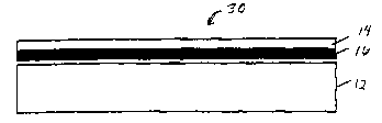
Referring to FIG. 3, an enhanced silicon bonded wafer
structure 30 includes the handle wafer 12, the device wafer 14
and the oxide layer 16 disposed therebetween. In order to
fabricate the enhanced silicon bonded wafer structure 30, the
device wafer 14 is thermally oxidized to form the oxide layer
16. The oxidized device wafer 14 and handle wafer 12 are
bonded, and the device wafer 14 is thinned. A micro-mirror
structure is provided from the silicon bonded wafer structure 30
using techniques as shown and described in FIG. 2. The mirrors
manufactured on the silicon bonded wafer structure 30 are much
flatter than those manufactured using conventionally provided a
set of bonded wafers.
Other embodiments are contemplated. For example, and
with reference to FIG. 4, both the handle wafer 12 and the
device wafer 14 can be oxidized to form the oxide layer 16 prior
to bonding. The wafers 12, 14 may be oxidized with the same or
different thickness. Preferably, the thickness of the oxide
grown on the handle wafer 12 is equal to or less than the
thickness of the oxide grown on the device wafer 14.
Specifically, using a buried oxide layer of 4000A and
a device wafer or device silicon layer of 10 microns, a mirror
1.5 by 2.1 mm shows an average non-flatness (lambda=633nm) of:
0.22 waves when the handle wafer is oxidized 4000A; 0.11 waves
when the device wafer is oxidized 4000A; and 0.12 waves when the
handle and device wafers are both oxidized 2000A.
Removal of an interfacial silicon layer on the device
wafer 16 by a very short chemical etch after removing the buried
oxide layer further relieves built-in stresses.
-5-
CA 02397760 2002-07-17
WO 01/54176 PCT/USO1/01758
Although not shown, a single crystal silicon device
layer also allows for the incorporation of high sensitivity
shear sensors, which allow the positioning of mirrors in micro-
mirror structures like the one shown in FIG. 2 with great
accuracy.
In yet another embodiment, an SOI structure that
includes polysilicon is used to produce a more ductile material.
Referring to FIG. 5, a silicon bonded wafer structure
50 includes the handle wafer 12 and the oxide wafer 16, but the
single crystal device wafer 14 (of FIGS. 1-4) is replaced by a
polysilicon device wafer 52, of the same size. The polysilicon
wafer 52 is lapped down to the desired thickness and, after
etching, gives rise to the structure 50. The top layer 52 is
polysilicon, and, as before, the intermediate layer 16 is oxide
and the bottom layer 12 is a single crystal silicon layer. The
polysilicon wafer yields a thick (5-100 micron), stress free
layer of polysilicon that is suitable as a mirror plate. The
resultant layer of polysilicon is then treated as the single
crystal layer for purposes of mirror construction. The
polysilicon layer can be used to define polysilicon hinge
sensors as well, and in the same manner as single crystal
silicon.
The handle wafer 12 can also be made of polysilicon.
Thus, one or both of the wafers 12, 14 can be made of
polysilicon and an oxide formed on the device wafer 14 (whether
it be made of polysilicon or single crystal silicon) as
described above.
Referring to FIG. 6, a partial view of a hinge 60
shows four polysilicon resistive sensors 62 placed in a
-6-
CA 02397760 2002-07-17
WO 01/54176 PCT/USO1/01758
Wheatstone bridge type arrangement 64 so that the output
corresponds to a shear measurement, that is, the diagonal axis
of the Wheatstone bridge 64 is along the direction of hinge 62.
Applying voltage to a-a produces an output b-b if shear is
present. This arrangement is similar to that of measuring
torque with classical strain gauges. It may be noted that the
polysilicon hinge sensors are not as sensitive as those made
from the single crystal silicon.
Other embodiments are within the scope of the
to following claims.
What is claimed is: