Sélection de la langue

Search

Sommaire du brevet 2397760 

Énoncé de désistement de responsabilité concernant l'information provenant de tiers

Une partie des informations de ce site Web a été fournie par des sources externes. Le gouvernement du Canada n'assume aucune responsabilité concernant la précision, l'actualité ou la fiabilité des informations fournies par les sources externes. Les utilisateurs qui désirent employer cette information devraient consulter directement la source des informations. Le contenu fourni par les sources externes n'est pas assujetti aux exigences sur les langues officielles, la protection des renseignements personnels et l'accessibilité.

Disponibilité de l'Abrégé et des Revendications

L'apparition de différences dans le texte et l'image des Revendications et de l'Abrégé dépend du moment auquel le document est publié. Les textes des Revendications et de l'Abrégé sont affichés :

  • lorsque la demande peut être examinée par le public;
  • lorsque le brevet est émis (délivrance).
(12) Demande de brevet: (11) CA 2397760
(54) Titre français: LIAGE DESTINE A MINIMISER LA CONTRAINTE INTEGREE DES MICROSTRUCTURES ET DES MICROMIROIRS EN SILICIUM
(54) Titre anglais: WAFER BONDING TECHNIQUES TO MINIMIZE BUILT-IN STRESS OF SILICON MICROSTRUCTURES AND MICRO-MIRRORS
Statut: Réputée abandonnée et au-delà du délai pour le rétablissement - en attente de la réponse à l’avis de communication rejetée
Données bibliographiques
(51) Classification internationale des brevets (CIB):
  • H01L 21/20 (2006.01)
  • H01L 21/762 (2006.01)
(72) Inventeurs :
  • SLATER, TIMOTHY G. (Etats-Unis d'Amérique)
(73) Titulaires :
  • XROS, INC.
(71) Demandeurs :
  • XROS, INC. (Etats-Unis d'Amérique)
(74) Agent: SMART & BIGGAR LP
(74) Co-agent:
(45) Délivré:
(86) Date de dépôt PCT: 2001-01-18
(87) Mise à la disponibilité du public: 2001-07-26
Licence disponible: S.O.
Cédé au domaine public: S.O.
(25) Langue des documents déposés: Anglais

Traité de coopération en matière de brevets (PCT): Oui
(86) Numéro de la demande PCT: PCT/US2001/001758
(87) Numéro de publication internationale PCT: US2001001758
(85) Entrée nationale: 2002-07-17

(30) Données de priorité de la demande:
Numéro de la demande Pays / territoire Date
09/715,916 (Etats-Unis d'Amérique) 2000-11-16
60/176,325 (Etats-Unis d'Amérique) 2000-01-18

Abrégés

Abrégé français

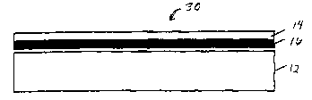
L'invention concerne un procédé de fabrication d'une tranche liée pour une structure micromiroir destinée à réduire par l'oxyde une tranche de dispositif au lieu d'une tranche de manipulation ou à séparer le traitement d'oxydation thermique entre la tranche de dispositif et la tranche de manipulation avant la gravure. La planéité des miroirs dans les structures micromiroirs fabriquées selon ce procédé est sensiblement améliorée.


Abrégé anglais


A bonded wafer fabrication mechanism for a micro-mirror structure provides for
oxidizing a device wafer instead of a handle wafer or splitting thermal
oxidation processing between the device wafer and the handle wafer prior to
etching. The flatness of mirrors in micro-mirror structures fabricated
according to such a mechanism is substantially improved.

Revendications

Note : Les revendications sont présentées dans la langue officielle dans laquelle elles ont été soumises.


1. A method of fabricating a Silicon-On-Insulator (SOI)
bonded wafer structure comprising:
oxidizing a surface portion of a device silicon wafer;
and
bonding the oxidized surface portion of the device
silicon wafer to a handle silicon wafer.
2. The method of claim 1, further comprising:
lapping the device silicon wafer down to a desired
thickness; and
etching the device silicon wafer to define a mirror.
3. The method of claim 2, further comprising:
oxidizing the handle silicon wafer prior to bonding
the oxidized device silicon wafer to the handle silicon wafer.
4. The method of claim 3, wherein the oxidizing of the
handler silicon wafer and the oxidizing of the device silicon
wafer each result in oxide films approximately equal to one-half
of a desired thickness.
5. The method of claim 1, wherein the device silicon
wafer is made of single crystal silicon.
6. The method of claim 1, wherein the handle silicon
wafer is made of single crystal silicon.
-8-

Description

Note : Les descriptions sont présentées dans la langue officielle dans laquelle elles ont été soumises.


CA 02397760 2002-07-17
WO 01/54176 PCT/USO1/01758
WAFER BONDING TECHNIQUES TO MINIMIZE BUILT-IN STRESS OF
SILICON MICROSTRUCTURES AND MICRO-MIRRORS
CROSS REFERENCE TO RELATED APPLICATIONS
This application claims priority from the following
U.S. Provisional Patent Application, the disclosure of which is
incorporated by reference in its entirety for all purposes:
U.S. Provisional Patent Application Serial No.
60/176,325, entitled "New Wafer Bonding Techniques to Minimize
Built-in Stress of Silicon Microstructures and Micro Mirrors,"
filed January 18, 2000.
BACKGROUND OF THE INVENTION
The invention relates to the fabrication of Silicon-
On-Insulator (SOI) structures.
There is great interest in making small opto-
mechanical structures out of SOI material using micromachining
techniques. One type of SOI wafer is a bonded SOI wafer. Often
a bonded SOI wafer is manufactured as two wafers, a device wafer
and a handle wafer. The handle wafer is thermally oxidized to
form on its surface an oxide layer. Both wafers are chemically
treated to become hydrophilic, are aligned and their polished
surfaces allowed to come into contact. The wafers adhere to
each other and, after a high temperature annealing process, are
strongly bonded together. The bonded water is ground ana
polished to form a finished wafer consisting of a handle wafer,
an intermediate buried oxide and a device silicon wafer. The
device wafer can typically range from less than one micron to
several tens of microns in thickness.

CA 02397760 2002-07-17
WO 01/54176 PCT/USO1/01758
Prior scanners use a single crystal SOI fabricated
mirror. Generally, to produce a moveable mirror in SOI
material, the silicon of the handle wafer is etched away from
beneath the device layer and the buried oxide layer serves as a
convenient hard etch stop layer during this process. The
remaining thin device layer of silicon is etched to form a one-
or two-dimensional moveable mirror, as described in U.S. Patent
5,629,790, to Neukermans et al.
Although a silicon mirror should have nearly zero
stress and therefore present an optically flat surface,
conventional SOI wafer manufacturing processes can affect the
flatness of the silicon device layer. Detailed interferometric
measurements of the flatness of silicon mirrors approximately
1.5 by 2.1 mm made of bonded SOI material 10 um thick show a
non-flatness of up to 0.3 waves (lambda=633um) when fabricated
using the standard technology. For very large flat mirrors that
are extremely thin as required in many applications, this
flatness is not adequate.
SUMMARY OF THE INVENTION
In one aspect of the invention,a method of fabricating
a Silicon-On-Insulator (SOI) bonded wafer structure includes
oxidizing a device silicon wafer and bonding the oxidized device
silicon wafer to a handle silicon wafer.
Embodiments of the invention may include one or more
of the following features.
Fabricating the SOI bonded wafer structure can further
include lapping the device silicon wafer down to a desired
thickness and etching the device silicon wafer to define a
mirror.
2

CA 02397760 2002-07-17
WO 01/54176 PCT/USO1/01758
Fabricating the SOI bonded wafer structure can further
include oxidizing the handle silicon wafer prior to bonding the
oxidized device silicon wafer to the handle silicon wafer.
The oxidizing of the handler silicon wafer and the
oxidizing of the device silicon wafer can each result in oxide
films approximately equal to one-half of a desired thickness.
The device silicon wafer, the handle silicon wafer, or
both of the silicon wafers can be made of polysilicon.
Among the advantages of the present invention are the
following. If the buried oxide layer is grown on the device
wafer instead of the handle wafer, the flatness of a silicon
mirror fabricated with an SOI manufacturing process so modified
may be substantially improved. Similar results may be obtained
if an oxide film half the desired thickness is grown on both the
handle and device wafers, or the oxide film is split between the
two wafers in some other manner.
Other features and advantages of the invention will be
apparent from the following detailed description and from the
claims.
BRIEF DESCRIPTION OF THE DRAWINGS
FIG. 1 is a side view of a prior art silicon bonded
wafer structure.
FIG. 2 is a side view of micro-mirror structure
fabricated from a silicon bonded wafer structure.
FIG. 3 is a side view of a silicon bonded wafer
structure fabricated using a thermally oxidized device wafer.
FIG. 4 is a side view of a silicon bonded wafer
structure fabricated using thermally oxidized handle and device
wafers.
3

CA 02397760 2002-07-17
WO 01/54176 PCT/USO1/01758
FIG. 5 is a side view of a bonded wafer structure
fabricated using polysilicon instead of single crystal silicon
as the device wafer.
FIG. 6 is a schematic depiction of polysilicon
resistive sensors arranged in a Wheatstone bridge arrangement
for measuring torque.
DETAILED DESCRIPTION
Referring to FIG. l, a prior art silicon bonded wafer
structure 10 including a set of bonded wafers, more
particularly, a handle wafer 12 and a device wafer 14, separated
by an oxide layer 16, is shown. Using conventional fabrication
techniques, the wafers are bonded as follows. The handle wafer
12 is thermally oxidized to form the oxide layer 16, which
typically has a thickness of a few thousand Angstrom. The
device wafer 14 is bonded to the oxidized handle wafer 12. Once
bonded, the device wafer 14 is lapped down or otherwise thinned
to a required thickness.
Referring to FIG. 2, a micro-mirror structure 20
produced from the silicon bonded wafer structure 10 (of FIG. 1)
is shown. To transform the silicon bonded wafer structure 10 to
the micro-mirror structure 20, etching is performed and a
moveable mirror 32 is defined in the device wafer 14. This
process is described in U.S. Patent Application Serial Nos.
5,629,790 and 6,044,705, both to Neukermans et al., both
incorporated herein by reference. It is found that for very
large thin mirrors (e. g., several mm in size and 2-10 micron
thick) produced by this process, there are some residual
stresses that make such mirrors marginal for use in very
-4-

CA 02397760 2002-07-17
WO 01/54176 PCT/USO1/01758
demanding optical applications.
Referring to FIG. 3, an enhanced silicon bonded wafer
structure 30 includes the handle wafer 12, the device wafer 14
and the oxide layer 16 disposed therebetween. In order to
fabricate the enhanced silicon bonded wafer structure 30, the
device wafer 14 is thermally oxidized to form the oxide layer
16. The oxidized device wafer 14 and handle wafer 12 are
bonded, and the device wafer 14 is thinned. A micro-mirror
structure is provided from the silicon bonded wafer structure 30
using techniques as shown and described in FIG. 2. The mirrors
manufactured on the silicon bonded wafer structure 30 are much
flatter than those manufactured using conventionally provided a
set of bonded wafers.
Other embodiments are contemplated. For example, and
with reference to FIG. 4, both the handle wafer 12 and the
device wafer 14 can be oxidized to form the oxide layer 16 prior
to bonding. The wafers 12, 14 may be oxidized with the same or
different thickness. Preferably, the thickness of the oxide
grown on the handle wafer 12 is equal to or less than the
thickness of the oxide grown on the device wafer 14.
Specifically, using a buried oxide layer of 4000A and
a device wafer or device silicon layer of 10 microns, a mirror
1.5 by 2.1 mm shows an average non-flatness (lambda=633nm) of:
0.22 waves when the handle wafer is oxidized 4000A; 0.11 waves
when the device wafer is oxidized 4000A; and 0.12 waves when the
handle and device wafers are both oxidized 2000A.
Removal of an interfacial silicon layer on the device
wafer 16 by a very short chemical etch after removing the buried
oxide layer further relieves built-in stresses.
-5-

CA 02397760 2002-07-17
WO 01/54176 PCT/USO1/01758
Although not shown, a single crystal silicon device
layer also allows for the incorporation of high sensitivity
shear sensors, which allow the positioning of mirrors in micro-
mirror structures like the one shown in FIG. 2 with great
accuracy.
In yet another embodiment, an SOI structure that
includes polysilicon is used to produce a more ductile material.
Referring to FIG. 5, a silicon bonded wafer structure
50 includes the handle wafer 12 and the oxide wafer 16, but the
single crystal device wafer 14 (of FIGS. 1-4) is replaced by a
polysilicon device wafer 52, of the same size. The polysilicon
wafer 52 is lapped down to the desired thickness and, after
etching, gives rise to the structure 50. The top layer 52 is
polysilicon, and, as before, the intermediate layer 16 is oxide
and the bottom layer 12 is a single crystal silicon layer. The
polysilicon wafer yields a thick (5-100 micron), stress free
layer of polysilicon that is suitable as a mirror plate. The
resultant layer of polysilicon is then treated as the single
crystal layer for purposes of mirror construction. The
polysilicon layer can be used to define polysilicon hinge
sensors as well, and in the same manner as single crystal
silicon.
The handle wafer 12 can also be made of polysilicon.
Thus, one or both of the wafers 12, 14 can be made of
polysilicon and an oxide formed on the device wafer 14 (whether
it be made of polysilicon or single crystal silicon) as
described above.
Referring to FIG. 6, a partial view of a hinge 60
shows four polysilicon resistive sensors 62 placed in a
-6-

CA 02397760 2002-07-17
WO 01/54176 PCT/USO1/01758
Wheatstone bridge type arrangement 64 so that the output
corresponds to a shear measurement, that is, the diagonal axis
of the Wheatstone bridge 64 is along the direction of hinge 62.
Applying voltage to a-a produces an output b-b if shear is
present. This arrangement is similar to that of measuring
torque with classical strain gauges. It may be noted that the
polysilicon hinge sensors are not as sensitive as those made
from the single crystal silicon.
Other embodiments are within the scope of the
to following claims.
What is claimed is:

Dessin représentatif
Une figure unique qui représente un dessin illustrant l'invention.
États administratifs

2024-08-01 : Dans le cadre de la transition vers les Brevets de nouvelle génération (BNG), la base de données sur les brevets canadiens (BDBC) contient désormais un Historique d'événement plus détaillé, qui reproduit le Journal des événements de notre nouvelle solution interne.

Veuillez noter que les événements débutant par « Inactive : » se réfèrent à des événements qui ne sont plus utilisés dans notre nouvelle solution interne.

Pour une meilleure compréhension de l'état de la demande ou brevet qui figure sur cette page, la rubrique Mise en garde , et les descriptions de Brevet , Historique d'événement , Taxes périodiques et Historique des paiements devraient être consultées.

Historique d'événement

Description Date
Le délai pour l'annulation est expiré 2006-01-18
Demande non rétablie avant l'échéance 2006-01-18
Réputée abandonnée - omission de répondre à un avis sur les taxes pour le maintien en état 2005-01-18
Lettre envoyée 2004-05-10
Inactive : Supprimer l'abandon 2004-05-10
Inactive : Demandeur supprimé 2004-05-07
Inactive : Abandon. - Aucune rép. à lettre officielle 2004-03-15
Inactive : Correspondance - Transfert 2004-03-02
Inactive : Renseignement demandé pour transfert 2003-12-15
Inactive : Supprimer l'abandon 2003-11-28
Inactive : Transfert individuel 2003-10-21
Inactive : Abandon. - Aucune rép. à lettre officielle 2003-10-21
Inactive : Page couverture publiée 2003-01-15
Inactive : Lettre de courtoisie - Preuve 2002-12-10
Inactive : Notice - Entrée phase nat. - Pas de RE 2002-12-03
Inactive : Demandeur supprimé 2002-12-03
Demande reçue - PCT 2002-09-21
Exigences pour l'entrée dans la phase nationale - jugée conforme 2002-07-17
Demande publiée (accessible au public) 2001-07-26

Historique d'abandonnement

Date d'abandonnement Raison Date de rétablissement
2005-01-18

Taxes périodiques

Le dernier paiement a été reçu le 2003-12-12

Avis : Si le paiement en totalité n'a pas été reçu au plus tard à la date indiquée, une taxe supplémentaire peut être imposée, soit une des taxes suivantes :

  • taxe de rétablissement ;
  • taxe pour paiement en souffrance ; ou
  • taxe additionnelle pour le renversement d'une péremption réputée.

Les taxes sur les brevets sont ajustées au 1er janvier de chaque année. Les montants ci-dessus sont les montants actuels s'ils sont reçus au plus tard le 31 décembre de l'année en cours.
Veuillez vous référer à la page web des taxes sur les brevets de l'OPIC pour voir tous les montants actuels des taxes.

Historique des taxes

Type de taxes Anniversaire Échéance Date payée
Taxe nationale de base - générale 2002-07-17
TM (demande, 2e anniv.) - générale 02 2003-01-20 2003-01-03
Enregistrement d'un document 2003-10-21
TM (demande, 3e anniv.) - générale 03 2004-01-19 2003-12-12
Titulaires au dossier

Les titulaires actuels et antérieures au dossier sont affichés en ordre alphabétique.

Titulaires actuels au dossier
XROS, INC.
Titulaires antérieures au dossier
TIMOTHY G. SLATER
Les propriétaires antérieurs qui ne figurent pas dans la liste des « Propriétaires au dossier » apparaîtront dans d'autres documents au dossier.
Documents

Pour visionner les fichiers sélectionnés, entrer le code reCAPTCHA :


Pour visualiser une image, cliquer sur un lien dans la colonne description du document. Pour télécharger l'image (les images), cliquer l'une ou plusieurs cases à cocher dans la première colonne et ensuite cliquer sur le bouton "Télécharger sélection en format PDF (archive Zip)" ou le bouton "Télécharger sélection (en un fichier PDF fusionné)".

Liste des documents de brevet publiés et non publiés sur la BDBC .

Si vous avez des difficultés à accéder au contenu, veuillez communiquer avec le Centre de services à la clientèle au 1-866-997-1936, ou envoyer un courriel au Centre de service à la clientèle de l'OPIC.


Description du
Document 
Date
(aaaa-mm-jj) 
Nombre de pages   Taille de l'image (Ko) 
Dessin représentatif 2002-07-16 1 2
Abrégé 2002-07-16 1 56
Dessins 2002-07-16 2 21
Revendications 2002-07-16 1 25
Description 2002-07-16 7 253
Rappel de taxe de maintien due 2002-12-02 1 106
Avis d'entree dans la phase nationale 2002-12-02 1 189
Demande de preuve ou de transfert manquant 2003-07-20 1 101
Courtoisie - Certificat d'enregistrement (document(s) connexe(s)) 2004-05-09 1 105
Courtoisie - Lettre d'abandon (taxe de maintien en état) 2005-03-14 1 174
Rappel - requête d'examen 2005-09-19 1 116
PCT 2002-07-16 4 138
Correspondance 2002-12-02 1 25
PCT 2002-07-17 4 146
PCT 2002-07-17 4 167
Correspondance 2003-12-14 1 21