Note: Descriptions are shown in the official language in which they were submitted.
CA 02398359 2002-07-24
WO 01/67497 PCT/GBO1/00904
1
QUANTUM WELL INTERMIXING
Background to the Invention
The monolithic integration of several optoelectronics
devices in optoelectronics integrated circuits (OETCs) and
photonic integrated circuits (PICs) is of considerable
interest for the development of telecommunications systems.
In OEICs, optical devices such as lasers and
electronic devices such as transistors are integrated on a
single chip for high speed operation since parasitic
reactance in the electrical connections can be minimized
from the closely packed devices.
PICs are a subset of OEICs with no electrical
components, in which only photons are involved in the
communication or connection between optoelectronics and/or
photonic devices. The driving forces for PICs are to
improve the complexity of next-generation optical
communication links, networking architectures and switching
systems, such as in multiple channel wavelength division
multiplexing (WDM) and high speed time division
multiplexing (TDM) systems. In PICs, besides gaining from
the low cost, size reduction, and increased packaging
robustness, the main advantage is that all the
interconnections between the individual guided-wave
optoelectronics devices are precisely and permanently
aligned with respect to one another since the waveguides
are lithographically produced.
In the integration process, complex devices are built
up from components that are very different in functionality
such as light emitters, waveguides, modulators and
detectors. Each component needs different material
structures to achieve optimized performance. As a result,
the ability to modify the bandgap energy and the refractive
index of materials is important in order to realize OEICs
and PICs. A number of techniques have emerged for this
purpose, including growth and regrowth, selective area
CA 02398359 2002-07-24
WO 01/67497 PCT/GBO1/00904
2
epitaxy or growth on a patterned substrate and quantum well
intermixing (QWI).
Growth and regrowth is a complicated and expensive
technique which involves growing, etching and regrowing of
quantum well (QW) layers at selected areas on bulk
material. These layer structures are overgrown with the
same upper cladding but a different active region. This
approach suffers from mismatches in the optical propagation
coefficient and mismatches in the dimensions of the
waveguide at the regrown interface. In addition, this
process gives low yield and low throughput, and therefore
adds cost to the final product.
Selective area growth utilizes differences in
epitaxial layer composition and thickness produced by
growth through a mask to achieve spatially selective
bandgap variation. Prior to epitaxy growth, the substrate
is patterned with a dielectric mask such as SiO~, in which
slots with different widths are defined. The growth rate
in the open areas depends on the width of the opening and
the patterning of the mask. No growth can take place on
top of the dielectric cap. However, surface migration of
the species can take place for some distance across the
mask to the nearest opening. The advantage of this
approach is a reduction in the total number of processing
steps such that essentially optimum laser and modulator
multiple quantum well (MQW) sections can be accomplished in
a single epitaxial growth stage. This process works well
under a precisely controlled set of parameters but is
difficult to manipulate in a generic fashion. In addition,
this technique gives poor spatial resolution of around 100
Vim, and hence the passive section generally has a
relatively high loss.
QWI is based on the fact that a QW is an inherently
metastable system due to the large concentration gradient
of atomic species across the QWs and barriers interface.
Hence, this allows the modification of the bandgap of QW
structures in selected regions by intermixing the QWs with
CA 02398359 2002-07-24
WO 01/67497 PCT/GBO1/00904
3
the barriers to form alloy semiconductors. This technique
offers an effective post-growth method for the lateral
integration of different bandgaps, refractive index and
optical absorption within the same epitaxial layers.
The QWI technique has been gaining recognition and
popularity fox which several potential applications in
integrated optoelectronics have been identified, for
example bandgap-tuned electroabsorption modulators,
bandgap-tuned lasers, low-loss waveguides for
interconnecting components on an OEIC or PIC, integrated
extended cavities for line-narrowed lasers, single-
frequency distributed Bragg reflector (DBR) lasers, mode-
locked lasers, non-absorbing mirrors, gain or phase
gratings for distributed feedback (DFB) lasers,
superluminescent diodes, polarization insensitive QW
modulators and amplifiers, and multiple wavelength lasers.
Current research has been focused on QWI using
approaches such as impurity free vacancy induced
disordering (IFVD), laser induced disordering (LID) and
impurity induced disordering (IID). Each of these QWI
techniques has its advantages and shortcomings.
The IFVD method involves the deposition of a
dielectric capping material on the QW materials and
subsequent high temperature annealing to promote the
generation of vacancies from the dielectric cap to the QW
materials and hence enhance the intermixing at selected
areas. For instance, in GaAs-AlGaAs QW materials, SiO~ is
known to induce out-diffusion of Ga atoms during annealing,
hence generating group III vacancies in the QW material.
The thermal stress at the interface between the GaAs and
the Si02 layer plays an important role. The thermal
expansion coefficient of GaAs is ten times larger than that
of Si02. During high temperature annealing, the bonding in
the highly porous Si02 layer deposited using plasma-
enhanced chemical vapor deposition (PECVD) may be broken
due to the stress gradient between the GaAs and SiO~ film.
Thus, the out-diffusion of Ga helps to relieve the tensile
CA 02398359 2002-07-24
WO 01/67497 PCT/GBO1/00904
4
stress in the GaAs. These Ga vacancies then propagate down
to the QW and enhance the interdiffusion rate of Ga and Al,
and hence result in QWI. After the intermixing process,
the bandgap in the QW material widens and the refractive
index decreases.
The selectivity of this technique can be obtained
using an SrF~ layer to inhibit the outdiffusion of Ga,
hence suppress the QWI process. Using this technique,
devices such as multiple wavelength bandgap tuned lasers
and multiple channel waveguide photodetectors have been
successfully demonstrated.
Although IFVD is a successful technique when employed
in GaAs/AlGaAs system, this technique gives poor
reproducibility in InGaAs/InGaAsP systems. Furthermore,
due to the poor thermal stability of InGaAs/InGaAsP
materials, the IFVD process, which requires high
temperature annealing, is found to give low bandgap
selectivity in InGaAs/InGaAsP based QW structures.
Laser induced disordering (LID) is a promising QWI
process to achieve disordering in InGaAs/InGaAsP QW
materials due to the poor thermal stability of the
materials. In the photoabsorption-induced disordering
(PAID) method, a continuous wave (CW) laser irradiation is
absorbed in the QW regions, thereby generating heat and
causing thermal induced intermixing. Although the
resulting material is of high optical and electrical
quality, the spatial selectivity of this technique is.
limited by lateral flow to around 100 ~.m. A modification
of the PAID method, known as pulsed-PAID (P-PAID), uses
high-energy Q-switched Nd:YAG laser pulses to irradiate the
InP-based material. Absorption of the pulses results in
disruption to the lattice and an increase in the density of
point defects. These point defects subsequently
interdiffuse into the QW during high temperature annealing
and hence enhance the QW intermixing rate. Though P-PAID
can provide spatial resolution higher than 1.25 ~,m and
CA 02398359 2002-07-24
WO 01/67497 PCT/GBO1/00904
direct writing capability, the intermixed materials give
low quality due to the formation of extended defects.
Of all the QWI methods, impurity induced disordering
-(~IID) is the only process which requires the introduction
5 of impurities into the QW materials in order to realize the
intermixing process. These impurities can be introduced
through focused ion beam, furnace-based impurity diffusion
and also ion implantation.
IID is a relatively simple and highly reproducible
intermixing process. It has the ability to provide high
spatial resolution for the integration of small dimension
devices and bandgap shifts can be controlled through the
implantation parameters. This technique is commonly used
to achieve lateral electrical and optical confinement in
semiconductors such that low threshold current and single
lateral-mode operation can be obtained. Furthermore, the
IID process is of considerable interest for the integration
of WDM systems, such as multiple wavelength laser sources,
low-loss waveguides, modulators and even detectors.
The IID effect is widely accepted to consist of two
stages. The first stage is to implant impurities into the
QW material. The subsequent stage is to anneal the
material to induce diffusion of both impurity and point
defects into the QWs and barriers, and hence interdiffusion
of matrix elements between QWs and barriers. In an
InGaAs/InGaAsP QW system, the interdiffusion of Group V
elements from barrier to well, which results in
blueshifting of the bandgap energy, is believed to be
caused by the diffusion of point defects generated during
the implantation process, the self-interdiffusion at
elevated temperature (thermal shift), and the diffusion of
the implanted species.
During implantation, impurities as well as point
defects, such as Group III vacancies and interstitials, are
introduced into the material in selected areas. The
diffusion of these point defects and impurities at elevated
temperature enhances the interdiffusion rate between the
CA 02398359 2002-07-24
WO 01/67497 PCT/GBO1/00904
6
QWs and barriers and hence promotes intermixing after
annealing. Under the influence of injected impurities, the
compositional profile of the QW is altered from a square to
a parabolic-like profile. As a result, after the
interdiffusion process, the local bandgap increases and the
corresponding refractive index decreases.
Using the IID technique, selective area intermixing
across a wafer can be obtained by using an Si02 implant
mask with various thicknesses. However, this technique
involves multiple lithography and etching steps which
complicate the fabrication process.
The ability to control the bandgap across a III-V
semiconductor wafer is a key requirement for the
fabrication of monolithic photonic integrated circuits
(PICs). The absorption band edge of QW structures needs to
be controlled spatially across a wafer to allow the
fabrication of integrated lasers, modulators, and low-loss
waveguides. Although QWI techniques offer great advantages
over growth and regrowth and selective epitaxial growth
techniques for the bandgap engineering process, the spatial
control of conventional QWI techniques is indirect and
complicated.
The explosive growth of Internet traffic, multimedia
services and high-speed data services has exerted pressure
on telecommunications carriers to expand the capacity of
their networks quickly and cost effectively. Carriers
normally have three options to expand capacity, ie install.
new fibers, increase the bit rate of the transmission
system, or employ wavelength division multiplexing (WDM).
While the first option has problems of high cost and right-
of-way and the second option has limited growth potential
because of inherent system limitations, the third option is
therefore very attractive because it is capable of manifold
increase of the network capacity at a modest cost.
CA 02398359 2002-07-24
WO 01/67497 PCT/GBO1/00904
7
Summary of the Inveatioa
According to the present invention, a method of
manufacturing a photonic integrated circuit comprising a
structure having a quantum well region, includes the step
of performing quantum well intermixing on the structure,
wherein the step of performing quantum well intermixing
comprises the steps of forming a photoresist on the
structure and differentially exposing regions of the
photoresist in a spatially selective manner in dependence
on the degree of quantum well intermixing required, and
subsequently developing the photoresist.
Preferably, the method comprises the step of applying
an optical mask to the photoresist and exposing the
photoresist through the optical mask, the optical mask
having an optical transmittance that varies in a spatially
selective manner. In the preferred example, the optical
mask is a Gray scale mask.
Preferably, the optical transmittance of the optical
mask varies according to a predetermined function. This
function is usually dependent on the degree of intermixing
required. In the preferred example, the optical
transmittance is substantially continuously variable over
at least a portion of the mask.
Preferably, the photoresist is applied to a masking
layer. Preferably, the masking layer is a dielectric.
Preferably, the method further comprises the step of
etching the structure with the developed photoresist in
situ to provide a differentially etched masking layer.
In one example, the method further comprises the step
of introducing impurities into the structure in a single
ion implantation step. Alternative forms of IID include
focused ion beam and furnace-based impurity diffusion.
Preferably, the impurities are implanted in a region
remote from the quantum well structure.
In another example, the method further comprises the
step of exposing the structure to a plasma or other source
of high energy radiation, thereby to introduce defects in
CA 02398359 2002-07-24
WO 01/67497 PCT/GBO1/00904
8
the structure to promote subsequent quantum well
intermixing. The key feature of the process is the use of
a radiation source to cause radiation damage to a
crystalline structure. To achieve this, a well defined
minimum energy transfer is needed. This is called the
displacement energy, ED. Energy transfers exceeding ED will
cause atom displacement, either primary displacement, when
a host ion is struck by one of the instant particles, or
secondary displacement, when energy transfer is from the
host atom previously struck. Preferably, the plasma is
generated by electron cyclotron resonance. This plasma
induced QWI process is described in detail in our co-
pending International patent application number
(Agent's reference PJF01076W0).
Preferably, the method further comprises the step of
annealing the structure.
For the preferred examples, the present invention
provides a novel technique based on gray scale mask
patterning, which requires only a single lithography and
etching step to produce different thicknesses of SiO~
implantation mask in selected regions followed by a one-
step IID to achieve selective area intermixing. This
novel, low cost, and simple technique can be applied for
the fabrication of PICs in general, and WDM sources in
particular. By applying a gray scale mask technique in IID
in accordance with the present invention, the bandgap
energy of a QW material can be tuned to different degrees
across a wafer. This enables not only the integration of
monolithic multiple-wavelength lasers but further extends
to integrate with modulators and couplers on a single chip.
This technique can also be applied to ease the fabrication
and design process of superluminescent diodes (SLDs) by
expanding the gain spectrum to a maximum after epitaxial
3 5 growth .
The photonic integration research community currently
views QWI technology as a promising approach only for two-
CA 02398359 2002-07-24
WO 01/67497 PCT/GBO1/00904
9
section photonic devices as conventional QWI processes
would otherwise become tedious and complicated. Although
it is complex and not cost effective, researchers have
instead preferred to use selective area epitaxy for
multiple-section. integration. The present invention
demonstrates that the application of QWI is not limited to
two sectional devices. In addition, the technique is more
cost effective, and offers a higher throughput and higher
yield compared to selective area epitaxy. The combination
of using a gray scale mask technique and an IID process to
spatially control QWI across a wafer is therefore expected
to create a significant impact.
Brief Description of the Drawings
Examples of the present invention will now be
described in detail with reference to the accompanying
drawings, in which:
Figure 1 is a schematic representation of an
InGaAs/InGaAsP SQW layer structure;
Figure 2 is a band diagram for the structure of Figure
1;
Figure 3 is a graph showing the results of a Transport
of Ions in Matter (TRIM) vacancy simulation using different
thicknesses of Si02 implantation mask;
Figure 4 illustrates gray mask lithography patterning
of a layer of photoresist;
Figure 5 illustrates a Reactive-Ion Etching (RIE)
process;
Figure 6 is a flow diagram illustrating the
fabrication of multiple wavelength lasers;
Figure 7 is a graph showing the relationship between
wavelength emission and mask transmittance level and
implant mask thickness;
Figure 8 is a schematic diagram of a monolithic
multiple wavelength laser;
Figure 9 is a graph illustrating the wavelength
emissions of the devices of Figure 8;
CA 02398359 2002-07-24
WO 01/67497 PCT/GBO1/00904
Figure 10 is a flow diagram illustrating the
fabrication of an SLD device;
Figure 11 is a schematic diagram of an SLD device;
and,
5 Figure 12 is a graph showing the normalized spectra of
SLD devices.
10 Detailed Descriptioxi
The lattice-matched InGaAs/InGaAsP single quantum well
materials used in the fabrication of the devices described
below, 'viere grown by metal-organic vapor phase epitaxy
(MOVPE) on a (100)-orientated n+-type S-doped InP
substances with an etch pit density of less than 1000 ctri~.
A schematic diagram of the layer structure and the
corresponding band diagram axe shown in Figures 1 and 2,
respectively. The InGaAs/InGaAsP laser structure consists
of a 55 A single Ino_s3Gao.47As well with 120 A InGaAsP
barriers (1~9=1.26 ~,m, where Ag is the wavelength
corresponding to the bandgap) . The active region was bound
by a stepped graded index (GRIN) waveguide core consisting
of InGaAsP confining layers. The thickness and
compositions of these layers (from the QW~s barrier
outward) were 500 A (Ag=1.18 ~,m) and 800 A (1~9=1.05 ~.m) .
The structure was completed by InP lower cladding of 1 ~Cm
(with S-doping to 2 . 5x1018 cm 3) and upper cladding of 1.4
~,m (with Zn-doped of 5x101' cm 3) . The contact layers
consist of 500 A InGaAsP (Zn-doped of 2x10¹⁸ ciri 3) and 1000
A InGaAs (Zn-doped of 2x1019 cm3). The waveguide core was
undoped, thus forming a PIN structure with an intrinsic
region restricted to the QW and the GRIN layers. The
samples gave a PL wavelength peak at 1.54~0.02 ~m at room
temperature.
Examples of impurities that may be used for the
subsequent IID QWI process can be classified into
electrically active species such as Zn (p-type dopant) and
CA 02398359 2002-07-24
WO 01/67497 PCT/GBO1/00904
11
Si (n-type dopant), and electrically neutral species such
as B, F, As and P.
Two major issues have been identified for using an IID
process in photonic integration. The first issue is that
a typical impurity concentration of 1018 ctri 3 is usually
used to enhance QW intermixing. Most of the electrically
active impurities are shallow impurities which ionize at
room temperature and contribute to high free carrier
absorption. The other issue is that the residual damage
will degrade the quality of the material and directly
influence the efficiency and lifetime of the devices.
To overcome the first issue a neutral impurity, in
this case P, is used in the examples as this species is one
of the fundamental elements of an InGaAs/InGaAsP laser
system. As compared to the electrically active impurities,
neutral impurities such as P and As should ideally
contribute to insignificant free carrier absorption loss.
The other issue on residual damage can be minimized or
eliminated by optimizing the implantation and annealing
conditions. In the present invention, an implant energy as
low as 360 keV was chosen so that only minimum or no
extended defects are introduced after QWI. At low energy
implantation, the process can be controlled such that the
bombardment only occurs in the top contact layer. As a
result, the crystalline quality of the cladding layers and
QWs can be preserved. In addition, a relatively low
implant dose, ie below 1x10¹⁹ ions/cm~, is used to prevent
the formation of amorphous layers during ion implantation
so that high surface quality can be obtained after QWI.
The samples were first implanted at 200°C with doses
varying between 1x.1012 ions/cmz and 1x10¹⁴ ions/cmz using
doubly charged ions at an implantation energy of 360 keV.
The samples were tilted 7° from the ion beam during
implantation in order to reduce channeling effects.
Subsequent annealing of the samples was carried out
using a rapid thermal processor (RTP) under nitrogen-riched
environment. During annealing, the samples were face down
CA 02398359 2002-07-24
WO 01/67497 PCT/GBO1/00904
12
onto a clean polished GaAs substrate and another GaAs cap
was placed on top of the sample. These two GaAs substrates
serve as proximity caps to prevent As out-diffusion during
annealing. The annealing process not only promotes QW
intermixing but also recrystallizes the implanted layers to
a large extent.
Figure 3 shows the simulated vacancy distribution
profiles in the SiO~/InGaAs-InGaAsP after implantation with
P at 360 keV. Different degrees of QWI can be obtained by
introducing different concentration of impurities into
materials. Figure 3 implies that selective intermixing in
selected areas can be obtained if an SiO~ implant mask with
variable thickness can be created across a wafer. The
conventional technique for fabricating multiple wavelength
lasers involves multiple lithography and etching steps.
This is achieved in the present invention using a gray
scale mask technique. As will be described in detail
below, this novel gray scale mask technique offers a
simple, highly reproducible, and more efficient method
since it requires only a single lithography and a single
dry etching step to create multiple thicknesses of Si02
implantation mask across the wafer.
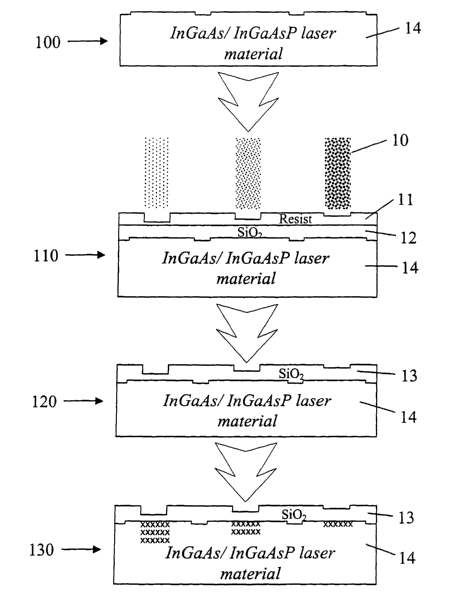
As shown in Figures 4 and 5, the gray scale mask
technique makes use of different transparency of areas of
a gray scale mask 10 to control the degree of the exposure
of photoresist 11 in selected regions and thus different
thickness of photoresist after development. The degree of
the development of photoresist 11, ie the depth of the
remaining photoresist, after the UV exposure has a linear
relationship with the optical density. In this example,
the gray scale mask 10 was designed to have 10 different
levels for multiple wavelength lasers, ie from 0.15 to 1.05
with a step of 0.1 of optical density (OD). This is shown
in Table 1 below. The stripes are of 50 ~.m width with 350
~.m spacing. Therefore it is expected to obtain 10
different bandgaps across the sample after QWI. As will be
described in detail below, for the fabrication of SLDs with
CA 02398359 2002-07-24
WO 01/67497 PCT/GBO1/00904
13
50 ~,m active windows, a 1 ~.m resolution of OD increment
from 0.15 to 1.05 was designed to produce "trapezoidal" and
"triangular" profiles, (these are illustrated, in Figure
10) .
The gray scale masks 10 are manufactured using a high-
energy beam-sensitive (HEBS) glass article of the type
described in detail in US Patent 5,078,771.
The relationship between the OD of the mask and the UV
light transmittance level (T) during lithography process
can be expressed using the following equation:
OD=-log (T)
Table 1
Gray
Level
1 2 3 4 5 6 7 8 9 10
OD 0.15 0.25 0.35 0.45 0.55 0.65 0.75 0.85 0.95 1.05
T(%) 70.8 56.2 44.7 35.5 28.2 22.4 17.8 14.1 11.2 8.9
A reactive-ion etching (RIE) process with
substantially a 1:1 selectivity between photoresist and
Si02 was then used to transfer the variable thickness
profile of the photoresist to the SiO~ layer 12 to obtain
an implantation mask 13. This process was carried out in
a conventional parallel plates RF RIE system using CF9 and
02 as process gases. Taguchi's optimization approach, a
statistical method used in industrial process optimization,
was employed to optimise the parameters of this process.
The process flow chart for the fabrication of the
multiple wavelength lasers is shown in more detail in
Figure 6. A total of four levels of masks are used in the
fabrication of this device. The first mask is used for
alignment marks and laser isolation etching (a 20 ~,m stripe
pattern). The second mask is a gray scale mask which has
an 80 ~,m width of stripe pattern. The third mask is used
for active contact window (a 50 ~,m stripe pattern) and the
CA 02398359 2002-07-24
WO 01/67497 PCT/GBO1/00904
14
last mask is to define the metal isolation (a 20 ~.m stripe
pattern).
Alignment marks and isolation stripes were first
defined (step 100) by wet-etching, using H~SOQ . H202 . H20
in 1: 8:40 ratio, to remove 0.15 ~,m of the InGaAs and
InGaAsP contact layers of the substrate 14. The sample was
coated with Si02 12 to a thickness of 0.95 ~,m after wet
etching (step 110). Then, positive photoresist 11 was
spin-coated at 3300 rpm for 35 seconds to a depth of 1.19
ZO ~m and a photolithography step was carried out to transfer
the gray scale patterns 10 onto the sample. RIE was then
performed (step 120) to transfer the graded photoresist
pattern into the Si02 mask 12 such that different thickness
of SiO~ were formed across the sample to create an
implantation mask 13.
The thickness of the photoresist 11 and SiOa
implantation mask 13, as measured from a surface profiler,
both before and after RTE for the sample is given in Figure
7.
After preparing the graded SiO~ pattern, the sample
was implanted (step 130) at 200°C with a dose of 1x1014 cm z.
The QWI step was then carried out using an RTP at 590°C for
120 seconds with the Si02 implantation mask 13 intact. The
Si02 implantation mask 13 was removed after QWI.
After fabrication, individual lasers were cleaved from
the rows of multiple wavelength lasers for light intensity
versus current and spectrum measurements. The schematic
diagram of the monolithic multiple wavelength laser 20 is
shown in Figure 8 (only 4 channels are shown in the
figure). In the example, a total of 10-channels monolithic
multiple wavelength lasers were fabricated. Each
individual laser 21 has a dimension of 400 x 500 ~m and 50
~,m width of active window, 500 ~,m cavity length and 20 ~m
width of isolation trench 22. Each laser 21 was pumped
individually during the characterization and measurements.
As shown in Figure 9, 10 distinctive wavelengths of
1.557 ~,m, 1.555 ~.m, 1.550 Vim, 1.548 ~.m, 1.543 ~,m, 1.530 Vim,
CA 02398359 2002-07-24
WO 01/67497 PCT/GBO1/00904
1.514 ~.m, 1.487 Vim, 1.479 ~.m and 1.474 ~.m, respectively,
were detected from the 10 monolithic lasers 21 that were
fabricated.
A linear correlation between thickness of the SiOz
5 implantation mask 13 and the wavelength emission was found
in Figure 7. As a result, this phenomenon has further
verified the linear relationship between the degree of
point defects generated with different thickness of Si02
implantation mask and the degree of intermixing or bandgap
10 tuning.
A superluminescent diode (SLD) has the characteristics
of high output power and low beam divergence, which are
similar to the characteristics of an injection laser diode
(LD). It gives a broad emission spectrum and low coherent
15 length, which are similar to a LED. The applications of
such device are not only limited to short and medium
distance communication systems, but also a key element in
the interferometric fiber-optic gyroscope (IFOG) system and
other fiber-optic based sensing systems. SLD has the
desirable characteristics such as the elimination of modal
noise in fiber systems, immunity to optical feedback noise,
and high coupling efficiency into fibers. As the spectral
width broadens, the coherent length is reduced. The
broadband characteristics of SLDs reduce Rayleigh
backscattering noise, polarization noise and the bias
offset due to the non-linear Kerr effect in fiber gyro
systems. Therefore, SLD offers an advantage in obtaining
the ultimate sensitivity in those applications.
Tn the following example, the same InGaAs/InGaAsP QW
structures 14 were used in the fabrication of SLDs in which
the bandgap in the SLD chip is tuned by utilizing
"triangular" and "trapezoidal" gray scale patterns to
achieve broadband luminescence from the SLD.
To obtain high output power from an SLD, one requires
a very high optical gain within the device, consequently
suppression of the lasing mode is a key concern. The
suppression techniques can be divided into two categories.
CA 02398359 2002-07-24
WO 01/67497 PCT/GBO1/00904
16
The first one is an active suppression method which
consists of using umpumped absorber, short-circuited
absorber and bending waveguide approaches. The second one
is a passive suppression method which involves using non-
absorbing window, angled-stripe and antireflection coating
(AR) approaches. The combination of an active region with
an unpumped absorbing region was applied in this example
since this method has previously been successfully
demonstrated to produce high performance SLDs.
The process flow for the fabrication of SLDs is shown
in Figure 10. A total of three levels of masks were used
in this fabrication. The first mask is used for the
definition of alignment marks. The second mask is the gray
scale mask 10 to create triangular and trapezoidal profiles
30, 31 (see Figure 6). The third mask is used to define
the active contact window 41 and the absorber section 42 (a
50 ~.m stripe pattern for active section). The alignment
marks were first defined by wet-etching the materials down
to the third epitaxial layer, the InP-upper cladding, using
chemical solutions. After the etching process, the sample
was coated with Si02 12 with a thickness of 0.95 ~Cm, and a
layer of photoresist 11 spun at 3300 rpm for 35 seconds to
a depth of 1.18 Vim. The structure was then exposed to W
through the gray scale mask 10 for a period of 5.1 seconds
(steps 200) .
After obtaining the exposed resist pattern, RIE (step
210) was then carried out to transfer the resist pattern
into the SiO2to form an implantation mask 13.
After preparing the graded Si02 patterns 13, the
samples were implanted (step 220) at 200°C with a dose of
1x1014 cm's for P impurities . The QWI step was then carried
out at 590°C for 120 seconds with the Si02 implantation
mask intact. After this, the Si02 implantation mask was
removed.
A schematic diagram of a fabricated discrete SLD 40 is
shown in Figure 11. It is noted that the absorbing section
region 42 which was not intermixed but annealed was
CA 02398359 2002-07-24
WO 01/67497 PCT/GBO1/00904
17
unpumped with no metal contact on the surface. The SLD
samples were then cleaved in order to assess their
characteristics.
Figure 12 shows the normalized emission spectra from
the two types of SLDs fabricated under the same pumping
current of 2.5 A. In general, the triangular-profiled SLD
has a wider spectrum as compared to the trapezoidal
profiled SLD.