Note: Descriptions are shown in the official language in which they were submitted.
CA 02398504 2002-07-23
WO 01/59539 PCT/US01/03288
LOW POWER MODE AND FEEDBACK ARRANGEMENT
FOR A SWITCHING POWER CONVERTER
Background of the Invention
The invention relates to the field of switching power converters and
amplifiers.
More particularly, the invention relates to switching power converters and
amplifiers
having a low power mode for conserving power.
In a conventional switching-mode power converter, a current from a power
source, such as an unregulated supply, passes through an inductor when a main
power
I O switch is closed. This charges the inductor with energy. When the switch
is opened,
the energy is discharged into a capacitor. This forms an output voltage across
the
capacitor which may then be used for driving a load. This output voltage is
maintained
at a constant, desired level by appropriately controlling the opening and
closing of the
switch, such as by pulse-width modulation (PWM) or frequency modulation.
In accordance with PWM, the duty-cycle for opening and closing the main
power switch is controlled. For example, a periodic ramp signal is compared to
a
variable signal to control the duty cycle of the switch. A level of power
delivered to the
load depends upon a duty cycle of the main power switch.
In accordance with frequency modulation, the frequency at which the main
power switch is opened and closed is controlled. For example, a voltage-
controlled
oscillator (VCO) can be utilized for controlling the main power switch. A
level of
power delivered to the load depends upon the switching frequency.
A conventional switching power amplifier is a type of switching power
converter in which the output is varied in response to an input signal. This
is in
contrast to a switching power converter in which the output is typically
maintained at a
constant level. In a typical switching power amplifier, the opening and
closing of the
main power switch is controlled in response to a level of the input signal.
Therefore,
the output of the switching amplifier tends to follow the input signal.
A class D audio amplifier is an example of a conventional type of switching
power amplifier which provides a differential output signal across a speaker
using an
H-bridge arrangement of four main power switches. Each pair of the switches is
coupled serially between a high potential of a power supply and a low
potential. Nodes
intermediate to each pair of power switches are connected to opposite
terminals of the
CA 02398504 2002-07-23
WO 01/59539 PCT/USO1/03288
speaker. By controlling the opening and closing of the four main power
switches in
accordance with an input audio signal, the audio speaker generates sounds
related to the
input signal. Because the output signal is differential, such an amplifier is
typically
operated in open loop (i.e. without feedback). A drawback to open loop
operation of
such an amplifier is that the output signal is susceptible to distortion.
Conventional switching power converters tend to provide efficiency advantages
over other types of devices. This is because switching power converters tend
to draw
power at a rate commensurate with the requirements of the load and tend to
have
relatively low energy losses. Energy loss in a switching power converter is
typically
referred to a switching loss and is largely due to energy dissipation in the
main power
switches) and in the reactive elements, such as inductors or capacitors. When
a load
consumes a level of power which is near the maximum capacity of the switching
power
converter, the switching losses are low in comparison to the total power drawn
by the
switching power converter. Thus, the converter operates with high efficiency.
As the
level of power consumed by the load decreases, however, switching losses
become
more significant in comparison to the level of power drawn from the power
supply.
Thus, at low levels of load power consumption, switching losses can
significantly
reduce efficiency. Efficiency, however, is often an important performance
criteria for a
switching power converter. For example, where the power is drawn from a
battery
supply, such as in a portable telephone, low efficiency results in reduced
periods of
operation between battery charges. Therefore, conventional switching power
converters tend make inefficient use of battery power when a load draws a low
level of
power.
Therefore, what is needed is a switching power converter which does not suffer
from the aforementioned drawbacks. It is to these ends that the present
invention is
directed.
Summary of the Invention
The present invention is a low power mode and feedback arrangement for a
switching power converter. Two or more main power switches, such as
transistors,
transfer energy from a supply to load by their opening and closing. When the
load
requires a relatively low power level, this condition is detected. In
response, one or
more of the transistor switches is disabled from switching and the reduced
power
2
CA 02398504 2002-07-23
WO 01/59539 PCT/USO1/03288
requirements of the load are handled by the remaining one or more transistor
switches.
As a result, switching losses are reduced. This is because parasitic gate
capacitance and
on-resistance associated with the disabled switches no longer consume power
from the
power source. The invention provides significant efficiency advantages during
periods
when the load draws a low level of power. This is especially useful for
battery-
powered devices which may operate in a low power mode for extended periods of
time,
such as standby mode as in a portable telephone. The prevention of power loss
may
contribute considerably to operating time before battery re-charging is
needed.
However, when additional power is required, one or more previously disabled
switches
may be brought back into operation to ensure that the power requirements of
the load
are met.
In an audio amplifier having a H-bridge arrangement for providing a
differential
output signal, the invention also provides a feedback path from only one side
of the
load. This reduces distortion associated with open-ended operation.
In accordance with one aspect of the present invention, a switching power
converter is provided having first and second transistor switches. Energy is
transferred
from a supply to a load by opening and closing the first transistor switch;
energy is
transferred from the supply to the load by opening and closing the second
transistor
switch; and the second transistor is disabled from switching upon detection of
a low
power condition.
The first switch may transfer energy from the supply to a first reactive
element
upon closing and the first switch may transfer energy from the first reactive
element to
a second reactive element upon opening. The second transistor switch may
transfer
energy from the supply to a third reactive element upon closing and the second
transistor switch may transfer energy from the third reactive element to the
second
reactive element upon opening. Switching ofthe first and second transistor
switches
may be interleaved. The first and second transistor switches may be coupled in
parallel
to each other. Switching of the first transistor switch may be synchronized
with
switching of the second transistor switch when the second transistor switch is
actively
switching. The first transistor switch may be disabled from switching when the
second
transistor switch is actively switching. The switching power converter may
include a
pulse-width modulation switch controller coupled to the first and second
switches. The
switching power converter may include a frequency modulation switch controller
CA 02398504 2002-07-23
WO 01/59539 PCT/USO1/03288
coupled to the first and second switches. The low power detector may detect
the low
power condition by monitoring a voltage provided to the load or by monitoring
an error
signal representative of a difference between a voltage provided to the load
and a
desired level for the voltage. The low power detector may include a comparator
having
a hysteretic transfer characteristic. The first and second transistor switches
may have
substantially different current-carrying capacities. Energy may be transferred
to the
load by a current which is synchronously rectified. The switching power
converter may
also include a third transistor switch and a fourth transistor switch, the
third and fourth
transistor switches for performing synchronous rectification on the current,
wherein the
fourth transistor is disabled by the low power detector upon detection ofthe
low power
condition.
In accordance with a further aspect of the invention, a switching power
converter is provided which includes a switch controller and a plurality of
transistor
switches including a first transistor switch and a group of at least two
additional
transistor switches. Each transistor switch is coupled to the switch
controller for
transferring power from a supply to a load by the switch controller opening
and closing
the corresponding transistor switch. A low power detector is coupled to the
group of at
least two additional transistor switches for selectively disabling switching
of one or
more of the transistor switches of the group in accordance with a detected
level of
power provided to the load.
The plurality of transistor switches may be coupled in parallel to each other.
The transistor switches of the plurality that are actively switching may be
synchronized.
The switch controller may be a pulse-width modulation switch controller. The
switch
controller may be a frequency modulation switch controller. The low power
detector
may detect the level of power provided to the load by monitoring a voltage
provided to
the load or by monitoring an error signal representative of a difference
between a
voltage provided to the load and a desired level for the voltage. The low
power
detector may include a comparator having a hysteretic transfer characteristic.
In accordance with another aspect of the invention, a switching amplifier is
provided for receiving an input signal and for generating and output signal
representative of the input signal. A first pair of transistor switches
alternately raises
and lowers a voltage potential of a first terminal of a reactive element upon
switching
of the first pair of transistor switches; a second pair of transistor switches
alternately
4
CA 02398504 2002-07-23
WO 01/59539 PCT/USO1/03288
raises and lowers a voltage potential of the first terminal of the reactive
element upon
switching of the second pair of transistor switches; a switch controller
controls
switching of the first and second pairs of transistor switches in accordance
with the
input signal for forming the output signal at a second terminal of the
reactive element.
A low signal level detector is coupled to the second pair of transistor
switches for
disabling the second pair of transistor switches from switching upon detection
of a low
input signal level condition.
The input signal may be an audio signal. The switching amplifier may include a
speaker coupled to receive output signal. The switching amplifier may include
one or
more additional pairs of transistor switches for alternately raising and
lowering a
voltage potential ofthe first terminal ofthe reactive element, each additional
pair being
selectively disabled by the low signal level detector upon detection of a
corresponding
low signal level condition. The transistor switches of the first pair may have
substantially equal current carrying capacities which are substantially
different from
current carrying capacities of the transistor switches of the second pair. The
low signal
level detector may detect the low power condition by monitoring the input
signal or by
monitoring an error signal representative of a difference between the input
signal and a
reference level. The low power detector may include a window comparator. The
window comparator may have a hysteretic transfer characteristic. The switching
amplifier may include a feedback path from a terminal of the reactive element
to the
switch controller for limiting the output signal. The first pair of transistor
switches may
be actively switching when the low signal level condition is not detected. The
first pair
of transistor switches may be disabled by the low signal level detector when
the low
signal level condition is not detected.
In accordance with yet another aspect of the invention, a switching amplifier
is
provided for receiving an input signal and for generating a differential
output signal
representative of the input signal. A first pair of transistor switches
alternately raises
and lowers a voltage potential of a first terminal of a first reactive element
upon
switching of the first pair of transistor switches; a second pair of
transistor switches
alternately raises and lowers a voltage potential of the first terminal of the
first reactive
element upon switching of the second pair of transistor switches; a third pair
of
transistor switches alternately raises and lowers a voltage potential of a
first terminal of
a second reactive element upon switching of the third pair of transistor
switches; and a
5
CA 02398504 2002-07-23
WO 01/59539 PCT/USO1/03288
fourth pair of transistor switches alternately raises and lowers a voltage
potential of the
first terminal of the second reactive element upon switching of the fourth
pair of
transistor switches. A switch controller controls switching of the first,
second, third
and fourth pairs of transistor switches in accordance with the input signal
for forming a
differential output signal across a second terminal of the first reactive
element and a
second terminal of the second reactive element. A low signal level detector is
coupled
to the second and fourth pair of transistor switches for disabling the second
and fourth
pair of transistor switches from switching upon detection of a low input
signal level
condition.
The input signal may be an audio signal. The switching amplifier may include a
speaker coupled to receive the differential output signal. The switching
amplifier may
include one or more additional pairs of transistor switches for alternately
raising and
lowering a voltage potential of the first terminal of the reactive element,
and one or
more additional pairs of transistor switches for alternately raising and
lowering a
voltage potential of the first terminal of the second reactive element, each
additional
pair being selectively disabled by the low signal level detector upon
detection of a
corresponding low signal level condition. The transistor switches of the first
pair may
have substantially equal current carrying capacities which are substantially
different
from current carrying capacities of the transistor switches of the second
pair. The low
signal level detector may be detected the low signal level condition by
monitoring the
input signal or by monitoring an error signal representative of a difference
between the
input signal and a reference level. The low power detector may include a
window
comparator. The window comparator may have a hysteretic transfer
characteristic.
The switching amplifier may include a feedback path from a terminal of the
first
reactive element to the switch controller for limiting the differential output
signal. A
corresponding feedback path from the second reactive element to the switch
controller
may not be present. The first and third pairs of transistor switches may be
actively
switching when the low input signal level condition is not detected. The first
and third
pairs of transistor switches may be disabled by the low signal level detector
when the
low input signal level condition is not detected. The switching amplifier may
be
implemented in an eight pin integrated circuit package.
In accordance with a further aspect of the present invention, a switching
amplifier is provided for receiving an input signal and for generating a
differential
CA 02398504 2002-07-23
WO 01/59539 PCT/USO1/03288
output signal representative of the input signal. A first pair of transistor
switches
alternately raises and lowers a voltage potential of a first terminal of a
first reactive
element upon switching of the first pair of transistor switches; a second pair
of
transistor switches alternately raises and lowers a voltage potential of a
first terminal of
a second reactive element upon switching of the second pair of transistor
switches; and
a switch controller controls switching of the first and second pairs of
transistor switches
in accordance with the input signal for forming a differential output signal
across a
second terminal of the first reactive element and a second terminal of the
second
reactive element. A feedback path is provided from a terminal of the first
reactive
element to the switch controller for limiting the differential output signal.
A
corresponding feedback path from the second reactive element to the switch
controller
may not be present.
Brief Description of the Drawings
Figure 1 illustrates a schematic diagram of a switching power converter having
a low power mode in accordance with the present invention;
Figures 2A-C illustrate timing diagrams for selected signals of the power
converter illustrated in Figure 1;
Figure 3 illustrates a first alternate embodiment of the power converter of
Figure 1 in which synchronous rectification is performed;
Figure 4 illustrates a second alternate embodiment of the power converter of
Figure 1 in which parallel paths are provided for charging the output node;
Figures 5A-C illustrate timing diagrams for selected signals ofthe power
converter illustrated in Figure 4;
Figure 6 illustrates a schematic diagram of a low power detection circuit for
the
power converter of Figure l;
Figure 7 illustrates a schematic diagram of a switching power amplifier having
a
low power mode and feedback arrangement;
Figure 8 illustrates a schematic diagram of a low power detection circuit for
the
power amplifier of Figure 7; and
Figure 7 illustrates a schematic diagram of a class D switching power
amplifier
having a feedback arrangement and low power mode.
7
CA 02398504 2002-07-23
WO 01/59539 PCT/USO1/03288
Detailed Description of a Preferred Embodiment
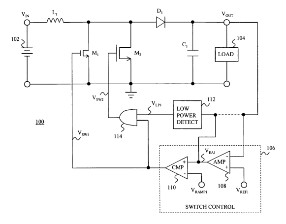
Figure 1 illustrates a schematic diagram of a switching power converter 100
having a low power mode in accordance with the present invention. The power
converter 100 is coupled to receive power from a power supply 102. The supply
102
may be, for example, an unregulated direct-current (DC) supply, such as a
battery or a
rectified alternating current (AC) signal. The supply 102 forms a voltage V,N
which
may be coupled to a first terminal of a reactive element, such as an inductor
L,. A
second terminal of the inductor L, may be coupled to a drain terminal of an n-
type
field-effect transistor M~, to a drain terminal of an n-type field-effect
transistor MZ and
to an anode of a diode D,. A cathode of the diode D, may be coupled to a first
terminal
of a reactive element, such as a capacitor C,, and to a first terminal of a
load 104.
Source terminals of the transistors M, and M2, a second terminal of the
capacitor C,
and a second terminal of the load 104 may be coupled to a ground node. Because
the
drain and source terminals of the transistors M, and MZ are coupled together,
the
transistors M, and MZ may be said to be coupled in parallel.
The transistors M, and MZ may function as switches. Activating (closing) one
or both of the transistor switches M, and MZ by turning the transistors M, and
M~ on
results in a current which passes through the indictor Li. This transfers
energy from the
supply 102 to an electromagnetic field associated with the inductor L,. When
the
transistors M, and M~ are deactivated (opened) by turning the transistors M,
and Mz
off, energy stored by the inductor L, is transferred to the capacitor C,. By
repeatedly
opening and closing one or both of the transistor switches M, and Mz, an
output voltage
Vou~ is built up across the capacitor C,. The output voltage VouT is available
for
providing power to the load 104.
A switch controller 106 may control the transistor switches M~ and MZ based
upon a level of the output voltage VouT. The switch controller 106 may include
an
amplifier 108 and a comparator 110. An inverting input of the amplifier 108
may be
coupled to receive the output voltage VouT. A resistive voltage divider (not
shown)
may be coupled to the inverting input of the amplifier 108 for stepping down
the output
voltage VouT. A reference voltage VRrFi may be coupled to a non-inverting
input of the
amplifier 108. The reference voltage VREF, corresponds to a desired level for
the
output voltage VouT. Accordingly, the output of the amplifier 108 forms an
error signal
VEA, which is representative of a difference between the output voltage VouT
(or a
8
CA 02398504 2002-07-23
WO 01/59539 PCT/1JS01/03288
portion of VouT from the resistive voltage divider) and a desired level for
the output
voltage VouT. This error signal VEA, may be coupled to a non-inverting input
of the
comparator 110 while a periodic ramp signal VRannhl may be coupled to an
inverting
input of the comparator 1 10. The output of the comparator 1 10 forms a switch
control
S signal Vsw, which may be coupled to the gate of the transistor switch M, for
controlling the transistor switch MI.
Figure 2A illustrates a timing diagram for the signals VFaI and VRnMPI. As
shown in Figure 2A, the error signal VEAi varies in response to changes the
output
voltage Vou~,~. While the output voltage VouT is regulated to a desired level,
it may
undergo transient variations. For example, the output voltage VouT may vary in
response to changes in a level of current drawn by the load 104. As is also
shown in
Figure 2A, the ramp signal VRaMPI has a approximately constant slope over each
of it
periods. The ramp signal VRAMr~I is reset to an initial value at the end of
each period.
The ramp signal VRnMI>i may be generated by conventional circuitry.
Figure 2B illustrates a timing diagram for the switch control signal VsW,.
Note
that Figure 2B is drawn with a time scale along the horizontal axis which is
equivalent
to that of Figure 2A. As shown in Figure 2B, the switch control signal VsWI
may be a
logical high voltage, causing the transistor switch M, to close, at times when
the ramp
Slgnal VRAMP IS lower than the error signal VEAI. As is also shown in Figure
2B, the
signal Vsw, may be a logical high voltage, causing the transistor switch M, to
open, at
times when the ramp signal VRnMh is higher than the error signal Vr,A,.
Accordingly, as
shown in Figure 2B, a duty-cycle for the transistor switch M, may vary with
changes in
the error signal VEAI so as to regulate VouT at the desired level.
It will be apparent that the switch controller 106 of Figure 1 is a
conventional
PWM switch controller. Because the closing of the transistor switch M,
coincides with
the resetting ofthe ramp Slgnal VRAMPI, the switch controller 106 may be
considered to
perform trailing edge modulation. It will be apparent that the switch
controller 106
may be altered or replaced by another type of switch controller. For example,
the
switch controller 106 may be modified to perform leading edge modulation. This
may
be accomplished, for example, by reversing the polarities of the inputs to the
amplifier
108 and the comparator 1 10. As another example, the switch controller 106 may
be
replaced by a frequency modulation switch controller.
9
CA 02398504 2002-07-23
WO 01/59539 PCT/USO1/03288
Referring Figure 1, a low power detector 112 may also be coupled to monitor
the error signal VET,. Alternately, the low power detector 1 12 may be coupled
to
monitor the output voltage Vo~~. This is shown in Figure I by a dotted line
between
the input of the amplifier 108 and the input of the low power detector 1 12.
Assuming
the detector 112 is coupled to the input of the amplifier 108, then the
detector I 12 need
not be coupled to the output of the amplifier 108. An output of the low power
detector
112 forms a signal V~p, which may be coupled to a first input of a logic AND
gate 114.
The switch control signal Vsw, may be coupled to a second input of the logic
AND gate
114. An output of the logic AND gate 114 forms a switch control signal VsW2
which
may be coupled to the gate of the transistor switch MZ for controlling the
transistor
switch MZ. Figure 2C illustrates a timing diagram for the switch control
signal VsWZ,
while Figure 2D illustrates a timing diagram for the low power detection
signal V~r,
formed by the low power detector 1 12. Note that Figures 2C-D are drawn with a
time
scale which coincides with that of Figures 2A-B. When the signal V~r, is logic
high
voltage, the switch control signal Vsw, is passed by the logic AND gate 1 14.
Under
such circumstances, the transistor switch MZ may be synchronized with the
transistor
switch M, and may operate in accordance with the same duty cycle, as shown by
comparing Figures 2B and 2C prior to a time T, and after a time T4.
However, when the low power detector 112 detects that the load 104 draws a
relatively light load, the low power detection signal VLP, may transition from
a logic
high voltage to a logic low voltage. This is shown occurring in Figure 2D
sometime
after the time T, and before the time Tz. In response to this transition in
the signal
V~,>,, the logic AND gate 1 14 inhibits the switch control signal VsW, from
passing to its
output. Instead, the signal VsW2 formed at the output of the logic AND gate 1
14 is held
at a logic low voltage. This is shown in Figure 2C at the time TZ where the
signal VsW
remains a logic low voltage, whereas, the signal VsW, transitions from a logic
low
voltage to a logic high voltage. Accordingly, the transistor switch Mz is
disabled upon
detection of a low power condition. Assuming a low power condition is no
longer
detected, then the signal V~p, may transition back to a logical high voltage,
as shown
occurring in Figure 2D after a time T3 and before the time T4. As a result,
the transistor
switch Mz is enabled to resume switching in concert with the transistor switch
M,, as
shown occurring in Figure 2D at the time T4.
CA 02398504 2002-07-23
WO 01/59539 PCT/USO1/03288
This feature of the present invention may provide significant efficiency
benefits
when the power requirements ofthe load 104 change significantly over time. For
example, the load 104 may be a battery-powered device, such as a portable
telephone.
When the telephone is in use, such as for making a telephone call, then its
receiver and
transmitter may both be active. Under these circumstances, both the transistor
switches
M, and M~ may be actively switching to supply sufficient power to the
telephone.
When the call ends, the telephone may enter a standby mode in which the
receiver is
active, but the transmitter is inactive. As a result, less power is drawn by
the telephone.
This may cause the output voltage Vo~~~ supplied to the telephone to increase
somewhat
and, thus, the level of error signal VEA, may fall. Note that when the load
104 draws a
low level of power, the output voltage Vo«T tends to rise due to opening and
closing of
the switches M~ and M~. This is because even at a minimum duty-cycle,
switching may
still occur. As a result, the low power detector 1 12 may detect that the
telephone is in a
low power mode and, in response, disables switching of the transistor switch
M~.
Switching of the switch M,, by itself, may then provide sufficient power for
the
portable telephone when it is in standby mode. When the portable telephone is
again
used for a telephone call, then its transmitter may be activated. This may
cause the
output voltage Vo~~- to fall somewhat and, thus, the error signal VIA, may
rise. As a
result, the low power detector 104 may detect that the telephone is in a high
power
mode and, in response, re-enables switching ofthe transistor switch Mz.
Switching losses in the transistor switches M, and M~ are largely a result of
parasitic capacitance at their gates. This parasitic gate capacitance is
charged and then
discharged each time the corresponding transistor is activated and then
deactivated.
The gate capacitance of a transistor is related to the size of the current-
carrying channel
2~ of the transistor. For a small transistor which has a small current-
carrying capacity, the
gate capacitance tends to be relatively small. In contrast, for a large
transistor which
has a large current-carrying capacity, the gate capacitance tends to
relatively large.
Because the transistor switch MZ is disabled during periods of low power
consumption,
switching losses associated with the switch MZ are essentially eliminated
during such
periods. While switching losses are associated with the transistor M~ during
low power
mode operation, these switching losses may less than would be the case for a
single
transistor which had current capacity for worst-case power requirements of the
Load
104. In accordance with the present invention, the transistor switch MZ is
brought into
CA 02398504 2002-07-23
WO 01/59539 PCT/US01/03288
play only as necessary, such as when needed to satisfy the power requirements
of the
load 104. -
In the preferred embodiment, the transistor switches M, and MZ are sized so as
to correspond with the various power requirements of the load 104. Considering
the
portable telephone example, power consumed in the standby mode can be expected
to
be less than approximately one-fourth of the power consumed when the telephone
is
being used during a telephone call. Accordingly, the transistor M, may have a
substantially smaller current carrying capacity than the transistor M~. For
other loads,
the proportions of power consumed in different operating modes may differ. For
example, assume a load operates one of two modes where the power consumed in a
first mode is approximately eighty percent of the power consumed in a second
mode.
For such a load, the transistor M, may have a substantially greater current
carrying
capacity than the transistor M~. For other loads, the transistors M, and Mz
may have
substantially equal current-carrying capacities. In addition to loads which
draw power
at relatively discrete levels, the invention may also provide efficiency
advantages for
loads which draw continuously varying levels of power.
Further, in addition to providing a single transistor which may be selectively
disabled, such as the transistor M~ (Figure 1), it will be apparent that one
or more
transistors may be provided, one or more of which may be selectively disabled
depending upon the level of power consumed by the load. For example, for a
load
which operates primarily in three distinct modes, each having a corresponding
level of
power consumption, a power converter may be provided for powering the load
with
three transistors switches having appropriate current-carrying capacity, one
or two of
which are selectively disabled depending upon the level of power consumed by
the
load. The low power detector 1 12 may then provide multiple outputs to specify
one of
a plurality of such low power modes. It will be apparent also that by
appropriately
modifying the logic circuitry of Figure l, the transistor M, may be disabled
from
switching when the transistor MZ is actively switching.
The diode D, of Figure 1 performs signal rectification such that current flows
from the inductor L, for charging the capacitor Ci, however, current is
prevented by the
diode D, from discharging the capacitor C~ through the transistor switches M~
and Mz.
Figure 3 illustrates an alternate embodiment of the power converter 100 of
Figure 1 in
which synchronous rectification is performed. More particularly, the diode D,
of
12
CA 02398504 2002-07-23
WO 01/59539 PCT/USO1/03288
Figure 1 is replaced by n-type transistors M3 and M~. The transistor M3
receives the
switch control signal VsW,, while the transistor M~ receives a switch control
signal
VsW3. The switch control signal Vswi is coupled to a first input of an
inverter 116. An
output of the inverter 116 is coupled to a first input of a logic AND gate
118. A second
input ofthe logic AND gate 118 is coupled to receive the signal Vr~~ from the
low
power detector 1 12. An output of the logic AND gate 118 is coupled to an
input of an
inverter 120. An output of the inverter 120 forms the switch control signal
Vsw3 which
is coupled to the gate of the transistor M4.
Under normal operating conditions, the transistor switch M3 is open when the
transistor switch M, is closed and vice versa. Similarly, the transistor
switch M,~ is
open when the transistor switch M~ is closed and vice versa. Accordingly,
during
normal operation, the transistor switches M3 and M~ operate synchronously with
the
transistor switches M, and M~ to rectify the current flowing to the capacitor
C~ from the
inductor L,. It will be understood, that the controller 106' preferably
includes make-
before-break circuitry (not shown) which ensures that the transistors M i and
M3 are not
both turned on at the same time. Similarly, the controller 106" preferably
ensures that
the transistor switches M~ and M4 are not both turned on at the same time.
In the low power mode, when the signal Vr,~, is logic low voltage, the
transistor
switches MZ and M4 are disabled from switching. Under such conditions, each
transistor switch Mz and Ma is turned off.
The transistor switches M3 and M4 are preferably sized substantially the same
as
the corresponding transistor switches M~ and Mz, respectively. Synchronous
rectification may also be accomplished by omitting the transistor Mz and
sizing the
transistor M, appropriately to carry all of the current from the inductor L,
to the
capacitor Ci.
Figure 4 illustrates a second alternate embodiment of the power converter of
Figure 1 in which parallel paths are provided for delivering power to the load
104. The
power converter 100" of Figure 4 differs from that of Figure 1 in that a
second inductor
L~ provides a second path through which the capacitor C~ may be charged from
the
input supply V,N. Current through the second inductor LZ is controlled by the
transistor
switch M2. Accordingly, the input supply V,N is coupled to a first terminal of
the
inductor L~. A second terminal of the inductor Lz is coupled to the drain of
the
13
CA 02398504 2002-07-23
WO 01/59539 PCT/USO1/03288
transistor switch MZ and to an anode of a diode D2. A cathode of the diode Dz
is
coupled the first terminal of the capacitor C~.
Under normal operating conditions, the transistor switches M, and MZ (Figure
4) are both switching so that each provides a portion of the power delivered
to the load
104. In the preferred embodiment, the transistor switches Mi and MZ are
operated in an
interleaved fashion. Thus, the switch M, is cycled from closed-to-open-to-
closed while
the switch MZ remains closed. Similarly, the switch MZ is cycled from closed-
to-open-
to-closed while the switch Mi remains closed. Figures SA-C illustrate timing
diagrams
for selected signals of the power converter illustrated in Figure 4. The
transistor
switches M, and M~ of Figure 4 are controlled by switch control signals VsW~'
and
VsW2', respectively.
As can be seen from Figures 5A-SD, when the output VL~~ of the low power
detector 1 12 is a logic high voltage, the transistor switches Mi and M~ are
both actively
switching in an interleaved fashion. When the low power detector 1 12 detects
a low
power condition, however, the signal V~ri transitions to a logic low voltage.
As shown
in Figures 5C-5D, this disables the transistor switch Mz from switching until
the signal
V~,~i returns to a logic high voltage.
The switch controller 106' of Figure 4 differs from that of Figure 1 in that a
flip-flop 122 and logic AND gates 124 and 126 provide the switch control
signals
Vsw,' and VsW2'. More particularly, a clock signal V~~K may be coupled to a
toggle
input of the flip-flop 122. Preferably, the flip-flop 122 is leading edge
triggered while
leading edges of the clock signal V~~K correspond with resetting of the ramp
signal
VRAMm, as shown in Figure SA. Thus, a Q output ofthe flip-flop 122 provides
square
wave signal of one-half the frequency of the clock signal V~~K and is coupled
to a first
input of the logic AND gate 126. An inverted output Q of the flip-flop 122 is
coupled
to a first input of the AND gate 124. A second input of each AND gate 124 and
126 is
coupled to receive an output signal VcM,~ from the comparator 1 10. The logic
AND
gate 124 provides the switch control signal VsW,' for controlling the switch
M,.
Similarly, the logic AND gate 126 provides the switch control signal VsW2' for
controlling the switch M2.
The inductors L, and L~ may be of the same inductance value or may be of
different values. In the preferred embodiment, the inductors Li and LZ have
inductance
values which correspond to the sizes of the transistor switches M~ and MZ and
to
14
CA 02398504 2002-07-23
WO 01/59539 PCT/USO1/03288
various levels of power expected to be drawn by the load 104. Further, one or
both of
the diodes D, and Dz may be replaced by switches for performing synchronous
rectification.
Figure 6 illustrates a schematic diagram of the low power detector 1 12 of
Figure
1. A reference voltage VRerz may be coupled to a first terminal of a resistor
R,. A
second terminal ofthe resistor Ri may be coupled to a first terminal of a
resistor Rz and
to a first terminal of a comparator 128. A second terminal of the resistor Rz
may be
coupled to the ground node. The resistors R, and Rz form a resistive divider.
Accordingly, a reference voltage VRE,:3 formed at the first input of the
comparator 128
is proportional to the reference voltage V,~FZ. As mentioned, the low power
detector
I 12 may be coupled to monitor either the output voltage Vou-r or the error
signal VEAL
to determine whether a load coupled to the power converter 100 is in a low
power
mode. Assuming the error signal V~;~, is monitored, it may be coupled to a
second
input of the comparator 128. An output of the comparator 128 forms the signal
V~r~.
As mentioned, under normal operating conditions, when both of the transistor
switches Mi and Mz are operating, the signal VIP, is a logical high voltage.
When the
level of VIA, falls below the level of VREF3, this indicates that the load 104
is in a low
power mode. The comparator 128 responds by changing the signal V,_~, from a
logical
high voltage to a logical low voltage. This disables switching ofthe
transistor Mz.
Preferably, the comparator 128 has a hysteretic transfer characteristic. This
prevents
the transistor Mz from being disabled and enabled unnecessarily when the
signal VEA,
hovers about the level of the reference voltage VREF3~ Thus, the signal VL,>,
preferably
does not return to a logic high voltage until the level of VEAi rises above
the level of
uREF3 by a predetermined amount, as determined by the amount of hysteresis of
the
comparator 128.
Note that assuming more than two transistor switches are provided, the (ow
power detector 112 may include an additional comparator for each additional
transistor
switch along with appropriate other logic circuitry. Each additional
comparator may
have a first input coupled to VEp~ (or VouT), a second input coupled to an
appropriate
reference voltage level and an output coupled to enable/disable the
corresponding
transistor switch.
In sum, a switching power converter is disclosed which includes a plurality of
main power switches, at least one of which may be disabled from switching
while the
CA 02398504 2002-07-23
WO 01/59539 PCT/USO1/03288
others continue actively switching when a load powered by the converter draws
a low
level of power. Optionally, at least one transistor switch utilized for
synchronous
rectification may also be disabled in response to a low level of power. This
feature is
advantageous as it reduces switching losses and, thus, increases efficiency
for periods
of low power consumption by the load. Because the load may operate in a low
power
mode for an extended period of time, such as standby mode in a battery-powered
telephone, the prevention of power loss may contribute considerably to
operating time
before the battery re-charging is needed.
Figure 7 illustrates a schematic diagram of a switching power amplifier 200
having a low power mode and a feedback arrangement in accordance with the
present
invention. Referring to Figure 7, a supply voltage V~~ may be coupled to a
source
terminal of a p-type field-effect transistor M; and to a source terminal of an
n-type
field-effect transistor M6. A drain terminal of the transistor MS may be
coupled to a
drain terminal of the transistor M6, to a drain terminal of an n-type field-
effect
transistor M~, to a drain terminal of an n-type field-effect transistor Mg and
to a first
terminal of an inductor L3. A second terminal of the inductor L3 may be
coupled to a
first terminal of a capacitor C2. A source terminal of the transistor M~, a
source
terminal of the transistor M8 and a second terminal of the capacitor CZ may be
coupled
to a ground node.
The transistors M;-M8 may function as switches. Preferably, the pair of
transistor switches M; and M~ are operated such that when the transistor
switch M; is
activated (closed), the transistor switch M~ is deactivated (opened); and when
the
transistor switch M; is deactivated (opened), the transistor switch M~ is
activated
(closed). The pair of transistor switches M6 and Mg may be selectively
disabled from
switching. When disabled, the transistor switches M6 and M8 are both
deactivated
(opened). When actively switching, the transistor switches M6 and Mg are
preferably
operated such that the transistor switch M6 is in the same condition (opened
or closed)
as the transistor switch MS and the transistor switch Mg is in the same
condition as the
transistor switch M~. Thus, when actively switching, the pair of transistor
switches M6
and M8 are synchronized with the corresponding transistor of the pair M5 and
M~.
Accordingly, when one or both of the transistor switches M; and M6 is closed,
the transistor switches M~ and M8 are open. Under these conditions, a voltage
at the
first terminal of the inductor L3 is increased. As a result, a current from
the supply
16
CA 02398504 2002-07-23
WO 01/59539 PCT/USO1/03288
voltage V~~ tends to flow through the inductor L3 to the capacitor Cz. This
tends to
increase a voltage across the capacitor Cz. When one or both of the transistor
switches
M~ and Mg is closed, the transistor switches MS and M6 are open. Under these
conditions, the voltage at the first terminal of the inductor L3 is decreased.
As a result,
a current tends to be drawn from the capacitor Cz and through the inductor L3
to the
ground node. This tends to reduce the voltage across the capacitor Cz. The
inductor L3
and the capacitor Cz function as a smoothing filter such that a voltage formed
across the
capacitor Cz is representative of an average of the voltage at the first
terminal of the
inductor L3.
A speaker 202 may be coupled to receive an audio output signal AUDouT
formed across the capacitor C~. More particularly, a first terminal of an
inductor L4
may be coupled to the first terminal of the capacitor Cz. A second terminal of
the
inductor L4 may be coupled to a first terminal of the speaker 202. A second
terminal of
the speaker 202 may be coupled to a first terminal of a capacitor C3. A second
terminal
of the capacitor C3 may be coupled to the ground node. Alternately, the
speaker 202
may be coupled to the capacitor Cz via a transformer (not shown). In which
case, a
primary winding of the transformer may be coupled in series between the first
terminal
of the capacitor Cz and the ground node, while the speaker may be coupled
across a
secondary winding of the transformer.
A switch controller 204 may be coupled to control the switches MS-Mg for
powering a speaker 202 based upon an input audio signal AUD,N. More
particularly,
the audio input signal AUD,N may be coupled to a first terminal of a resistor
R3. A
second terminal of the resistor R3 may be coupled to the switch controller
204. The
switch controller 204 may include an amplifier 206, a comparator 208 and a
compensation capacitor Ca. An inverting input of the amplifier 206 may be
coupled to
the second terminal of the resistor R3 and to a first terminal of the
capacitor C4. A
reference voltage VREFa may be coupled to a non-inverting input of the
amplifier 206.
The reference voltage VReFn may be set to a desired quiescent level for the
audio output
signal AUDouT (e.g., Vcc~2). Thus, the switch controller 204 receives the
audio input
signal AUD,N via the resistor R3 and forms the error signal VEAZ at the output
of the
amplifier 206. The error signal VE.az is representative of a deviation in the
AUD,N
signal from the reference voltage VREF4~
I7
CA 02398504 2002-07-23
WO 01/59539 PCT/USO1/03288
The output of the amplifier 206 may be coupled to a second terminal of the
capacitor C4 and to a non-inverting input of the comparator 208. An inverting
input of
the comparator 208 may be coupled to receive a periodic ramp signal VRAMrz,
similar to
the ramp signal VRAMr~i (Figure 2A). The error signal VEAL is then compared by
the
comparator 208 to the ramp signal VRAMP2~ An output of the comparator 208
forms a
switch control signal Vsw:~ which may be coupled to a gate of the transistor
switches
M3 and M~ for controlling the transistor switches M; and M~.
Accordingly, the switch control signal Vsw:~, formed by the comparator 208, is
pulse-width modulated in accordance with the audio input signal AUD,N so as to
control the transistors M; and M~ to form the audio output signal AUDo~~,- at
the first
terminal of the capacitor C~. A resistor R~ may be coupled to provide negative
feedback, such as from the second terminal ofthe inductor L~ to the second
terminal of
the resistor R;.
A low power detector 210 may be coupled to monitor the error signal VEAL.
1 ~ Alternately, the low power detector 210 may be coupled to monitor the
audio input
signal AUD,N, as shown by the dotted line between the second terminal of the
resistor
R3 and the input of the detector 212. An output V~PZ of the low power detector
210
may be coupled to a first input terminal of a logic AND gate 212 and to a
first input
terminal of a logic AND gate 214. The switch control signal VsW~ may be
coupled to a
second input of the logic AND gate 214 and to a second input of the logic AND
gate
212 via an inverter 216. An output of the logic AND gate 212 forms a switch
control
signal Vsw; which may be coupled to the gate of the transistor switch M6 via
an
inverter 218. An output of the logic AND gate 214 forms a switch control
signal VsW~
which may be coupled to the gate of the transistor switch M8.
Thus, when the low power detection signal VLP2 is a logical high voltage, the
switch control signal Vsw~ is passed by the logic AND gate 214 to form the
switch
control signal Vsw~ and the switch control signal VsW4, as inverted by the
inverter 216,
is passed by the logic AND gate 212 to form the switch control signal VsW;.
Under
such conditions, the transistor switches M6 and Mg may actively switch in
synchronism
with the switches M; and M~, respectively. However, when the input signal
AUD,N is
relatively low in amplitude, this means that the speaker 202 requires less
power than
when the signal AUD,N is of relatively high amplitude. Accordingly, the low
power
detector 210 detects this condition by monitoring the error signal VEnz (or
the input
18
CA 02398504 2002-07-23
WO 01/59539 PCT/USO1/03288
signal AUD,N). In response, the output V~,~z of the low power detector 210 may
transition from a logic high level to a logic low level. When the signal VL~z
is a logic
low voltage, the switch control signals VsW; and VsWb are held to a logic low
level by
the AND gates 212 and 214, respectively. Under these conditions, the
transistor
switches M6 and M8 are disabled from switching.
In summary, under low audio input signal AUDiN levels, such a low volume
setting, less power is required to drive the speaker 202 than would be
required
otherwise. Accordingly, to save power, the transistors M6 and M8 are disabled
from
switching. This feature provides efficiency benefits by avoiding switching
losses
caused by the transistor switches M~, and Mg.
Figure 8 illustrates a schematic diagram of the low power detector 210 of
Figure
7. Referring to Figure 8, a reference voltage VR~r; may be coupled to a first
terminal of
a resistor R;. A reference voltage VREr~, is formed at a second terminal of
the resistor
R; and may be coupled to a first terminal of a resistor R~ and to a first
terminal of a
1 ~ comparator 220. A reference voltage VREF7 ~S formed at a second terminal
of the
resistor R6 and may be coupled to a first terminal of a resistor R~ and to a
first terminal
of a comparator 222. A second terminal of the resistor R~ may be coupled to
the
ground node. The error signal VrA~ may be coupled to a second input of the
comparator 220 and to a second input of the comparator 222. An output of the
comparator 220 may be coupled to a first input of a logic OR gate 224, while
an output
of the comparator 222 may be coupled to a second input of the logic OR gate
224. An
output of the logic OR gate 224 forms the signal V~,~z.
Together, the comparators 220 and 222 and the logic OR gate 224 form a
window comparator such that the output VLPZ is a logic high voltage, and the
transistors
M6 and M8 (Figure 7) are enabled, only when its input signal VEA? is higher
than VREF6
or lower than VREr~. When the error signal VEn2 is between the levels of VREF~
and
VRrr~, then a low power condition is indicated in which the output signal V~PZ
is a logic
low voltage and the transistor switches M6 and Mg are disabled from switching.
The
levels of V~F6 and VREF~ can be selected to adjust the thresholds at which the
low
power detector 210 indicates a low power condition. A window comparison is
preferred over a single threshold comparison because the audio input signal
AUD,N is
expected to be an alternating current (AC) signal with positive and negative
swings.
Thus, the upper threshold VREF6 of the window comparator detects positive
swings in
19
CA 02398504 2002-07-23
WO 01/59539 PCT/L1S01/03288
the audio input signal AUD,N and the lower threshold VREF~ detects negative
swings.
In the preferred embodiment, the comparators 220 and 222 each have a
hysteretic
transfer characteristic so as to avoid enabling and disabling the transistor
switches M6
and M8 excessively should the input signal VHA~ hover about one of the
threshold
voltages VREF6 Or VREF7~
It will be apparent that appropriate modifications to the logic circuitry of
Figure
7 may be made to disable transistor pair MS and M6 from switching, if desired,
when
the transistor pair M~ and Mg are actively switching. Thus, only one ofthe
pairs of
transistor switches may be actively switching at a time. It will also be
apparent that the
power amplifier 200 may be provided with additional pairs of transistor
switches which
may be selectively enabled and disabled according to the level of the input
signal
AUD,N or the error signal VEAL.
Figure 9 illustrates a schematic diagram of a class D switching power
amplifier
300 having a feedback arrangement and low power mode in accordance with the
present invention. The power amplifier 300 of Figure 9 is similar to the power
amplifier 200 illustrated in Figure 7 with important differences discussed
below.
Elements of Figure 9 having a one-to-one functional correspondence with those
of
Figure 7 are given the same reference numeral. An important difference between
the
amplifier 200 (Figure 7) and the amplifier 300 (Figure 9) is that the
amplifier 300
includes a second switching stage 304 in addition to a first switching stage
302.
Elements of the second switching stage 304 having a one-to-one functional
correspondence with elements of the first switching stage 302 are given the
same
reference numerals primed.
The pair of transistor switches M6" and M8" of the second switching stage 304
may be disabled from switching when the transistor switch pair M~ and Mg of
the first
stage 302 are disabled from switching. This is apparent from Figure 9 because
when
the low power detection signal V~,~2 is logic low voltage, the signal levels
applied to the
gates of the transistors M6' and M8' will cause these transistor switches to
be off
(open). For example, the switch control signal Vsw4 is a logic low voltage and
is
applied to the transistor Mg. In addition, the switch control signal Vsws is a
logic low
voltage which is inverted by the inverter 306 and applied to the transistor
M6'.
However, when low power detection signal V~~2 is a logic high voltage, the
transistor
switches M6' and M8' are actively switching, the transistor M~' is in the same
condition
CA 02398504 2002-07-23
WO 01/59539 PCT/USO1/03288
(opened or closed) as the transistor M8. This is apparent from Figure 9.
Similarly,
when actively switching, the transistor M8' is in the same condition (opened
or closed)
as the transistor M6. This is also apparent from Figure 9. In addition, it can
be seen
from Figure 9 that the transistor switches M; and M~ receive the switch
control signal
Vsw4, while the transistor switches M;" and M~' receive the switch control
signal Vsw4,
after being inverted by inverter 306.
Thus, by providing the second switching stage 304, the switching power
amplifier 300 includes an H-bridge arrangement of transistor switches for
driving a
load, such as the speaker 202, with a differential output signal. This is in
contrast to the
switching power amplifier 200 of Figure 7 in which the speaker 202 is driven
with a
single-ended output signal.
In contrast to a conventional class D audio amplifier, the amplifier 300
illustrated in Figure 9 provides a negative feedback signal from the first
switching stage
302 to the switch controller 204 via the resistor R~. More particularly, the
resistor Ra
may be coupled between the first terminal of the resistor R3 and the second
terminal of
the inductor L;. Although feedback is preferably not provided from the second
switching stage 304, the output ofthe second stage 304 is expected to be
limited by the
feedback signal from the first stage 302 since the two stages 302 and 304 are
expected
to have comparable behavior. This is because the transistor switches M;-Mg and
MS'-
Mg' may be formed monolithically (i.e., the transistor switches M;-M8 and MS'-
M8'
may all be formed on one integrated circuit chip). Accordingly, the amplifier
300 of
Figure 7 provides a differential output audio signal across the speaker 202
which is
controlled with feedback to closely follow the input audio signal AUD,N. It
will be
apparent that this feedback feature of the present invention may be
implemented in a
switching amplifier, as described in reference to Figure 9, even assuming the
selectively disabled transistor switches M6, M6', M8 and M8' are omitted. By
providing
such feedback, the amplifier 300 is less susceptible to distortion than a
conventional
class D amplifier operated in open loop.
In addition, the amplifier 300 of Figure 9 provides a low power mode at times
when the input audio signal AUD,N is of relatively low amplitude. More
particularly,
when the low power detector 210 of Figure 9 detects that the audio input
signal AUD,N
is at a relatively low level, the low power detector 210 provides a logic low
voltage to
the logic AND gates 212 and 214. In response, the transistor switches M6, M6',
Mg,
21
CA 02398504 2002-07-23
WO 01/59539 PCT/USO1/03288
and Mg' are disabled from switching. Under these conditions, only the
transistors M;,
M>', M~ and M~ may be actively switching so as to provide power to the speaker
202.
Alternately, with appropriate modifications to the logic circuitry of Figure
7, the
transistor switches M5, MS', M~ and M~' may be disabled from switching when
the
transistor switches M6, M6', Mg and Mg' are actively switching.
Further, the amplifier 300 of Figure 9 may be implemented as an integrated
circuit chip package having eight pins, as shown in Figure 9. A pin (1) may be
coupled
to a node between the resistors R3 and R.~; a second pin (2) may be coupled as
an output
of a power supply 310 for providing a regulated voltage V~~ to circuitry of
the
amplifier 300; a third pin (3) may be coupled as an input to the power supply
310 for
selectively shutting down the amplifier 300; a fourth pin (4) may be coupled
as in input
to the power supply 310 for providing an unregulated voltage to the power
supply; a
fifth pin (5) may be coupled to an output of the first switching stage 302
(e.g., to a first
terminal of the inductor L3); a sixth pin (6) may be coupled to an output of
the second
switch stage 304 (e.g., to a first terminal of the inductor L3'); a seventh
pin (7) may be
coupled to a ground node of the amplifier 300; and an eighth pin (8) may be
coupled to
provide the ramp signal VRAMPZ to the switch controller 204.
While the foregoing has been with reference to particular embodiments of the
invention, it will be appreciated by those skilled in the art that changes in
these
embodiments may be made without departing from the principles and spirit ofthe
invention, the scope of which is defined by the appended claims. For example,
it will
be apparent that the equivalent logic functions can be implemented using
circuitry other
than that illustrated herein. Further, it will be apparent that signals which
are disclosed
herein as active high can be made active low and that signals that are
disclosed as
2~ active low can be made active high. Similarly, gate drive signals for the
various
transistors may be formed by additional circuitry, such as buffers or charge
pumps.
Further, the transistors disclosed herein may be replaced by another type of
transistor
with appropriate modifications. Accordingly, n-type and p-type transistors may
be
exchanged for the other or for a npn or pnp bipolar transistor.
22