Note: Descriptions are shown in the official language in which they were submitted.
CA 02398829 2002-07-19
WO 01/57974 PCT/USOI/01971
SEMICONDUCTOR DIODE LASERS WITH IMPROVED BEAM DIVERGENCE
PRIORITY
This application claims the benefit of U.S. Provisional Application No.
60/176,909, filed
January 20, 2000, and which is incorporated herein by reference.
FIELD OF THE INVENTION
The present invention relates to semiconductor diode lasers. In particular,
the present
invention relates to semiconductor diode lasers with asymmetric bandgaps and
refractive indices
in the n- and p-type cladding layers.
BACKGROUND
A semiconductor laser diode typically includes a body of a semiconductor
material or
materials having a waveguide region and a cladding region on each side of the
waveguide region.
Within the waveguide region is another region, such as a quantum-well region,
in which photons
are generated when the diode is properly biased by an electrical current.
Generally, cladding
regions are doped to be of opposite conductivity type from each other, and are
of a material
having a lower refractive index than the material of the waveguide region so
as to attempt to
confine the photons to the waveguide region.
Many applications of semiconductor laser diodes benefit from a broad waveguide
laser
design in which the waveguide thickness W is 3-4 times larger than Wo, the
waveguide thickness
CA 02398829 2002-07-19
WO 01/57974 PCTNSO1/01971
in conventional lasers that provides the maximum overlap of the optical zeroth-
order mode
with the quantum well region. As disclosed in U.S. Patent No. 5,818,860,
incorporated herein by
reference, use of a broad waveguide can minimize overlap of the optical zeroth-
order mode
with the cladding layer. Waveguide broadening has the dual benefits of
maximizing the laser's
power output due to decreased absorption in the cladding, and decreasing the
probability of
catastrophic optical damage of the mirror facet due to near field expansion.
Many applications, in addition to benefiting from a broad waveguide, require
single-mode
output. For example, semiconductor diode lasers are often used as a pumping
source for signal
amplification in fiber-optic telecommunication. When the signal amplification
relies on erbium
doped fiber amplifiers (EDFA), a single-mode laser output has high efficiency
of coupling into
the amplifier.
The present inventors have found that broadening the waveguide region above a
certain
material-dependent threshold (e.g., approximately 1 ~m for the materials used
by the inventors)
can lead to generation of additional optical modes, thereby decreasing the
coupling of the laser
output into the amplifier. Thus, known diode-laser configurations are limited
in both near-field
expansion and in vertical (perpendicular to the structure plane) far-field
beam divergence
narrowing. The former can cause damage to the laser facet when the laser is
operated at a desired
power, and the latter can decrease the efficiency of coupling the laser output
into other devices
SUMMARY OF THE INVENTION
To alleviate the problems in known systems, a high-power semiconductor diode
laser
having a quantum well or multiple quantum wells substantially in the waveguide
center is
2
CA 02398829 2002-07-19
WO 01/57974 PCT/USO1/01971
discussed herein.
Embodiments of the present invention allow for broadening the waveguide beyond
that in
previously-designed lasers, while maintaining the laser's single-mode
properties with improved
near-field distribution and far-field divergence. To achieve these results,
various embodiments
are configured such the refractive-index distribution is asymmetric as
measured from the
cladding on one side of the waveguide region to the cladding on the other side
of the waveguide
region (i.e., in the vertical direction). Additionally, embodiments of the
present invention
include various configurations in which a quantum well is positioned in the
center of the
waveguide region.
The asymmetry of the refractive index distribution prevents non-zero even
modes from
lasing in the waveguide region, while the central position of the quantum well
prevents odd-
modes from lasing in the waveguide region. For the purposes of the present
invention, the
phrases "non-zero even modes" and "odd modes" represent other higher-order
modes excluding
the fundamental mode.
The vertical design of the laser can, in one embodiment, provide a far-field
beam
divergence of approximately 20 degrees, which will readily couple into an EDFA
with a core
diameter of 4 ~m having a numerical aperture (NA) of 0.2.
In one embodiment of the present invention, a single-mode semiconductor diode
laser
includes a waveguide region, a p-type cladding layer and an n-type cladding
layer. The
waveguide region has a first refractive index n1, the p-type cladding layer
has a second refractive
index n2 smaller than the first refractive index, and the n-type cladding
layer has a third refractive
index n3 smaller than the first refractive index and larger than the second
refractive index. The
3
CA 02398829 2002-07-19
WO 01/57974 PCT/USO1/01971
bandgap difference between the p-type cladding layer and the waveguide region
is larger than
that between the n-type cladding layer and the waveguide.
BRIEF DESCRIPTION OF THE DRAWINGS
Figure 1 is a cross-sectional band-gap diagram of an apparatus according to a
first
embodiment of the present invention.
Figure 2 is a refractive-index diagram of an apparatus according to a first
embodiment of
the present invention.
Figure 3 is a graph of the far field divergence, measured by the full width at
half
maximum, as a function of waveguide width, according to an embodiment of the
present
invention.
Figure 4 is a cross-sectional band-gap diagram of an apparatus according to an
embodiment of the present invention.
Figure 5 is a refractive-index diagram of an apparatus according to an
embodiment of the
present invention.
Figure 6 is a graph of the far-field divergence, measured by the full width at
half
maximum, as a function of waveguide width, according to an embodiment of the
present
invention.
Figure 7 is a graph of the optical-confinement factor as a function of
waveguide width,
according to an embodiment of the present invention.
Figure 8 is a graph of the optical-confinement factor as a function of
waveguide width,
according to an embodiment of the present invention.
4
CA 02398829 2002-07-19
WO 01/57974 PCT/USO1/01971
DETAILED DESCRIPTION
Embodiments of the present invention provide a semiconductor diode laser
vertical
structure with improved single mode vertical near-field beam distribution and
far-field beam
divergence. If desired, embodiments of the invention provide for a
semiconductor diode laser
with a broad waveguide.
Embodiments of the present invention, as described below, are designed to
allow for a
far-field divergence that facilitates coupling into a second apparatus. For
example, embodiments
of the present invention can be used as pumps for EDFA devices, given the
appropriate far-field
divergence. For the purposes of the present invention, a broad waveguide is a
waveguide having
a thickness W that is at least approximately three times greater than Wo, the
waveguide thickness
in conventional lasers that provides the maximum optical mode overlapping with
the laser's
quantum well region.
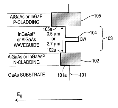
Figure 1 is a cross-sectional band-gap diagram of an apparatus according to a
first
embodiment of the present invention. An example of this embodiment can be a
semiconductor
diode laser that emits 0.98 ~m radiation so as to couple into an EDFA. The
apparatus includes a
substrate 101, an n-type cladding 102, a waveguide region 103 that includes
quantum wells 104
positioned at the center of the waveguide layer, and a p-type cladding 105. A
difference in the
bandgap energies 1 O 1 a exists between the n-type cladding and the substrate,
and a difference in
the bandgap energies 102a exists between the n-type cladding and the
waveguide. In the
embodiment represented by Figure 1, the difference in the bandgap energies
lOSa between the p-
type cladding and the waveguide is greater than the difference in the bandgap
energies 102a
CA 02398829 2002-07-19
WO 01/57974 PCT/USO1/01971
between the n-type cladding and the waveguide. Additionally, the energy
bandgap of layer 102 is
greater than energy bandgap of layer 103, but smaller than energy bandgap of
layer 105.
In this embodiment of the present invention, substrate 101 is a GaAs compound,
n-type
cladding 102 is an AIGaAs or InGaAsP compound, waveguide 103 is an InGaAsP or
AIGaAs
compound, and p-type cladding 105 is an AIGaAs or InGaP compound, quantum
wells 104
include InGaAs or InGaAsP compounds. The invention, however, is not limited to
these
compounds. Rather, the invention can use any compound that is practicable for
such devices.
Figure 2 is a refractive-index diagram of an apparatus according to an
embodiment of the
present invention. As can be seen in Figure 2, the difference in refractive
index between the p-
type cladding and the waveguide is greater than the difference in refractive
index between the n-
type cladding and the waveguide, thus forming an asymmetric optical
confinement for
propagation of a single-mode beam in the waveguide.
Figure 3 is a graphical representation of far-field divergence for the 0.98 ~m
embodiment
of the present invention, measured by the full width at half maximum (FWHM),
as a function of
waveguide width for a given set of materials. This figure can be used to
design a device with a
desired far-field divergence. For example, as can be seen in this figure, if a
far-field divergence
with a FWHM of 20 degrees is desired, one can make the waveguide either 0.5 ~m
or 2.7 ~m
wide.
Values of the waveguide thickness that provide 20 degrees vertical divergence
depend on
the compositions of the claddings and waveguide, but is approximately
proportional to the laser's
output wavelength. Levels of doping and vertical distribution of the dopants
in the cladding
should be optimized based upon two conditions. First, device resistance should
be minimized.
6
CA 02398829 2002-07-19
WO 01/57974 PCT/USO1/01971
Second, creating additional optical losses that are higher than other types of
internal losses
caused by scattering on the uniformities and absorption in the active region
should be avoided.
The second condition should be considered at least for a design with a modest
waveguide
thickness, because the optical field penetration into the cladding is very
small in the case of
asymmetric broad waveguide structures. In the asymmetric structures, the
optical field penetrates
only in the n-type cladding layers, and the n-doping should be limited by
additional optical
losses. For p-type cladding, a graded doping of 1-3 x 1018 cm 3 can be used.
One skilled in the art will appreciate that the thickness of the cladding
regions should be
large enough to prevent losses due to optical field penetration into the
substrate (or into the
contact layer (not shown in the figures)). For example, for the compounds
discussed above, a p-
type cladding with a thickness of 1 to 1.5 ~m is sufficient. For n-type
cladding, the thickness
should be different for embodiments that exhibit a broad waveguide (e.8., 2.7
~m ) than for
embodiments that exhibit a modestly-thick waveguide (e.8., 0.5 ~m ). For broad-
waveguide
embodiments, the n-type cladding thickness can be the same as the p-type
cladding thickness
(e.8., ~ 1 Vim). For a modestly-thick waveguide embodiment, a cladding
thickness of 3-4 ~m can
be used.
Figure 4 is a cross-sectional energy band-gap diagram of an apparatus
according to an
embodiment of the present invention. In this embodiment, the semiconductor
diode laser emits
1.48 ~m radiation. In this embodiment, substrate 401 is an InP compound, n-
type cladding 402
is an InGaAsP or InGaAIAs compound, waveguide 403 is an InGaAsP or InGaAIAs
compound,
and p-type cladding 405 is an InP or InAIAs compound. Quantum wells can be
InGaAsP or
InGaAs or InGaAIAs compounds. As is typically the case, waveguide 403 contains
a center-
7
CA 02398829 2002-07-19
WO 01/57974 PCT/USO1/01971
positioned quantum well or wells 404. As with the embodiment of Figure 1,
bandgap difference
402a, between n-type cladding 402 and waveguide 403, is smaller than bandgap
difference 405a,
between p-type cladding 405 and waveguide 403.
Figure 5 is a graph of refractive index as a function of vertical distance in
the laser
structure for the embodiment shown in Figure 4, but with two quantum wells. It
should be
appreciated that, in the present context, the term "vertical" is to be
understood in the context of
the figure, and is not an absolute direction. In other words, the refractive
index is shown in
Figure ~ as a function of distance, left to right, corresponding to the laser
structure shown in
Figure 4, bottom to top. As is characteristic of embodiments of the present
invention, the
difference in refractive index between p-type cladding 405 and waveguide 403
is larger than the
difference in refractive index between n-type cladding 402 and waveguide 403.
Vertical far-field beam divergence in the embodiment of Figures 4 and S is
again a
function of waveguide width, as is shown in Figure 6. As can be seen in this
figure, if a far-field
divergence with a FWHM of 20 degrees is desired, one can choose a waveguide
thickness of
either approximately 0.5 ~.m (modest waveguide thickness) or 3.5 p.m (broad
waveguide).
Figures 7 and 8 are graphs of the optical-confinement factor as a function of
waveguide
width. Figure 7 represents the optical-confinement factor for a 0.98 ~m laser,
and Figure 8
represents the optical-confinement factor for a 1.48 ~.m laser. The vertical
dashed lines in these
figures refer to the waveguide thickness providing approximately 20°-
22° vertical divergence.
This reduction of the optical confinement is beneficial for high-power
operation because the
power level at which catastrophic optical damage occurs is inversely
proportional to the optical
confinement factor. At a waveguide thickness of approximately 2.5 Vim, the
optical confinement
CA 02398829 2002-07-19
WO 01/57974 PCT/USO1/01971
factor is halved and the maximum output power is expected to be doubled.
Maximizing the asymmetry in the two refractive-index steps (i.e., between the
p-type
cladding and the waveguide, on the one hand, and between the n-type cladding
and the
waveguide, on the other hand) allows one to maximize the width of the
waveguide that can be
used without introducing additional transverse modes in generated laser
radiation. The
asymmetry in the two refractive-index steps depends on the asymmetry between
the two bandgap
differences (i.e., the bandgap difference between the p-type cladding and the
waveguide, on the
one hand, and between the n-type cladding and the waveguide, on the other
hand). Thus,
maximizing the refractive-index step on the p-type cladding side of the
waveguide, while
minimizing the refractive-index step on the n-type cladding side of the
waveguide, allows for the
widest waveguide without introducing non-zero even transverse modes.
The dependence of the maximum waveguide thickness WZ on the refractive indices
n2
and n3 is given by equation (1). Of course, this equation gives the
theoretical maximum, and in
practice the equal sign may not be exactly equal. At selected nz and n3, the
waveguide with a
centrally-positioned quantum well having the thickness W2 can provide laser
operation in the
transverse (vertical) zeroth-order mode, with maximally wide near-field
distribution and minimal
far-field divergence. The first and other even modes do not exist at W<_W2.
(Again, in practice,
this inequality becomes "less than or approximately equal to.") Additionally,
odd mode lasing is
eliminated by the centered positioning of the quantum wells in the waveguide.
(1)
9
CA 02398829 2002-07-19
WO 01/57974 PCT/USOI/01971
~,(2~c + Cos-lr~)
w= =
2~c (2n, (n, - n, ))°.s
where 7~ is the radiation wavelength, n~ is the refractive index of the
waveguide, n3 is the
refractive index of the n-cladding and the n2 is the refractive index of the p-
cladding and
I~n -n.)
:)
The desirable refractive index distribution can be achieved, in one embodiment
of the
present invention, when the following two criteria are met. First, the p-type
cladding layer must
be chosen such that the bandgap is maximized. Second, the n-type cladding
layer must be chosen
such that the n-type cladding has a bandgap that exceeds the waveguide's
bandgap by an amount
on the order of kT, where k is Boltzman's constant, and T is the temperature
of the device during
operation.
The present invention has been described in terms of several embodiments
solely for the
purpose of illustration. Persons skilled in the art will recognize from this
description that the
invention is not limited to the embodiments described, but may be practiced
with modifications
and alterations limited only by the spirit and scope of the appended claims.
In particular, the
present invention has been described in terms of particular embodiments (a
0.98 ~m laser and a
CA 02398829 2002-07-19
WO 01/57974 PCT/USO1/01971
1.48 ~.m laser) for ease of explanation and understanding. Any known
practicable materials and
their corresponding thicknesses, however, can be used, as long as the
functional relationship
described above between bandgap, index of refraction, and waveguide thickness
satisfies the
optical confinement and distribution/divergence criteria discussed above.
11