Note: Descriptions are shown in the official language in which they were submitted.
CA 02398837 2005-04-13
PROCESS FOR FABRICATING
ELECTROPHOTOGRAPHIC IMAGIN(J MEMBER
BACKGROUND OF THE INVENTION
1. Field of Invention
[0001] This invention relates in general to a process for fabricating
electrophotographic imaging members.
2. Description of Related Art
[0002] Typical electrophotographic imaging members comprise a
photoconductive layer comprising a single layer or composite layers. One type
of
composite photoconductive layer used in xerography is illustrated, for
example, in
U.S. Patent 4,265,990. The 990 patent describes a photosensitive member having
at
least two electrically operative layers. One layer comprises a photoconductive
layer
which is capable of photogenerating holes and injecting the photogenerated
holes into
a contiguous charge transport layer.
[0003] Generally, where the two electrically operative layers are supported
on a conductive layer, the photogenerating layer is sandwiched between the
contiguous charge transport layer and the supporting conductive layer. The
outer
surface of the charge transport layer is normally charged with a uniform
electrostatic
charge. The photosensitive member is then exposed to a pattern of activating
electromagnetic radiation, such as light. The activating electromagnetic
radiation
selectively dissipates the charge in illuminated areas of the photosensitive
member,
while leaving behind an electrostatic latent image in the non- illuminated
areas. This
electrostatic latent image may then be developed to form a visible image, by
depositing finely divided electrostatic toner particles on the surface of the
photosensitive member. The resulting visible toner image; can be transferred
to a
suitable receiving material, such as paper. This imaging process may be
repeated
many times with reusable photosensitive members.
[0004] As more advanced, complex, and highly sophisticated,
electrophotographic copiers, duplicators and printers have been developed,
greater
demands have been placed on the photoreceptor to meet stringent requirements
for the
production of high quality images. For example, to provide excellent toner
images
CA 02398837 2005-04-13
2
over many thousands of cycles, the numerous layers found in many modern
photoconductive imaging members must be uniform, free of defects, adhere well
to
adjacent layers, and exhibit predictable electrical characteristics within
narrow
operating limits. One type of multilayered photoreceptor that has been
employed, in
drum or belt form, in electrophotographic imaging systems comprises a
substrate, a
conductive layer, a charge blocking layer, an adhesive layer, a charge
generating layer,
and a charge transport layer. This photoreceptor may also comprise additional
layers,
such as an overcoating layer.
[0005] Excellent toner images may be obtained with this and other
multilayered photoreceptors. However, it has been found that the numerous
layers
limit the versatility of the multilayered photoreceptor. For example, when a
thick,
e.g., 29 micrometer, charge transport layer is formed in a single pass, a
"raindrop"
pattern forms on the exposed imaging surface of the final dried photoreceptor.
This is
discussed in detail in U.S. Patent 6,214,514 to Evans et al. This "raindrop"
phenomenon is a print defect caused by high frequency coating thickness
variations in
the relatively thick (e.g., 29 micrometer) charge transport layer. More
specifically, the
expression "raindrop", as employed herein, is defined as a high frequency
variation in
the layer thickness. The spatial period of this variation is in the 0.1 cm to
2.5 cm
range. The amplitude of this variation is between 0.5 micrometer and 1.5
micrometer.
The "raindrop" variation can also be defined on a per unit area basis. The
raindrop
defect can occur when the transport layer thickness variation is in the range
of 0.5 to
1.5 microns per sq. cm. The morphological structure of raindrop defect is
variable
and depends on where and how the device is coated. The structure can be
periodic or
random, symmetrical or oriented.
[0006] U.S. Patent No. 6,214,541 discloses a process for fabricating
electrophotographic imaging members including providing an imaging member
including a substrate coated with a charge generating layer having an exposed
surface,
applying a first solution including a charge transporting srnall molecule and
film-
forming binder to the exposed surface to form a first charl;e transporting
layer having
a thickness of greater than about 13 micrometers and less than about 20
micrometers
in the dried state and an exposed surface, and applying at least a second
solution
having a composition substantially identical to the first solution to the
exposed surface
CA 02398837 2005-04-13
3
of the first charge transportation layer to form at least a second continuous
charge
transporting layer, the at least second charge transporting layer having a
thickness in
the dried state of less than about 20 micrometers, the at least second charge
transporting layer, and any subsequent applied solution having a composition
S substantially identical to the first solution.
[0007] Although this is considered an acceptable solution, it results in an
extra coating pass leading to higher manufacturing costs.
SUMMARY OF THE INVENTYON
[0008] This invention provides systems and methods for fabricating an
electrophotographic imaging member having reduced raindrop variation.
[0009] This invention separately provides systems and methods for
achieving coating uniformity in a charge transport layer formed in a single
pass.
[0010] This invention separately provides systems and methods for reducing
raindrop defects in charge transport layers formed in a single pass.
[0011] The systems and methods for fabricating electrophotographic
imaging members according to this invention comprise forming an imaging member
having a substrate coated with a charge transport layer, where the material
used to
form the charge transport layer has a viscosity of about 1500-2100 cps.
[0012] If desired, after forming the charge transport layer, the resulting
electrophotographic imaging member may optionally be coated with any suitable
known or later-developed overcoating layer.
[0013] Other layers, such as conventional ground strips comprising, for
example, conductive particles dispersed in a film-forming binder, may be
applied to
one edge of the multilayer photoreceptor and in contact with the conductive
surface,
blocking layer, adhesive layer or charge generating layer.
[0014] In various exemplary embodiments, a back coating layer may be
applied to the side of the substrate opposite the multilayer photoreceptor to
provide
flatness and/or abrasion resistance. This back coating layer may comprise an
organic
polymer or inorganic polymer that is electrically insulatin;; or slightly semi-
conductive.
[0015] The multilayer photoreceptor manufactured according to this
invention may be employed in any suitable conventional or later-developed
CA 02398837 2005-04-13
4
electrophotographic imaging process which utilizes charging prior to imagewise
exposure to activating electromagnetic radiation. Conventional positive or
reversal
development techniques may be employed to form a marking material image on the
imaging surface of the electrophotographic imaging member of this invention.
[0015.1] According to an aspect of the present invention, there is
provided a method of producing an electrophotograhic imaging member
comprising:
extrusion coating a substrate comprising an electrically conductive surface
layer and a charge generating layer by applying a charge transport layer
adjacent the
charge generating layer in a single coating having a viscosity of about 1500-
2100 cps.
[0015.2] According to another aspect of the present invention, there is
provided a method of producing an electrophotograhic imaging member consisting
of
extrusion coating a substrate comprising an electrically conductive surface
layer and a charge generating layer by applying a charge transport layer
adjacent the
charge generating layer in a single coating having a viscosity of about 1500-
2100 cps,
wherein the extrusion coating is selected from the group consisting of
extrusion single
slot coating; extrusion single layer slide coating and extrusion single layer
curtain
coating.
[0016] These and other features and advantages of this invention are
described in, or are apparent from, the following detailed description of
various
exemplary embodiments of the systems and methods according to this invention.
BRIEF DESCRIPTION OF THE DRAWINGS
[0017] Various exemplary embodiments of this invention will be described
in detail, with reference to the following figures, wherein:
[0018] Fig. 1 illustrates a schematic cross-sectional view of a single slot
coating system according to this invention;
[0019] Fig. 2 illustrates a schematic cross-sectional view of a single layer
slide coating system according to this invention;
[0020] Fig. 3 illustrates a schematic cross-sectional view of a single layer
curtain coating system according to this invention;
[0021] Fig. 4 illustrates a monochromatic interference image of high
frequency thickness variability of a charge transport layer of a control
photoreceptor
exhibiting the raindrop defect; and
CA 02398837 2005-04-13
4a
[0022] Fig. 5 illustrates a monochromatic interference image of high
frequency thickness variability of a first charge transport layer of a
photoreceptor
resulting from the systems and methods according to this invention.
DETAILED DESCRIPTION OF EXEMPLAR.' EMBODIMENTS
[0023] Generally, most types of photoreceptors comprise a supporting
substrate having an electrically conductive surface layer, an optional charge
blocking
layer on the electrically conductive surface, an optional adhesive layer, a
charge
CA 02398837 2002-08-20
generating layer on the blocking layer and a transport layer on the charge
generating
layer.
[0024] The supporting substrate may be opaque or substantially transparent
and may be fabricated from various materials having the requisite mechanical
properties. The supporting substrate may comprise electrically non-conductive
or
conductive, inorganic or organic composition materials. The supporting
substrate
may be rigid or flexible and may have a number of different configurations
such as,
for example, a cylinder, sheet, a scroll, an endless flexible belt, or the
like. In various
exemplary embodiments, the supporting substrate is in the form of an endless
flexible
belt, and comprises a commercially available biaxially-oriented polyester,
such as
Mylar~ and available from E.I, du Pont de Nemours & Co., or Melinex~ available
from ICI. Other exemplary electrically non-conducing materials known for this
purpose include polyesters, polycarbonates, polyamides, polyurethanes, and the
like.
[0025] The average thickness of the supporting substrate depends on
numerous factors, including economic considerations. A flexible belt may be of
substantial thickness, for example, over 200 micrometers, or have a minimum
thickness less than SO micrometers, provided there are no adverse affects on
the final
multilayer photoreceptor device. In various embodiments of a flexible belt
supporting
substrate, the average thickness of the support layer ranges from about 65
micrometers
to about 150 micrometers. The average thickness of the support layer ranges
from
about 75 micrometers to about 125 micrometers for improved flexibility and
reduced
stretch when cycled around small diameter rollers, such as, for example, 12
millimeter
diameter rollers.
[0026] The electrically conductive surface layer may vary in average
thickness over substantially wide ranges depending on the optical transparency
and
flexibility desired for the multilayer photoreceptor. Accordingly, when a
flexible
multilayer photoreceptor is desired, the thickness of the electrically
conductive surface
layer may be between about 20 Angstroms to about 750 Angstroms. The thickness
of
the electrically conductive surface layer may range from about 50 Angstroms to
about
200 Angstroms for a particularly useful combination of electrical
conductivity,
flexibility and light transmission.
CA 02398837 2002-08-20
6
[0027] The electrically conductive surface layer may be a metal layer
formed, for example, on the support layer by a coating technique, such as a
vacuum
deposition. Typical metals employed for this purpose include aluminum,
zirconium,
niobium, tantalum, vanadium and hafnium, titanium, nickel, stainless steel,
chromium, tungsten, molybdenum, and the like. Useful metal alloys may contain
two
or more metals, such as zirconium, niobium, tantalum, vanadium and hafnium,
titanium, nickel, stainless steel, chromium, tungsten, molybdenum, and the
like.
[0028] Regardless of the technique employed to form the metal layer, a thin
layer of metal oxide may form on the outer surface of most metals upon
exposure to
air. Thus, when other layers overlying a (metal) electrically conductive
surface layer
are described as "contiguous" layers, it is intended that these overlying
contiguous
layers may, in fact, contact a thin metal oxide layer that has formed on the
outer
surface of the oxidizable metal layer. For improved electrical behavior, the
average
thickness for the thin metal oxide layers should be between about 30 Angstroms
and
1 S about 60 Angstroms.
[0029] Generally, for rear erase exposure, a conductive layer light
transparency of at least about 1 S percent is desirable. The light
transparency allows
the design of machines employing erase from the rear. The electrically
conductive
surface Layer need not be limited to metals. Other examples of conductive
layers may
be combinations of materials such as conductive indium-tin oxide as a
transparent
layer for light having a wavelength between about 4000 Angstroms and about
7000
Angstroms or a conductive carbon black dispersed in a plastic binder as an
opaque
conductive layer.
[0030] After depositing the electrically conductive surface layer, an optional
blocking layer may be applied to the electrically conductive surface layer.
Generally,
electron blocking layers for positively charged photoreceptors allow holes
from the
imaging surface of the photoreceptor to migrate toward the conductive layer.
For use
in negatively charged systems, any suitable blocking layer capable of forming
an
electronic barrier to holes between the adjacent multilayer photoreceptor
layers and
the underlying conductive layer may be used. The blocking layer may be organic
or
inorganic and may be deposited by any suitable technique. For example, if the
CA 02398837 2005-04-13
7
blocking layer is soluble in a solvent, it may be applied as a solution. The
solvent can
subsequently be removed from the solution by any conventional method, such as
by
drying.
[0031] Typical blocking layers include polyvinylbutyral, organosilanes,
epoxy resins, polyesters, polyamides, polyurethanes, pyroxyline vinylidene
chloride
resin, silicone resins, fluorocarbon resins and the like containing an organo-
metallic
salt. The blocking layer may comprise a reaction product between a hydrolyzed
silane
and a thin metal oxide layer formed on the outer surface of an oxidizable
metal
electrically conductive surface. Other blocking layer materials include
nitrogen-
containing siloxanes or nitrogen- containing titanium compounds such as
trimethoxysilyl propylene diamine, hydrolyzed trimethox;ysilylpropylethylene
diamine, N- beta-(aminoethyl)-gamma-aminopropyltrimethoxy silane, isopropyl- 4-
aminobenzene sulfonyl, di(dodecylbenzene sulfonyl) titanate, isopropyl-di(4-
aminobenzoyl)isostearoyl titanate, isopropyl- tri(N-ethylamino-ethylamino)
titanate,
isopropyl trianthranil titanate, isopropyl-tri-(N,N-dimethylethylamino)
titanate,
titanium-4-amino benzene sulfonatoxyacetate, titanium 4-~ aminobenzoate-
isostearate-
oxyacetate, [H2N(CH2)4]CH3Si(OCH3)2, (gamma-aminobutyl)methyl
diethoxysilane, and [H2N(CH2)3]CH3Si(OCH3)2 (gamma-
aminopropyl)methyldiethoxy silane, as disclosed in U.S. Patents 4,291,110,
4,338,387
and 4,286,033.
(0032] In various exemplary embodiments, the blocking layer is continuous
and usually has an average thickness of less than about 5000 Angstroms. In
various
exemplary embodiments, the blocking layer has a thickness between about 50
Angstroms and about 3000 Angstroms. This thickness range tends to facilitate
charge
neutralization after light exposure of the multilayer photoreceptor and
improve
electrical performance. The blocking layer may be applied by any suitable
known or
later-developed technique, such as spraying, dip coating, draw bar coating,
gravure
coating, silk screening, air knife coating, reverse roll coating, vacuum
deposition,
extrusion coating, slot coating, chemical treatment and the like. In various
exemplary
embodiments, for convenience in obtaining thin layers, the blocking layers are
applied
CA 02398837 2005-04-13
g
in the form of a dilute solution. In this case, the solvent is removed after
depositing of
the coating by any suitable known or later-developed technique, such as
vacuum,
heating and the like. Generally, a weight ratio of blocking layer material and
solvent
of between about 0.05:100 and about 0.5:100 is satisfactory for spray coating.
A
typical siloxane coating is described in U.S. Patent 4,464,450.
[0033] If desired, an optional adhesive layer may be applied over the hole
blocking layer or over the conductive surface. Typical adhesive layers include
a
polyester resin, such as Vitel PE-100°, Vitel PE-200", Vitel PE-
200D°, and Vitel PE-
222°, all available from Goodyear Tire and Rubber Co., I)uPont 49,000
polyester,
polyvinyl butyral, and the like. When an adhesive layer is employed, the
adhesive
layer is, in various exemplary embodiments, continuous. In various exemplary
embodiments, the adhesive layer has an average dry thickness between about 200
Angstroms to about 900 Angstroms. The adhesive dry layer may have an average
dry
thickness between about 400 Angstroms to about 700 Angstroms.
[0034] Any suitable known or later-developed solvent or solvent mixtures
may be employed to form a coating solution for the adhesive layer material.
Typical
solvents include tetrahydrofuran, toluene, methylene chloride, cyclohexanone,
and
mixtures of these materials. In various exemplary embodiments to achieve a
continuous adhesive layer dry thickness of about 900 Angstroms or less using
gravure
coating, the solids concentration of the solution is about 2 percent to about
5 percent
by weight based on the total weight of the coating mixture of resin and
solvent.
However, any suitable known or later-developed technique may be utilized to
mix and
apply the adhesive layer coating mixture to the charge blocking layer. Typical
application techniques include spraying, dip coating, roll coating, wire wound
rod
coating, extrusion or slot coating, and the like. Drying the deposited coating
may be
effected by any suitable known or later-developed technique, such as oven
drying,
infra red radiation drying, air drying and the like.
[0035] A charge generating layer is applied over the blocking layer, or over
the adhesive layer, if either is employed. The charge generating layer can
then be
overcoated with a charge transport layer, as described herein. Examples of a
charge
CA 02398837 2002-08-20
9
generating layer include inorganic photoconductive particles, such as
amorphous
selenium, trigonal selenium, and selenium alloys, such as selenium-tellurium,
selenium-tellurium-arsenic, selenium arsenide and mixtures of these alloys,
and
organic photoconductive particles, including various phthalocyanine pigments,
such
as the X-form of metal-free phthalocyanine, which is described in
U.S. Patent 3,357,989, metal phthalocyanines, such as vanadyl phthalocyanine,
titanyl
phthalocyanines, hydroxycalcium phthalocyanines and copper phthalocyanine. Any
suitable or later developed pigment such as quinacridones (available from
DuPont
under the trade name Monastral Red°, Monastral Violet° and
Monastral Red Y°), may
be used. Other pigments include Vat Orange 1° and Vat Orange 3°,
trade names for
dibromoanthrone pigments, benzimidazole perylene, substituted 3,4-
diaminotriazines
as disclosed in U.S. Patent 3,442,781. Polynuclear aromatic quinones available
from
Allied Chemical Corporation under the tradename Indofast Double
Scarlet°, and
Indofast Violet Lake B°. Indofast Brilliant Scarlet° and
Indofast Orange°. The
pigments are dispersed in a film-forming polymeric binder.
[0036] Selenium, selenium alloy, benzimidazole perylene, and the like and
mixtures of these materials may be formed as a continuous, homogeneous charge
generating layer. Benzimidazole perylene compositions are well known and
described, for example, in U.S. Patent 4,587,189. Multiphotogenerating layer
compositions may be utilized, where an additional photoconductive layer may
enhance or reduce the properties of the charge generating layer. Examples of
this type
of configuration are described in U.S. Patent 4,415,639. Other suitable charge
generating materials known in the art may also be utilized, if desired. Charge
generating binder layers comprising particles or layers including a
photoconductive
material, such as vanadyl phthalocyanine, titanyl phthalocyanines, metal-free
phthalocyanine, benzimidazole perylene, amorphous selenium, trigonal selenium,
selenium alloys such as selenium-tellurium, selenium-tellurium-arsenic,
selenium
arsenide and the like, and mixtures of these selenium alloys are particularly
useful
because of their sensitivity to white light. Vanadyl phthalocyanine, titanyl
phthalocyanines, metal-free phthalocyanine, hydroxygallium phthalocyanine and
CA 02398837 2002-08-20
tellurium alloys are also particularly useful because these materials provide
the
additional benefit of being sensitive to infra-red light.
[0037] Numerous inactive resin materials may be employed in the charge
generating binder layer including those described, for example, in
5 U.S. Patent 3,121,006. Typical organic resinous binders include
thermoplastic and
thermosetting resins, such as polycarbonates, polyesters, polyamides,
polyurethanes,
polystyrenes, polyarylethers, polyarylsulfones, polybutadienes, polysulfones,
polyethersulfones, polyethylenes, polypropylenes, polyimides,
polymethylpentenes,
polyphenylene sulfides, polyvinyl acetate, polysiloxanes, polyacrylates,
polyvinyl
10 acetals, polyamides, polyimides, amino resins, phenylene oxide resins,
terephthalic
acid resins, epoxy resins, phenolic resins, polystyrene and acrylonitrile
copolymers,
polyvinylchloride, vinylchloride and vinyl acetate copolymers, acrylate
copolymers,
alkyd resins, cellulosic film formers, poly(amide-imide), styrene-butadiene
copolymers, poly styrene-vinylpyridine copolymers, vinylidenechloride-
vinylchloride
copolymers, vinylacetate-vinylidenechloride copolymers, styrene- alkyd resins,
and
the like. These polymers may be block, random or alternating copolymers.
[0038] An active transporting polymer containing charge transporting
segments may also be employed as the binder in the charge generating layer.
These
polymers are particularly useful when the concentration of carrier-generating
pigment
particles is low and the average thickness of the earner-generating layer is
substantially thicker than about 0.7 micrometer. One active polymer commonly
used
as a binder is polyvinylcarbazole, which is able to transport carriers which
would
otherwise be trapped in the charge transport layer.
[0039] Electrically active polymeric arylamine compounds can be employed
in the charge generating layer to replace the polyvinylcarbazole binder or
another
active or inactive binder. Part or all of the active resin materials to be
employed in the
charge generating layer may be replaced by electrically active polymeric
arylamine
compounds.
[0040] The photogenerating composition or pigment is present in the
resinous binder composition in various amounts. Generally, however, the
photogenerating composition or pigment forms from about 5 percent by volume to
CA 02398837 2002-08-20
11
about 90 percent by volume of the photogenerating pigment, which is dispersed
in
about 95 percent by volume to about 10 percent by volume of the resinous
binder,
respectively. In various exemplary embodiments, the photogenerating pigment
forms
from about 20 percent by volume to about 30 percent by volume, which is
dispersed
in about 80 percent by volume to about 70 percent by volume of the resinous
binder
composition, respectively. In various exemplary embodiments, about 8 percent
by
volume of the photogenerating pigment is dispersed in about 92 percent by
volume of
the resinous binder composition.
[0041 ] For those exemplary embodiments in which the charge generating
layers do not contain a resinous binder, the charge generating layer may
comprise any
suitable, known or later-developed homogeneous photogenerating material.
Typical
homogenous photogenerating materials include inorganic photoconductive
compounds, such as amorphous selenium, selenium alloys, such as selenium-
tellurium, selenium- tellurium-arsenic, and selenium arsenide, and organic
materials,
such as benzamidazole perylene, vanadyl phthalocyanine, chlorindium
phthalocyanine, chloraluminum phthalocyanine, and the like.
[0042] The charge generating layer, containing photoconductive
compositions and/or pigments and the resinous binder material, generally
ranges in
average thickness from about 0.1 micrometer to about 5 micrometers. A charge
generating layer having an average thickness from about 0.3 micrometer to
about 3
micrometers is particularly useful. The charge generating layer thickness is
related to
binder content. Higher binder content compositions generally result in thicker
layers
for photogeneration. Thicknesses outside these ranges can be used provided the
results to be obtained by this invention are achieved.
[0043] The active charge transport layer may comprise any suitable known
or later-developed non-polymeric small molecule charge transport material
capable of
supporting the injection of photogenerated holes and electrons from the charge
generating layer and allowing the transport of these holes or electrons
through the
charge transport layer to selectively discharge the surface charge. The active
charge
transport layer not only transports holes or electrons, but also protects the
charge
CA 02398837 2002-08-20
12
generating layer from abrasion or chemical attack. Therefore, the active
charge
transport layer also extends the operating life of the photoreceptor imaging
member.
[0044] In various exemplary embodiments, the active charge transport layer
is a substantially non-photoconductive material which supports the injection
of
photogenerated holes or electrons from the charge generating layer. In various
exemplary embodiments, the active charge transport layer is transparent when
the
charge generating layer is exposed through the active charge transport layer.
This
ensures that most of the incident radiation is utilized by the underlying
charge
generating layer to efficiently photogenerate charge. The active charge
transport
layer, in conjunction with the charge generating layer, act as an insulator to
the extent
that an electrostatic charge placed on the active charge transport layer is
not conducted
in the absence of activating illumination. For reasons of convenience, the
discussion
will refer to charge carriers or hole transport. However, transporting
electrons is also
contemplated as within the scope of this invention.
[0045] Any suitable known or later-developed soluble non-polymeric small
molecule transport material may be employed in the charge transport layer
coating
mixture. This small molecule transport material is dispersed in an
electrically inactive
polymeric film, forming materials to make these materials electrically active.
These
non-polymeric activating materials are added to those film-forming polymeric
materials which are incapable of supporting the injection of photogenerated
holes
from the generation material and incapable of allowing the transport of these
holes
through the active change transport layer. This will convert the electrically
inactive
polymeric material to a material capable of supporting the injection of
photogenerated
holes from the charge generating material and capable of allowing the
transport of
these holes through the active charge transport layer to discharge the surface
charge
on the active layer.
[0046] Any suitable known or later-developed non-polymeric small
molecule charge transport material which is soluble or dispersible on a
molecular
scale in a film-forming binder and able to achieve the proper viscosity may be
utilized
in the continuous phase of the active charge transport layer according to this
invention. The charge transport molecule should be capable of transporting
charge
CA 02398837 2002-08-20
13
carriers injected by the charge injection enabling particles in an applied
electric field.
The charge transport molecules may be hole transport molecules or electron
transport
molecules. Typical charge transporting materials include the following:
[0047] Diamine transport molecules are described in U.S. Patents 4,306,008,
4,304,829, 4,233,384, 4,115,116, 4,299,897, 4,265,990 and 4,081,274. Typical
diamine transport molecules include N,N'-Biphenyl-N,N'-bis(alkylphenyl)-[1,1'-
biphenyl]-4,4'-diamine, where the alkyl is, for example, methyl, ethyl,
propyl, n-butyl,
etc., such as N,N'-Biphenyl-N,N'-bis(3"-methylphenyl)-[1,1'-biphenyl]-4,4'-
diamine,
N,N'-Biphenyl-N,N'-bis(4-methylphenyl)-[1,1'-biphenyl]-4,4'-diamine, N,N'-
diphenyl-
N,N'-bis(2-methylphenyl)-[1,1'-biphenyl]-4,4'-diamine, N,N'-Biphenyl-N,N'-
bis(3-
ethylphenyl)-[ 1,1'-biphenyl]-4,4'-diamine, N,N'-Biphenyl-N,N'-bis(4-
ethylphenyl)-
[ 1,1'-biphenyl]-4,4'-diamine, N,N'-Biphenyl-N,N'-bis(4-n-butylphenyl)-[ 1,1'-
biphenyl]-4,4'-diamine, N,N'-Biphenyl-N,N'-bis(3-chlorophenyl)-[ 1,1'-
biphenyl]-4,4'-
diamine, N,N'-Biphenyl-N,N'-bis(4-chlorophenyl)-[ l, l'-biphenyl]-4,4'-
diamine, N,N'-
Biphenyl-N,N'-bis(phenylmethyl)-[1,1'-biphenyl]-4,4'-diamine, N,N,N',N'-
tetraphenyl-
[2,2'-dimethyl-1,1'-biphenyl]-4,4'-diamine, N,N,N',N'-tetra(4-methylphenyl)-
[2,2'-
dimethyl-1,1'-biphenyl]-4,4'-diamine, N,N'-Biphenyl-N,N'-bis(4-methylphenyl)-[
2,2'-
dimethyl-1,1'-biphenyl]-4,4'-diamine, N,N'-Biphenyl-N,N'-bis(2-methylphenyl)-
[2,2'-
dimethyl-1,1'-biphenyl]-4,4'-diamine, N,N'-Biphenyl-N,N'-bis(3-methylphenyl)-
[2,2'-
dimethyl-1,1'-biphenyl]-4,4'-diamine, N,N'-Biphenyl-N,N'-bis(3-methylphenyl)-
pyrenyl-1,6-diamine, and the like.
[0048] Pyrazoline transport molecules are disclosed in
U.S. Patents 4,315,982, 4,278,746, and 3,837,851. Typical pyrazoline transport
molecules include 1-[lepidyl-(2)]-3-(p-diethylaminophenyl)-S-(p-
diethylaminophenyl)pyrazoline, 1-[quinolyl-(2)]-3-(p-diethylaminophenyl)-5-(p-
diethylaminophenyl)pyrazoline, 1-[pyridyl-(2)]-3-(p-diethylaminostyryl)-5-(p-
diethylaminophenyl)pyrazoline, 1-[6-methoxypyridyl-(2)]-3-(p-
diethylaminostyryl)-5-
(p-diethylaminophenyl)pyrazoline, 1-phenyl-3-[p-dimethylaminostyryl]-5-(p-
dimethylaminostyryl)pyrazoline, 1-phenyl-3-[p-diethylaminostyryl]-5-(p-
diethylaminostyryl)pyrazoline, and the like.
CA 02398837 2002-08-20
14
[0049] Substituted fluorene charge transport molecules are described in
U.S. Patent 4,245,021. Typical fluorene charge transport molecules include 9-
(4'-
dimethylaminobenzylidene)fluorene, 9-(4'-methoxybenzylidene)fluorene, 9-(2',4'-
dimethoxybenzylidene)fluorene, 2-nitro-9-benzylidene-fluorene, 2-nitro-9-(4'-
diethylaminobenzylidene)fluorene and the like.
[0050] Oxadiazole transport molecules such as 2,5-bis(4-
diethylaminophenyl)-1,3,4-oxadiazole, pyrazoline, imidazole, triazole, and
others are
described in German Patents 1,058,836, 1,060,260 and 1,120,875 and
U.S. Patent 3,895,944.
[0051] Hydrazone including, for example, p-diethylaminobenzaldehyde-
(diphenylhydrazone), o-ethoxy-p-diethylaminobenzaldehyde-(diphenylhydrazone),
o-
methyl-p-diethylaminobenzaldehyde-(diphenylhydrazone), o-methyl-p-
dimethylaminobenzaldehyde-(diphenylhydrazone), p-dipropylaminobenzaldehyde-
(diphenylhydrazone), p-diethylaminobenzaldehyde-(benzylphenylhydrazone), p-
dibutylaminobenzaldehyde- (diphenylhydrazone), p-dimethylaminobenzaldehyde-
(diphenylhydrazone) and the like described, for example in US-A 4,150,987.
Other
hydrazone transport molecules include compounds such as 1-
naphthalenecarbaldehyde 1-methyl-1-phenylhydrazone, 1-
naphthalenecarbaldehyde l,l-phenylhydrazone, 4-methoxynaphthlene-1-
carbaldehyde 1-methyl-1-phenylhydrazone and other hydrazone transport
molecules
are described, for example in U.S. Patents 4,385,106, 4,338,388, 4,387,147,
4,399,208, and 4,399,207.
[0052] Still another charge transport molecule is carbazole phenyl
hydrazone. Typical examples of carbazole phenyl hydrazone transport molecules
include 9-methylcarbazole-3-carbaldehyde-1,1-diphenylhydrazone, 9-
ethylcarbazole-
3-carbaldehyde-1-methyl-1-phenylhydrazone, 9-ethylcarbazole-3-carbaldehyde-1-
ethyl-1-phenylhydrazone, 9-ethylcarbazole-3-carbaldehyde-1-ethyl-1-benzyl-1-
phenylhydrazone, 9-ethylcarbazole-3-carbaldehyde-1,1-diphenylhydrazone, and
other
suitable carbazole phenyl hydrazone transport molecules described, for
example, in
U.S. Patent 4,256,821. Similar hydrazone transport molecules are described,
for
example, U.S. Patent 4,297,426.
CA 02398837 2002-08-20
[0053] Tri-substituted urethanes such as alkyl-bis(N,N-dialkylaminoaryl)
methane, cycloalkyl-bis(N,N-dialkylaminoaryl)methane, and cycloalkenyl-bis(N,N-
dialkylaminoaryl)methane are described, for example, in U.S. Patent 3,820,989.
[0054] In various exemplary embodiments, the charge transport layer
5 forming solution comprises an aromatic amine compound as the activating
compound.
One particularly useful charge transport layer composition that can be used in
the
charge transport layer coating fabrication method according to this invention
comprises from about 35 percent to about 50 percent by weight of at least one
charge
transporting aromatic amine compound, and about 65 percent to about 55 percent
by
10 weight of a polymeric film-forming resin in which the aromatic amine is
soluble. The
substituents should be free from electron withdrawing groups, such as N0~
groups, CN
groups, and the like. Typical aromatic amine compounds include, for example,
triphenylmethane, bis(4-diethylamine-2-methylphenyl)phenylmethane; 4'-4"-
bis(diethylamino)-2',2"-dimethyltriphenylmethane, N,N'-bis(alkylphenyl)-[1,1'-
15 biphenyl]-4,4'-diamine wherein the alkyl is, for example, methyl, ethyl,
propyl, n-
butyl, etc., N,N'-diphenyl-N,N'-bis(chlorophenyl)-[ 1,1'-biphenyl]-4,4'-
diamine, 1,1'-
biphenyl)-4,4'-diamine, and the like dispersed in an inactive resin binder.
[0055] Any suitable known or later-developed soluble inactive film-forming
binder may be utilized in the charge transport layer coating mixture. The
inactive
polymeric film-forming binder may be soluble, for example, in methylene
chloride,
chlorobenzene or other suitable solvent. Typical inactive polymeric film-
forming
binders include polycarbonate resin, polyester, polyarylate, polyacrylate,
polyether,
polysulfone, and the like. Molecular weights can vary, for example, from about
20,000 to about 1,500,000. Polycarbonates are particularly useful as film-
forming
polymers for charge transport layers. Typical film-forming polymer
polycarbonates
include, for example, bisphenol polycarbonate, poly(4,4'-isopropylidene
diphenyl
carbonate), 4,4'-cyclohexylidene diphenyl polycarbonate, bisphenol A type
polycarbonate of 4,4'-isopropylidene (commercially available form Bayer AG as
Makrolon~), poly(4,4'-diphenyl-1,1'-cyclohexane carbonate) and the like. The
polycarbonate resins typically employed for charge transport layer
applications have a
weight-average molecular weight from about 70,000 to about 150,000.
CA 02398837 2005-04-13
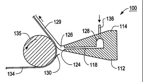
16
[0056] Fig. 1 illustrates a single slot coating applicator assembly 100. Slot
coating dies are well lcnown and are described, for example, in United States
Patents 4,521,457 and 5,614,260. The single slot coating applicator assembly
100
comprises a lower lip 112 and an upper lip 114 that combine to form passageway
118.
The passageway 118 is, in various exemplary embodiments, flat and/or narrow.
The
passageway 118 leads from a manifold 128 to a single exit slot 124.
[0057] A small molecule transport layer coating; dispersion having a
viscosity of between approximately 1500-2100 cps is fed into the manifold 128
through a feed pipe 136 and is extruded as a ribbon-like stream 126 through
the
passageway 118 and out of the single exit slot 124 onto substrate 134 as a
charge
transport layer 129. The substrate 134 is supported by a rotatable roll 135.
As shown
in Fig. 1, the ribbon-like stream 126 of coating material forming the charge
transport
layer is deposited across a gap 130 on the substrate 134 in a very thin layer
having a
thickness of approximately 29 microns. The width, thickness, and the like of
the
ribbon-like stream 126 can be varied in accordance with factors such as the
viscosity
of the coating composition, the desired thickness for the coating layer, and
the width
of the substrate 134 on which the coating compositions are applied, and the
like.
[0058] End dams (not shown) are secured to the ends of the lower lip 112
and the upper lip 114 of the single slot coating applicator assembly 110 to
confine the
coating composition within the manifold 128 and the passageway 118 as the
coating
composition travels from the feed pipe 136 through the manifold 128, to the
exit
slot 124. The length of the passageway 118 should be sufficiently long to
ensure
laminar flow. Controlling the distance of the exit slot 124 from the substrate
134
enables the ribbon-like stream 126 of the coating composition to bridge the
gap 130
between the exit slot 124 and the substrate 134, depending upon the viscosity
of the
coating composition, the rate of flow of the coating composition through the
passageway 118, and the relative rate movement between the single slot coating
applicator assembly 100 and the substrate 134.
[0059] As conventional in the art, the coating composition is supplied from
reservoirs (not shown) using a conventional pump or other suitable known or
later-
CA 02398837 2005-04-13
17
developed devices or apparatus, such as a gas pressure system (not shown). The
surfaces of the passageway 118 are precision ground to ensure accurate control
of the
thickness and uniformity of the ribbon-like stream 126 on the substrate 134.
The
coated substrate 134 is thereafter transported to any suitable drying device
to dry the
charge generating layer coating and charge transport layer coating.
[0060] Fig. 2 illustrates a slide die assembly 150 positioned adjacent to the
substrate 134. The slide die assembly 150 comprises an inclined land 152
adjacent to
and downstream from a passageway 154. The angle of slope of the inclined land
152
is dependent on the viscosity of the coating composition. In general, steeper
angles of
slope should be employed for higher viscosity coating compositions. A charge
transport layer coating solution having a viscosity of between 1500-2100 cps
is fed
into the manifold 128 through the feed pipe 136 and is extruded as ribbon-like
stream 158 through the passageway 154 and out onto the land 152, where the
stream 158 flows by gravity toward the substrate 134. As in Fig. l, the
substrate 134
is supported by a rotatable roll 135.
[0061] The charge transport layer coating material forming the ribbon-like
stream 158 flows by gravity over the land 152 and is deposited on the
substrate 134 as
a charge transport layer 159. A lip 156, located at the lower end of the land
152, is
positioned close to, but spaced from, the surface of the substrate 134 by a
gap 130 to
prevent the ribbon-like stream 158 of coating material from escaping
downwardly
through the narrow gap 130 between the substrate 134 and the slide die
assembly 150.
As with single slot coating applicator assembly described above, end dams (not
shown) are used to confine the coating compositions within the manifold 128
and the
passageway 154 as the coating composition travels from the feed pipe 130,
through
the manifold 128, to the inclined land 152. The coated substrate 134 is
thereafter
transported to any suitable known or later developed dryir,~g device to dry
coating
material forming the charge generating layer and the ribbon-like stream 158 of
material used to form charge transport layer coating.
[0062] Fig. 3 illustrates a curtain die assembly 140, which, although similar
in construction to the slide die assembly 150 illustrated in Fig. 2, is
positioned further
away from the substrate 134 to facilitate a falling curtain 147 of the charge
transport
CA 02398837 2005-04-13
18
layer coating stream 146 prior to it being deposited on the; exposed surface
of the
substrate 134. The curtain die assembly 140 comprises am inclined land 142
adjacent
to and downstream from a passageway 144. Depending on the coating solution
behavior, the inclined land 142 is aligned to generate maximum flow
uniformity. The
angle of slope for the inclined land 142 is dependent on the viscosity of the
coating
composition used to form the charge transport coating stream 146. In general,
steeper
angles of slope should be employed for higher viscosity coating compositions.
[0063] A charge transport layer coating solution having a viscosity of
between 1500-2100 cps is fed into the manifold 128 through the feed pipe 136
and is
extruded as a ribbon-like stream 146 through the passageway 144 and out onto
the
inclined land 142, where the ribbon-like stream 146 flows by gravity toward
the
substrate 134. The substrate 134 is supported by the rotatable roll 135. In
various
exemplary embodiments, the exposed upper surface of the substrate 134 is
aligned in
a substantially horizontal attitude relative to the ribbon-lil;e stream 146 at
the location
where the falling curtain 147 of the charge transport layer coating 149 are
deposited
on the substrate 134. Thus, the ribbon-like stream 146 of charge transport
layer
coating material flows by gravity over the inclined land 142, forms a falling
curtain
147, and deposits on the substrate 134 as the charge transport layer 149. A
lip 156,
located at the lower end of the inclined land 142, directs tile falling
curtain 147 away
from the curtain die assembly 100. As with the slide coating applicator
assembly 150
described above, end dams (not shown) are used to confine the coating
compositions
within the manifold 128 and the passageway 144 as the coating composition
travels
from the feed pipe 136, through the manifold 128, to the inclined land 142.
The
coated substrate 134 is thereafter transported to any suitable drying device
to dry the
charge transport layer coating.
[0064] Selecting the die passageway height determines the thickness of the
ribbon 146 of the coating material as it traverses through the passageway 144.
The
slope of an inclined land and the like generally depends upon factors such as
the fluid
viscosity, the surface tension, the flow rate, the distance to~ the surface of
the support
member 134, the relative movement between the curtain die and assembly 140 and
the
substrate 134, the desired thickness of the charge transport layer, and the
like.
CA 02398837 2002-08-20
19
Regardless of the technique employed, the flow rate and distance should be
regulated
to avoid splashing, dripping and puddling of the coating materials. For the
type of die
described in Fig. 1, generally satisfactory results may be achieved with
narrow
passageway heights between about 200 micrometers and about 1500 micrometers in
the passageways for charge transport layers. The roof, sides and floor of the
narrow
die passageways should preferably be parallel and smooth to ensure achievement
of
laminar flow. The length of the narrow extrusion slot from the manifold to the
outlet
opening should be sufficient to ensure achievement of laminar flow and uniform
coating solution distribution.
[0065] Relative speeds between an extrusion coating die assembly and the
surface of the substrate 134 up to about 200 feet per minute have been tested.
However, it is believed that greater relative speeds may be utilized if
desired. The
relative speed should be controlled in accordance with the flow velocity of
the ribbon-
like streams 126, 146 and/or 156 of the coating material used to form the
charge
transport layer.
[0066] The flow velocities or flow rate per unit width of the narrow die
passageway 118, 144 and 154 for the ribbon-like streams 126, 146 and 158,
respectively, of the coating material for the dies 100, 140 and 150,
respectively, is
determined by the targeted wet coating thickness 8w.e, as defined by:
[0067) cSWe, - (Q l (W *V)) * IxlO-6
[0068] where:
[0069) BWe~ is the wet coating thickness in, micrometers;
[0070] Q is the coating flow rate, in cm3/sec.;
[0071] W is the coating width, in cm; and
[0072] V is the substrate velocity, in cm/sec.
[0073] The coating flow rate should be sufficient to meet minimum
conditions. In general, if the flow rate is too low, it is not possible to
form a
continuous film, resulting in ribbing defects or other defects associated with
hydrodynamic instability.
CA 02398837 2002-08-20
[0074] The pressures utilized to extrude the coating compositions through
the narrow die passageways 118, 144 or 154 depend upon the size of the
passageways 118, 144 or 154 and the viscosity of the coating composition.
[0075] Figs. 4 and 5 are essentially topographical maps of the transport layer
5 thickness. Each line (fringe) in Figs. 4 and S, represent a 0.3-micrometer
change in
thickness. By counting the number of closed loop fringes in the pictures over
a
defined area, a measurement of the thickness uniformity can be made. Fig. 4
shows a
607 cps, 29 micrometer thick charge transport layer with a high frequency
thickness
variation of about 1.2-1.5 micrometer per square centimeter. Fig. 5 is a 2040
cps, 29
10 micrometer thick transport layer with a high frequency variation of about
0.3
micrometer per square centimeter. Thus, the thickness variation of the lower
viscosity
transport layer was about 200-500% greater than the thickness variation of the
higher
viscosity charge transport layer.
[0076] In addition, the width in each fringe is proportional to the steepness
15 of the thickness change. Therefore, numerous sharply-defined fringes are
analogous
to a high, jagged mountain range. Widely spaced diffuse fringes, that appear
poorly
focused, are analogous to low, soft rolling hills.
[0077] While this invention has been described in conjunction with the
exemplary embodiments outlined above, it is evident that many alternatives,
20 modifications and variations will be apparent to those skilled in the art.
Accordingly,
the exemplary embodiments of the invention, as set forth above, are intended
to be
illustrative, not limiting. Various changes may be made without departing from
the
spirit and scope of the invention.