Note: Descriptions are shown in the official language in which they were submitted.
WO 01/59480 CA 02399004 21oo2-oa-of pCT/SE01/00054
DETECTOR AND METHOD FOR DETECTION OF IONIZING RADIATION
TECHNICAL FIELD OF THE INVENTION
The present invention generally relates to the detection of
ionizing radiation, and particularly to the detection of X-rays.
More specifically, the invention relates to a detector for
detection of ionizing radiation, to a device for use in planar
beam radiography, and to a method for detection of ionizing
radiation.
DESCRIPTION OF RELATED ART AND BACKGROUND OF THE INVENTION
Gaseous detectors, in general, are very attractive at photon
energies lower than approximately 10 keV. The main advantages of
gaseous detectors are that they are cheap to manufacture compared
to solid state detectors, and that they can employ gas
multiplication to strongly (on orders of magnitude) amplify the
signal amplitudes. However, at energies exceeding 10 keV the
gaseous detectors are less attractive as the stopping power of
the gas decreases rapidly with increased photon energy. This
results in a heavily deteriorated spatial resolution due to
extended tracks of so-called long-range electrons, which are
created as a result of the X-ray absorption.
An improved spatial resolution is achieved by a gaseous detector
for use in planar beam radiography, in which electrons released
by interactions between photons and gas atoms can be extracted in
a direction essentially perpendicular to the incident radiation.
A detector of such a kind is described in our copending
international application No. PCT/SE98/01873 entitled A method
and a device for planar beam radiography and a radiation detector
and filed on October 19, 1998. Another detector is depicted in
the US patent No. 5,521,956 issued to Charpak.
WO 01/59480 2 PCT/SE01/00054
When designing a detector for photons of lower energies and using
X-rays irradiation of an energy range that includes both lower
and higher energies, the higher energy photons will only to a
lesser degree be absorbed in the detector due to the relatively
short length of the detector.
In some situations, however, it is desirable to also detect high
energy photons as these can carry information that is distinct
from that of lower energy photons. For instance, in the field of
radiology the absorption coefficients for bone and tissue,
respectively, vary quite differently with photon energy.
SUMMARY OF THE INVENTION
Accordingly, it is an object of the present invention to provide
a detector for detection of ionizing radiation, which employs
avalanche amplification, and can operate in a wider energy range,
particularly also at higher energies, of incoming radiation than
prior art detectors.
It is in this respect a particular object of the invention to
provide such a detector that provides for an improved spatial
resolution and particularly for an improved energy resolution.
A further object of the present invention is to provide a
detector for detection of ionizing radiation, which is effective,
fast, accurate, reliable, easy to install and use, and of low
cost.
Still a further object of the invention is to provide a detector
for detection of ionizing radiation, which is sensitive and can
thus operate at very low X-ray fluxes.
Yet a further object of the invention is to provide a detector
for detection of ionizing radiation, which can be given a length,
in the direction of the incoming radiation, for achieving a
desired stopping power, which makes it possible to detect a major
portion of the incoming radiation.
CA 02399004 2002-08-O1
WO 01/59480 3 PCT/SE01/00054
Still a further object of the invention is to provide a detector
for detection of ionizing radiation, in which electrons released
by interactions between photons and gas atoms can be extracted in
a direction essentially perpendicular to the incident radiation.
Hereby it is possible to obtain a particularly high spatial
resolution.
Yet a further object of the invention is to provide a detector
for detection of ionizing radiation, which can operate at high X
ray fluxes without performance degradation and has a long
lifetime.
Still a further object of the invention is to provide a detector
for detection of any kind of ionizing radiation, including
electromagnetic radiation as well as incident particles,
including elementary particles.
These objects among others are, according to a first aspect of
the invention, attained by a detector as claimed in Claim l, and,
according to a second aspect of the invention, attained by a
detector as claimed in Claim 26.
It is a further object of the present invention to provide a
device for use in planar beam radiography, e.g. slit or scan
radiography, comprising at least one detector according to the
first aspect of the invention.
It is in this respect a particular object of the present
invention to provide such a device that can be operated such that
an object to be imaged only needs to be irradiated with a low
dose of X-ray photons, while an image of high quality is
obtained.
Still a further object of the invention is to provide a device
for use in planar beam radiography, in which a major fraction of
the X-ray photons incident on the detector can be detected, for
CA 02399004 2002-08-O1
WO 01/59480 4 PCT/SE01/00054
further counting or integration in order to obtain a value for
each pixel of the image.
Yet a further object of the invention is to provide a device for
use in planar beam radiography, in which image noise caused by
radiation scattered in an object to be examined is strongly
reduced.
Still a further object of the invention is to provide a device
for use in planar beam radiography, in which image noise caused
by the spread of X-ray energy spectrum is reduced.
Yet a further object of the present invention is to provide a
device for use in planar beam radiography, which can operate at
high X-ray fluxes without performance degradation and has a long
lifetime.
These objects among others are, according to a third aspect of
the invention, attained by a device as claimed in Claim 18, and,
according to a fourth aspect of the invention, attained by a
device as claimed in Claim 36.
It is a further object of the present invention to provide a
method for detection of ionizing radiation, which employs
avalanche amplification and is efficient in a wider energy range,
particularly also at higher energies, of incoming radiation than
prior art methods.
It is in this respect a particular object of the invention to
provide such a method that provides both for an improved spatial
resolution and for an improved energy resolution.
A further object of the present invention is to provide a method
for detection of ionizing radiation, which is effective, fast,
accurate, reliable, easy to perform, and which can be implemented
in a simple and cost effective way.
CA 02399004 2002-08-O1
WO 01/59480 5 PCTJSE01/00054
Still a further object of the invention is to provide a method
for detection of ionizing radiation, which is sensitive and can
thus operate at very low X-ray fluxes.
Yet a further object of the invention is to provide a method for
detection of ionizing radiation, which detects a major portion of
the incoming radiation.
Still a further object of the invention is to provide a method
for detection of ionizing radiation, in which electrons released
by interactions between photons and gas atoms can be extracted in
a direction essentially perpendicular to the incident radiation.
Hereby it is possible to obtain a particularly high spatial
resolution.
Yet a further object of the invention is to provide a method for
detection of ionizing radiation, which can be performed using
high X-ray fluxes.
Still a further object of the invention is to provide a method
for detection of any kind of ionizing radiation, including
electromagnetic radiation as well as incident particles,
including elementary particles.
These and other objects are, according to a fifth aspect of the
present invention, attained by a method as claimed in Claim 22,
and, according to a sixth aspect of the invention, attained by a
method as claimed in Claim 37.
Further characteristics of the invention and advantages thereof
will be evident from the following detailed description of
preferred embodiments of the invention, which are shown in the
accompanying drawings.
BRIEF DESCRIPTION OF THE DRAWINGS
The present invention will become more fully understood from the
detailed description of embodiments of the present invention
CA 02399004 2002-08-O1
WO 01/59480 6 PCT/SE01/00054
given hereinbelow and the accompanying Figs. 1-7, which are given
by way of illustration only, and thus are not limitative of the
invention.
Fig. 1 illustrates schematically, in a cross sectional view, a
device for planar beam radiography, according to an embodiment of
the invention.
Fig. 2 is a diagram showing the mean free path of X-rays due to
absorption in argon, krypton, and xenon, respectively, as a
function of X-ray energy at standard temperature and pressure
(STP) .
Fig. 3 is a diagram showing the practical interaction range of
electrons due to scattering in argon, krypton, and xenon,
respectively, as a function of electron energy at standard
temperature and pressure (STP).
Fig. 4 is a diagram showing the absorption coefficient of X-rays
due to absorption in tissue and bone, respectively, of human body
as a function of X-ray energy.
Fig. 5 is a schematic, partly enlarged, cross sectional view of a
particular embodiment of the invention, taken along A-A of Fig.
1.
Fig. 6 is a schematic view of an embodiment of an X-ray source
and an electrode formed by segmented read-out strips in
accordance with the present invention.
Fig. 7 is a schematic cross sectional view of a device with
stacked detectors for use in planar beam radiography according to
a further embodiment the invention.
DETAILED DESCRIPTION OF PREFERRED EMBODIMENTS
In the following description, for purposes of explanation and not
limitation, specific details are set fourth, such as particular
CA 02399004 2002-08-O1
CA 02399004 2002-08-O1
WO 01/59480 ~ PCT/SE01/00054
techniques and applications in order to provide a thorough
understanding of the present invention. However, it will be
apparent to one skilled in the art that the present invention may
be practiced in other embodiments that depart from these specific
details. In other instances, detailed descriptions of well-known
methods and apparatuses are omitted so as not to obscure the
description of the present invention with unnecessary details.
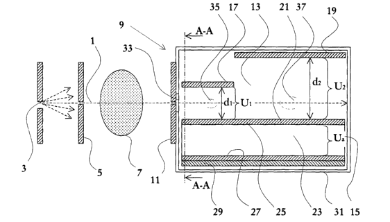
Fig. 1 is a sectional view in a plane orthogonal to the plane of
a planar X-ray beam 1 of a device for planar beam radiography,
according to an embodiment of the present invention. The device
includes an X-ray source 3, which together with a first thin
collimator window 5 produces the planar fan-shaped X-ray beam l,
for irradiation of an object 7 to be imaged. The first thin
collimator window 5 can be replaced by other means for forming an
essentially planar X-ray beam, such as an X-ray diffraction
mirror or an X-ray lens etc.
The beam transmitted through the object 7 enters a detector 9.
Optionally a thin slit or second collimator window 11, which is
aligned with the X-ray beam, forms the entrance for the X-ray
beam 1 to the detector 9.
A major fraction of the incident X-ray photons are detected in
the detector 9, which includes a chamber 13, means for electron
avalanche amplification 15, and a read-out arrangement 29. The
detector 9 is oriented such that the X-ray photons enter sideways
between a first 17, 19 and a second 21 electrode arrangement
between which a voltage U1, U=, i . e. an electric field, for drift
of electrons and ions in the chamber 13, is applied.
The first drift electrode arrangement 17, 19, is comprised of a
first 17 and a second 19 cathode plate, respectively, and the
second drift electrode arrangement is comprised of an anode plate
21. Voltage U,~ is applied between cathode plate 17 and anode
plate 21, and voltage U is applied between cathode plate 19 and
anode plate 21. U1 and U_ may be equal, but U- is preferably larger
WO 01/59480 8 PCT/SE01/00054
than U- in order to create an electric field of constant
amplitude in chamber 13. The electrode arrangements are
preferably mutually substantially parallel and separated by a
short distance dl in a first section of chamber 13, i.e. between
cathode plate 17 and anode plate 21, and by a longer distance d=
in a second section of chamber 13, i.e. between cathode plate 19
and anode plate 21. This will be discussed further below.
Chamber 13 is a conversion and drift volume and is filled with an
ionizable gas. The radiation entered into chamber 13 ionizes the
gas and the electrical field created by U1 and U, results in a
drift field in region 13 causing drift of electrons towards anode
plate 21, and thus towards avalanche amplification means 15, and
drift of ions towards cathode plates 17 and 19.
Chamber 13 is filled with a gas, which can be a mixture of for
example 90° krypton and 10~ carbon dioxide or a mixture of for
example 80o xenon and 20° carbon dioxide. The gas can be under
pressure, preferably in a range 1-20 atm. Therefore, the detector
includes a gas tight housing 31 with a slit entrance window 33,
through which the X-ray beam 1 enters the detector. The window is
made of a material, which is transparent to the radiation, e.g.
Mylar~, or a thin aluminum foil. This is a particularly
advantageous additional effect of the invention, detecting
sideways incident beams in a gaseous avalanche detector 9,
compared to previously used gaseous avalanche chambers, which
were designed for radiation incident perpendicular to the anode
and cathode plates, requiring a window covering a large area. The
window can in this way be made thinner, thus reducing the number
of X-ray photons absorbed in the window.
In operation, the incident X-rays 1 enter the detector through
the optional thin slit or collimator window 11, if present, and
between cathode plate 17 and anode plate 21, preferably in a
center plane between these as indicated in Fig. 1. The incident
X-rays 1 then travel through the gas volume in a direction
CA 02399004 2002-08-O1
WO 01/59480 9 PCT/SE01/00054
preferably substantially parallel with electrode plates 17, 19,
and 21 and get absorbed, thus ionizing gas molecules in chamber
13.
The electron avalanche amplification means 15 is arranged such
that the released electrons will drift towards and enter an
electron avalanche amplification volume 23 of amplification means
15, preferably through an avalanche cathode arrangement 25, and
wherein they will be multiplied by means of a voltage Ua being
applied between said avalanche cathode arrangement 25 and an
avalanche anode arrangement 27.
Voltage Uis applied between the avalanche cathode and the
avalanche anode such that electrons from chamber 13 passing
avalanche cathode 23 is accelerated towards avalanche anode 27,
resulting in electron multiplication and thus multiple avalanche
electrons reach avalanche anode 27. In connection with the
avalanche anode 27 a read-out arrangement 29 is provided for
detection of a pulse induced by the electron avalanches. In such
manner single-photon detection may be realized.
Preferably, the read-out arrangement 29 also constitutes the
avalanche anode electrode 27 and hence arrangements 29, 27 are
integrated into a single element. Alternatively, the read-out
arrangement 29 can be formed in connection with other parts of
electron avalanche amplification means 17 or in connection with
the drift cathode plates 17, 19. It can also be formed separated
from the anode or cathode arrangements by a dielectric layer or
substrate (not shown in Fig. 1 ) . In such a case it is necessary
that the anode or cathode arrangements is semi-transparent to
induced pulses, e.g. formed as strips or pads. With reference to
Fig. 6 different possible read-out arrangements 15 are further
discussed.
The X-ray source 3, the first thin collimator window 5, the
optional collimator window 11 and the detector 9 are connected
CA 02399004 2002-08-O1
WO 01/59480 10 PCT/SE01/00054
and fixed in relation to each other by a suitable means for
example a frame or support (not shown in Fig. 1).
The so formed device for radiography can be moved as a unit to
scan an object, which is to be examined. In a single detector
system, as shown in Fig. l, the scanning can be done by a
pivoting movement, rotating the unit around an axis through for
example the X-ray source 3 or the detector 9. The location of the
axis depends on the application or use of the device, and
possibly the axis can also run through the object 7, in some
applications. It can also be done in a translative movement where
the detector and the collimator are moved, or the object to be
imaged is moved. In a multiline configuration, where a number of
detectors are stacked, as will be explained later, in connection
with Fig. 7, the scanning can be performed in various ways. In
many cases it can be advantageous if the device for radiography
is fixed and the object to be imaged is moved.
As already mentioned, the X-rays enter the detector preferably in
a direction parallel to cathode plate 17 and anode plate 21. In
this way the detector can easily be made with an interaction path
long enough to allow a major fraction of the incident X-ray
photons to interact and be detected. The length of detector 9 and
of cathode plates 17 and 19 in a direction parallel with the
incident radiation will be further discussed below.
When an X-ray photon hits and interacts with an atom of noble
gas, a hole in the K or L shell is created, and a photoelectron
having the kinetic energy E=hv-Esr,all is released. Where inside
chamber 13 this interaction takes part is governed statistically
by the absorption rate of the X-rays in the gas or gas mixture
that is used. Fig. 2 is a diagram showing the mean free path ~, of
X-rays due to absorption in argon, Ar, krypton, Kr, and xenon,
Xe, respectively, as a function of X-ray energy by at standard
temperature and pressure (STP). In the diagram, the mean free
CA 02399004 2002-08-O1
WO 01/59480 11 PCT/SE01/00054
path varies from 0 to 70 cm as the X-ray photon energy varies
from 0 to 50 keV.
The detector in accordance with the present invention is
particularly useful when broadband X-ray radiation is used.
Hence, photoelectrons of a large range of kinetic energy are
released. Electrons having lower kinetic energy are denoted
short-range electrons, as such electrons have a rather short mean
free path, and electrons of higher kinetic energy are
correspondingly denoted long-range electrons.
A long-range electron is thus an electron with high kinetic
energy (up to 100 keV), which will travel a relatively long path
(1-20 mm at 1 atm.) before it becomes retarded and stopped
(looses its kinetic energy) in the gas. Fig. 3 is a diagram
showing the practical interaction range 8P of electrons due to
scattering in argon, Ar, krypton, Kr, and xenon, Xe,
respectively, as a function of electron energy EA at standard
temperature and pressure (STP). In the diagram, the interaction
length of the electrons varies from 0 to 5 cm as the electron
energy varies from 0 to 50 keV.
When the hole in the K or L shell is filled by an electron from a
higher level, an Auger electron and/or a fluorescent (X-ray)
photon will appear. An Auger electron is a short-range electron.
A short-range electron is an electron with low kinetic energy
(typically 1-5 keV), which will travel a relatively short path
(0.01-0.1 mm at 1 atm.) before it becomes stopped (looses its
kinetic energy) in the gas or gas mixture.
Therefore, during one single interaction of an X-ray photon with
a gas atom, e.g. Kr or Xe, several electrons will in many cases
be released simultaneously; both long-range and short-range
electrons. Further, fluorescent photons may be emitted during the
interaction.
CA 02399004 2002-08-O1
WO 01/59480 12 PCT/SE01/00054
Both long-range and short-range electrons produce electron tracks
of secondary ionized electrons produced by the electrons during
the travel in the gas. When an electron has rather high kinetic
energy (e. g. 20-30 keV), the number of released electrons
(secondary ionized electrons) is low per path unit. For electrons
having low kinetic energy (typically 1-4 keV) the number of
released electrons (secondary ionized electrons) per path unit is
higher.
As mentioned, the typical track length of a long-range electron
is about 1-20 mm at atmospheric pressure. This is therefore a
physical limit of the spatial resolution. The fluorescent photons
emitted also create ionization, as mentioned above. This
ionization takes place far away from the primary interaction with
a typical attenuation length of 1.5-250 mm at atmospheric
pressure. This ionization also deteriorates the spatial
resolution and creates background noise.
By detecting all electrons including those released from
ionization by fluorescent photons, which is done at present in
all existing gas detectors, spatial resolution is drastically
deteriorated at photon energies above 10 keV. All electrons are
detected since the electrode gap is large.
Typically between a few hundred and thousand secondary ionization
electron-ion pairs are produced from a single 20 keV X-ray photon
in this process. The secondary ionization electrons (together
with the primary ionization electron) will drift towards the
electron avalanche amplification means 17 due to the electric
field in the conversion and drift volume 13. When the electrons
enter regions of focused field lines of the electron avalanche
amplification means 17 they will undergo avalanche amplification.
The movements of the avalanche electrons and ions induce
electrical signals in the read-out arrangement 29 for detection
of electron avalanches. The read-out arrangement 29 is preferably
arranged in vicinity of electron avalanche anode 27, but the
CA 02399004 2002-08-O1
WO 01/59480 13 PCT/SE01/00054
signals may be picked up elsewhere, such as e.g. close to cathode
plates 17 and 19 or at avalanche cathode 25, or at a combination
of two or more of said locations. The signals are further
amplified and processed by read-out circuitry (not shown in Fig.
1) to obtain accurate measurements of the X-ray photons. The
read-out arrangement 29 is arranged such that electron avalanches
derivable mainly from ionization in the respective chamber
section (i.e. between cathode plate 17 and anode plate 21, e.g.
at 35, and between cathode plate 19 and anode plate 21, e.g. at
37) are separately detectable. Hence, a detector 9 for energy
resolved detection of X-rays is achieved, wherein, at least from
a statistical viewpoint, X-rays of lower energies are absorbed in
the first section of chamber 13 having a short distance dl
between the electrode plates and X-rays of higher energies are
absorbed in the second section of chamber 13 having a distance d
between the electrode plates.
The electrode distance di in the first chamber section is
preferably chosen such that detection of lower energy photons of
high spatial resolution is enabled. Thus, dl shall preferably be
shorter than the attenuation length of the fluorescent (X-ray)
photons. This results in that a great number of fluorescent
photons will not cause ionization in the conversion and drift
volume.
A further improvement of the spatial resolution is achieved if
the detector is provided with a first chamber section having an
electrode gap distance di, which is shorter than the length of
the electron tracks (i.e. the interaction length) of long-range
electrons. This results in that an even larger number of
fluorescent photons and a large number of long-range electrons
will not undergo full energy loss in the first chamber section.
The distance dl may preferably be selected such that a major
portion of the fluorescent photons and/or long-range electrons
are discriminated. That is, a major portion of the fluorescent
CA 02399004 2002-08-O1
WO 01/59480 14 PCT/SE01/00054
photons will not cause ionization in the conversion and drift gap
and/or a major portion of the long-range electrons will not be
retarded to the energy level where they produce a high number of
secondary ionized electrons per path unit within the first
chamber section.
Still a further improvement of the spatial resolution is achieved
if the detector is provided with a first chamber section having
an electrode gap distance dl, which is essentially a few times
the length of the electron tracks (i.e. interaction length) of
short-range electrons, e.g. 1-5 times the length of the electron
tracks of the short-range electrons. This results in that a
larger number of fluorescent photons and a larger number of long-
range electrons will not undergo full energy loss in the
conversion and drift volume. Of course the distance dl can be
smaller than the length of the electron tracks of the short-range
electrons, but then the efficiency will go down since also short-
range electrons will reach the electrode plates before complete
ionization.
By such geometrical discrimination of long-range electrons and
fluorescent photons it is achieved that a larger amount of the
detected avalanches are caused by short-range electrons, than
without the discrimination. This improves the spatial resolution
since the long-range electrons and fluorescent photons cause
avalanches far from the interaction position of the incident X-
ray. The more long-range electrons and fluorescent photons that
are discriminated, the higher the ratio between detected
avalanches caused by short-range electrons and detected
avalanches caused by long range electrons and fluorescent photons
will be. A higher spatial resolution is hereby achieved.
The length 11 of the first chamber section in the direction of
the incident X-rays is arranged such that a substantial portion
of the lower energy radiation is absorbed in the first chamber
section.
CA 02399004 2002-08-O1
WO 01/59480 15 PCT/SE01/00054
The electrode distance d- in the second chamber section is
preferably chosen such that detection of higher energy photons is
enabled. Thus, d= shall preferably be substantially longer than
dl in order to allow primary long-range electrons to be retarded
and to ionize gas molecules, thus releasing shorter-range
electrons. The efficiency of detecting higher energy photons is
thus improved to the cost of a deteriorated spatial resolution.
Preferably though, the electrode distance d- in the second
chamber section is shorter than the attenuation length of the
fluorescent (X-ray) photons. This results in that a great number
of fluorescent photons will not cause ionization in the
conversion and drift volume.
A further improvement of the spatial resolution is achieved if
the detector is provided with a second chamber section having an
electrode gap distance d~, which is essentially a few times the
length of the electron tracks (i.e. interaction length) of long-
range electrons, e.g. 1-5 times the length of the electron tracks
of the long-range electrons.
The length 1_ of the second chamber section in the direction of
the incident X-rays is arranged such that a substantial portion
of the higher energy radiation is absorbed in the second chamber
section.
Certainly, the electrode distances dl and d=, and the chamber
section lengths 11 and 1- are chosen for each particular
application and for each particular radiation spectrum used in
order to achieve desired detection efficiency, and required
spatial and energy resolution.
Also electronic discrimination can be used to improve the spatial
resolution and the energy resolution. As mentioned, short-range
electrons produce a high number of secondary ionized electrons
per path unit, and electrons having high energy produce a low
number of secondary ionized electrons per path unit. Therefore
CA 02399004 2002-08-O1
WO 01/59480 16 PCT/SE01/00054
the avalanche-amplified pulses at the read-out arrangement are
high and/or wide for short-range electrons, while they are small
for a long-range electron in the first chamber section. By
providing the read out electronics with a threshold function as
regards some suitable signal derived parameter, e.g. amplitude or
integrated value, the pulses from the long-range electrons in the
first chamber section can be electronically discriminated and
hence both the spatial resolution and the energy resolution are
further improved.
Similarly, in the second chamber section, the high-energy
electrons are allowed to be fully retarded, and hence in total a
larger number of electrons is released from such electrons than
from short-range electrons and therefore the detected avalanche
amplified pulses are higher and/or wider for longer-range
electrons than for shorter-range electrons. Thus, as higher
energy photons produce longer-range electrons the energy
resolution in the second chamber section may be further improved
by electronically discriminating pulses having a signal-derived
parameter, e.g. amplitude or integrated value, below a certain
threshold value.
In yet another embodiment of the present invention the first and
second chamber sections are separated in a fluid-tight, but
radiation permeable, manner (not shown in fig. 1) and each
chamber is individually filled with an ionizable gas of a
predetermined pressure. The chamber sections may be separated by
a fluid-tight wall in which a suitable radiation transparent
window is arranged (similar to window 33), through which window
the X-ray beam 1 enters the second chamber section. By
controlling the content of the gas mixture and the gas pressure
in each chamber individually a further improved energy and
spatial resolution may be achieved.
With reference now to Fig. 4 a particular embodiment of the
present invention is to be described, wherein it can be used to
CA 02399004 2002-08-O1
WO 01/59480 1 ~ PCT/SE01/00054
measure the bone mineral density of humans. Fig. 4 is a diagram
showing the absorption coefficient a, of X-rays due to absorption
in tissue, and in bone, respectively, of human body as a function
of X-ray energy. In the diagram, the absorption coefficient
varies from 1 to roughly 0.4 as the X-ray photon energy varies
from 0 to 150 keV. Shown is also the differential absorption
coefficient (indicated Tissue-Bone), which is an indication of
the absorption selectivity between tissue and bone, as a function
of the photon energy.
Normally the bone is surrounded by an unknown amount of tissue.
One commonly used method to estimate the amount of bone is to
detect transmitted X-rays at two different X-ray energies. One
exposure is made at X-ray energies where bone and tissue absorb
X-rays very differently; typically at 40 keV where the
differential absorption coefficient has a maximum, see Fig. 4.
Another exposure is made at energies where bone and tissue absorb
X-rays in a similar way; typically at energies above 100 keV, see
Fig. 4 again. From these two measurements the amount of bone is
estimated. However, this requires that the detector is capable of
detecting low energy (around 40 keV) X-rays as well as high
energy X-rays (>100 keV), which is often a problem. Furthermore,
to obtain beams with a narrow energy distribution at low energy,
the incoming X-ray flux, which has a broad spectrum, needs to be
heavily filtered, putting a large load on the X-ray tube. The two
separate exposures, taken at different times, also give rise to
problems due to movements of the object between the two
exposures.
The present invention describes a detector and a method that can
measure X-rays over a wide energy range. Low energy X-rays are
preferably detected in the first, thin chamber section of the
detector due to their short absorption length. High energy X-rays
mainly traverse the first chamber section of the detector and are
detected in the second, thicker chamber section. The invention
allows the same detector to be used to efficiently detect X-rays
CA 02399004 2002-08-O1
WO 01/59480 18 PCT/SE01/00054
at rather different energies with the same detector, using the
commonly used double exposure method.
Alternatively, the two measurements can be made simultaneously
using a broad X-ray spectrum of the incident X-rays. This second
alternative requires less filtering of the X-rays and put less
load on the X-ray tube. Furthermore, by simultaneously detecting
the two energy intervals problems of movements between exposures
are reduced.
Fig. 5 shows a schematic, partly enlarged, cross sectional view
of a particular embodiment of the invention, taken along A-A of
Fig. l, and shows particularly the avalanche amplification means
in more detail. It shall, however, be appreciated that the
present invention is not limited to such a design. Other possible
avalanche amplification means designs are further elaborated in
our copending Swedish patent application No. 9901325-2 entitled
Radiation detector, an apparatus for use in planar radiography
and a method for detecting ionizing radiation and filed on April
14, 1999, which application hereby is incorporated by reference.
It shall also be appreciated that the avalanche amplification
means may be a solid-state device or comprise a liquid
amplification region.
The first electrode arrangement 17 comprises a dielectric
substrate 41 and a conductive layer 43 being a cathode electrode,
and the second electrode arrangement 21 being the same
arrangement as the avalanche cathode 25. The avalanche anode 27
comprises a dielectric substrate 45 and conductive layer strips
47.
A dielectric 49 is arranged between the avalanche cathode 25 and
the avalanche anode 27. This could be a gas or a solid substrate
49 carrying the cathode 25 and the anode 27, as shown in the
Figure. A first voltage is applied between arrangement 17 and
arrangement 21, 25 by means of a DC power supply (not shown in
Fig. 5) and a second voltage is applied between cathode 25 and
CA 02399004 2002-08-O1
WO 01/59480 19 PCT/SE01/00054
anode 27 such that an electric field 51 is achieved, which is
very strong in gas-filled avalanche amplification regions 53. The
avalanche regions 53 are formed in a region between and around
the edges of the avalanche cathode 25 which are facing each
other, and between the avalanche cathode 25 and the avalanche
anode 27, where a concentrated electric field will occur due to
the applied voltages.
The voltages applied are selected so that a weaker electric
field, drift field, is created over the first section of chamber
13. Electrons (primary and secondary electrons) released by
interaction, e.g. at 35, will drift, due to the drift field,
towards the avalanche amplification means. They will enter the
very strong avalanche amplification field and be accelerated. The
accelerated electrons will interact with other gas atoms in one
of regions 53, causing further electron-ion pairs to be produced.
Those produced electrons will also be accelerated in the field,
and will interact with new gas atoms, causing further electron
ion pairs to be produced. This process continues during the
travel of the electrons in the avalanche region towards the anode
27 and an electron avalanche is formed.
The avalanche regions 53 are formed by openings or channels in
cathode 25 and the dielectric substrate 49, if present. The
openings or channels can be of arbitrary shape, e.g. circular or
square, as seen from above, or continuous, longitudinal extending
between two edges of the substrate 49, if present, and cathode
25. In the case the openings or channels are circular when seen
from above they are arranged in rows, each row of openings or
channels including a plurality of circular openings or channels.
A plurality of longitudinal openings or channels or rows of
channels are formed beside each other, parallel with each other
or with the incident X-rays. Alternatively, the openings or
channels can be arranged in other patterns.
CA 02399004 2002-08-O1
WO 01/59480 2 0 PCT/SE01/00054
Conductive layer strips 47 also forms read-out elements of read-
out arrangement 29. The strips are arranged in connection with
the openings or channels forming the avalanche regions 53.
Preferably one strip is provided for each opening or channel or
row of openings or channels. The strips could be divided into
sections along its length, where one section could be provided
for each opening or channel or for a plurality of openings or
channels, in the form of pads, see further discussion below. The
strips and the sections, if present, are electrically insulated
from each other. Each detector electrode element i.e. strip or
section is preferably separately connected to processing
electronics (not shown in Fig. 5).
By providing a plurality of readout strips 47 as shown in Fig. 5
a detector 9 is achieved, wherein electron avalanches derivable
mainly from ionization by transversely separated portions of the
planar radiation beam are separately detectable. Hereby, one-
dimensional imaging may be performed using detector 9.
Alternatively the read-out elements can be located on the
backside of the substrate. In this case it is necessary that the
anode electrodes 4, 19 are semi-transparent to induced pulses. In
connection with Fig. 6 below different possible arrangements of
read-out elements are shown.
As an example, the longitudinal channels can have a width in the
range 0.01-1 mm, the channels can have a width in the range 0.01-
1 mm, and the thickness of the dielectric 49 (separation between
avalanche cathode 25 and anode 27) is in the range 0.01-1 mm.
Alternatively, conductive layers 43 and 47 can be replaced by a
resistive carrier of e.g. silicon, conductive glass or diamond,
and dielectric substrates 41 and 45 can be replaced by conductive
layers.
A cross-sectional view taken parallel with A-A in Fig. 1, but in
the second section of chamber 13 would be identical to the one
CA 02399004 2002-08-O1
WO 01/59480 21 PCT/SE01/00054
shown in Fig. 5, except of that the gap constituting chamber 13
would be considerably larger. By providing separate readout
strips beneath the respective sections of chamber 13 a detector 9
is achieved, wherein electron avalanches derivable mainly from
ionization by X-rays of different energy are separately
detectable.
In the embodiment described above particular locations of the
detector anode and cathode arrangements have been described.
There are, however, a plurality of other locations that are
equally well suitable in connection with the present invention.
Referring now to Fig. 6, a possible configuration of an avalanche
anode arrangement 27 (and read-out arrangement 29) is shown. The
arrangement is formed by conductive strips 47 and 63.
A plurality of strips 47 are placed side by side and a plurality
of strips 63 are placed side by side, the strips 47, 63 extending
in directions parallel to the direction of incident X-ray photons
65, originating from source 3, at each location. Preferably,
strips 47 are arranged beneath the first section chamber and
strips 63 are arranged beneath the second chamber section. The
strips are formed on a substrate, electrically insulated from
each other, by leaving a space between them (not shown in Fig.
6). The strips may be formed by photolithographic methods or
electroforming, etc.
The space and the width of the strips 47 are adjusted to the
specific detector in order to obtain the desired (optimal)
spatial resolution. Thus, strips 63 are wider than strips 47, as
the spatial resolution achievable anyhow is worse for the higher-
energy X-rays.
The strips 47 should be placed under the openings or channels or
rows of openings or channels as shown in Fig. 5. Similarly,
strips 63 should be placed under corresponding openings or
CA 02399004 2002-08-O1
WO 01/59480 22 PCT/SE01/00054
channels or rows of openings or channels formed in the avalanche
amplification means beneath the second chamber section.
Each of the strips 47, 63 is connected to the processing
electronics (not shown in Fig. 6) by means of a separate signal
conductor, where the signals from each strip preferably are
processed separately. If anode or cathode strips constitute the
detector strips, the signal conductors also connects the
respective strip to the high voltage DC power supply, with
suitable couplings for separation.
As indicated in Fig. 6, the strips 47, 63 are aiming at the X-ray
source 3, which provides compensation for parallax errors in
detected images.
In the case the read-out arrangement 29 is a separate
arrangement, the anode electrode 27 can be formed as a unitary
electrode without strips and spacings.
An alternative configuration of a read-out arrangement (not
illustrated) has the strips 47 and/or 63 further divided into
segments in the direction of the incident X-rays, the segments
being electrically insulated from each other. Preferably a small
spacing extending perpendicular to the incident X-rays is
provided between each segment of respective strip. Each segment
is connected to the processing electronics by means of a separate
signal conductor, where the signals from each segment preferably
are processed separately.
This read-out arrangement can be used when further energy
resolved detection of the X-rays is required. By statistical
methods one can restore the spectrum of the incident photons with
good energy resolution. See for example E.L. Kosarev et al.,
Nucl. Instr and methods, 208 (1983) 637, and G.F. Karabadjak et
al., Nucl. Instr and methods, 217 (1983) 56.
CA 02399004 2002-08-O1
WO 01/59480 2 3 PCT/SE01/00054
Generally for all embodiments, each incident X-ray photon causes
one induced pulse in one (or more) detector electrode element.
The pulses are processed in the processing electronics, which
eventually shapes the pulses, and integrates or counts the pulses
from each strip (pad or sets of pads) representing one picture
element. The pulses can also be processed so as to provide an
energy measure for each pixel.
Where the detector electrode is on the cathode side, the area of
an induced signal is broader (in a direction perpendicular to the
direction of incidence of the X-ray photons) than on the anode
side. Therefore, weighing of the signals in the processing
electronics is preferable.
Fig. 7 shows schematically a device 91 according to an embodiment
of the present invention having a plurality of the inventive
detectors 9 stacked, side-by-side of each other. By this
embodiment multiline scan can be achieved, which reduces the
overall scanning distance, as well as the scanning time. The
device of this embodiment includes an X-ray source 3, which
together with a number of collimator windows 5 produce a number
of planar fan-shaped X-ray beams l, for irradiation of the object
7 to be imaged. The beams transmitted through the object 7
optionally enter the individual stacked detectors 9 through a
number of second collimator windows 11, which are aligned with
the X-ray beams. The first collimator windows 5 are arranged in a
first rigid structure (not shown in Fig. 7), and the optional
second collimator windows 11 are arranged in a second rigid
structure (not shown in Fig. 7) attached to the detectors 9, or
arranged separately on the detectors.
The X-ray source 3, the first rigid structure, and the possible
second rigid structure including collimator windows 11,
respectively, and the stacked detectors 9, which are fixed to
each other, are connected and fixed in relation to each other by
a certain means, e.g. a frame or support (not shown in Fig. 7).
CA 02399004 2002-08-O1
WO 01/59480 2 4 PCT/SE01/00054
The so formed device for radiography can be moved as a unit to
scan an object, which is to be examined. In this multiline
configuration, the scanning can be done in a transverse movement,
perpendicular to the X-ray beam, as mentioned above. It can also
be advantageous if the device for radiography is fixed and the
object to be imaged is moved. Alternatively, the collimator and
the detector can be moved synchronously by a commonly controlled
motor.
A further advantage of using a stacked configuration, compared to
large single volume gas detectors, is reduction of background
noise caused by X-ray photons scattered in the object 7. These
scattered X-ray photons travelling in directions not parallel to
the incident X-ray beam could cause "false" signals or avalanches
in one of the other detectors 9 in the stack, if passing through
anode and cathode plates and entering such a chamber. This
reduction is achieved by significant absorption of (scattered) X-
ray photons in the material of the anode and the cathode plates,
or the collimator 11.
This background noise can be further reduced by providing thin
absorber plates (not illustrated) between the stacked detectors.
These absorber plates or sheets can be made of a high atomic
number material, for example tungsten.
It is general for all embodiments that the gas volumes are very
thin, which results in a fast removal of ions, which leads to low
or no accumulation of space charges. This makes operation at high
rate possible.
It is also general for all embodiments that the small distances
leads to low operating voltages, which results in low energy in
possible sparks, which is favorable for the electronics.
The focusing of the field lines in the embodiments is also
favorable for suppressing streamer formations. This leads to a
reduced risk for sparks.
CA 02399004 2002-08-O1
WO 01/59480 2 5 PCT/SE01/00054
As an alternative for all embodiments, the electric field in the
conversion and drift gap (volume) can be kept high enough to
cause electron avalanches, hence to be used in a pre-
amplification mode.
As a further alternative, the electrode arrangement 21, 25 may be
dispensed with, and an electric field between electrode
arrangement 17, 19 and cathode arrangement 27 can be kept high
enough to cause electron avalanche amplification within the
complete volume as defined by regions 13 and 23, 53.
Further, all electrode surfaces may be covered by a resistive
material in order to decrease the risk for occurrence of sparks,
which will influence the measurement and may destroy electronic
equipment of the detector. Such resistive layers are further
described in our copending Swedish patent application No.
9901327-8 entitled Radiation detector and an apparatus for use in
radiography and filed on April 14, 1999. The application is
hereby incorporated by reference.
It will be obvious that the invention may be varied in a
plurality of ways. For example, the voltages can be applied in
other ways as long as the described electrical fields are
created.
Such variations are not to be regarded as a departure from the
scope of the invention. All such modifications as would be
obvious to one skilled in the art are intended to be included
within the scope of the appended claims.
CA 02399004 2002-08-O1