Note: Descriptions are shown in the official language in which they were submitted.
CA 02399027 2002-07-31
WO 01/56771 PCT/CHO1/00070
-1-
METHOD FOR FABRICATING MICRO-STRUCTURES WITH
VARIO~TS SURFACE PROPERTIES IN MULTILAYER BODY
BY PLASMA ETCHING
FIELD OF THE INVENTION
The present invention provides a fabrication method for the three dimensional
structuration and patterning of at least two different surface properties for
micro-
systems or micro-substrates.
BACKGROUND OF THE INVENTION
Over the last ten years, a general effort towards miniaturization of the
analytical tools
has been observed. Two main reasons are pushing the development miniaturized
chemical apparatus, which have been called Micro Total Analysis Systems (p-
TAS):
a decrease of analyte consumption and a decrease of duration of single
analysis. Both
needs are particularly evident in the new development of life science, where
genetic
analysis and high throughput screening in drug discovery take more and more
importance. In these applications, the reason for limiting the analyte
consumption are
evidenced by the increasing number of performed assays. In this case, the use
of
reactants for analysis must be as small as possible in order not only to
reduce the
CA 02399027 2002-07-31
WO 01/56771 PCT/CHO1/00070
-2-
cost but also to limit the waste production. In other cases, the analysis of
extremely
small volumes is required. Such a volume may be only a few nL, e.g. in the
case of
neurological fluid analysis or in prenatal diagnostics. In many cases, the
decrease in
analysis time is also an important issue e.g. in medical diagnostics, where
the time
factor may signify a fatal issue for the patient. Two different and
complementary
strategies have been developed in parallel to achieve these goals. On one
hand, the
fabrication of microfluidic devices has allowed fluid handling in pL volumes
and, on
the other hand, immobilization of affinity reagents into high density 2-
dimensional
arrays for high throughput affinity analysis.
In recent years, capillary electrophoretic methods have enjoyed gaining
popularity,
primarily due to the observed high separation efficiencies, peak resolution,
and wide
dynamic ranges of molecular weights that may be analyzed. Furthermore, the
simple
open-tubular capillary design has lead itself to a variety of automation,
injection and
detection strategies developed previously for more conventional analytical
technologies.
The general instrumental set-up involves a capillary filled with an
electrolyte
solution and a high voltage power supply connected to electrodes in contact
with
small fluid filled reservoirs at either end of the capillary. The power supply
is
operated in order to apply an electric potential field tangential to the
capillary
surface, in the range of 100-1000 V/cm. When the potential is applied,
migration
processes occur. The electric field imposes a force onto charged species
leading to
the electrophoretic migration of sample molecules within the capillary.
Furthermore,
when file capillary surface is charged, a flow of the whole solution is
induced by
electro-osmosis. Therefore, electrophoresis is in most cases superimposed on a
so-
called electroosmotic flow (EOF). Species moving in the capillary as a result
of these
forces will then be transported past a suitable detector, absorbance and
fluorescence
CA 02399027 2002-07-31
WO 01/56771 PCT/CHO1/00070
-3-
being the most common. Capillary electrophoresis has been applied to numerous
analytes spanning pharmaceutical, environmental and agricultural interests. A
common focus amongst these activities is bioanalysis. Separation methods are
developed for peptide sequencing, amino acids. isoelectric point determination
for
proteins, enzyme activity, nucleic acid hybridization, drugs and metabolites
in
biological matrices and affinity techniques such as immunoassays. Furthermore,
buffer additives such as cyclodextrins and micellar phases have added the
ability to
perform chiral separations of biologically active enantiomers of tryptophan
derivatives, ergot alkaloids, epinephrines and others which is of great
interest to the
pharmaceutical industry.
The capillaries described above generally have internal diameters between 50-
200
p.m and are formed in fused silica. The microfabrication of capillaries has
also been
accomplished by machining directly onto planar, silicon-based substrates.
Silicon
substrates have an abundance of charged silanol groups and thus generate
considerable EOF. In the case of micromachining, EOF can be an advantage in
that
the flow of the bulk solution can be used for many liquid handling operations.
There
has recently been intense activity in the area of chemical instrumentation
miniaturization. Efforts have been made to reduce whole laboratory systems on
to
microchip substrates, and these systems have been termed micro-Total
Analytical
Systems (~-TAS). As already mentioned, most of such ~.-TAS devices to date
have
been produced photolithographicly on silicon-based substrates. This process
involves
the generation of the desired pattern on a mask, through which a photoresist
coated
silicon dioxide wafer is exposed to light. Solubilised photoresist is then
removed and
the resulting pattern anisotropically etched with hydrofluoric acid. Etched
capillaries
are then generally sealed by thermal bonding with a glass covert. The bonding
technique in particular is labour and technology intensive and thermal bonding
requires temperatures between 600-1000 °C. This bonding technique has a
very low
tolerance of defect or presence of dust and requires clean room conditions for
the
CA 02399027 2002-07-31
WO 01/56771 PCT/CHO1/00070
-4-
fabrication, which means that the production is very expensive. Alternative
fabrication techniques have also been developed based on organic polymers.
Fabrication of polymer microfluidic devices has been shown by injection
moulding
or polymerising polydimethyl siloxane (PDMS) on a mould These two techniques
have the advantage to replicate a large number of micro-structures with the
same
pattern given by the mould. Other techniques based on electromagnetic
radiation
either for polymerisation under X-ray (LIGA) or for ablation have also been
recently
shown to be feasible. This last fabrication technique allows fast prototyping
by
writing pattern on a substrate that can be moved in the X and Y directions.
Different
structures can then be fabricated just by moving the substrate in front of the
laser
beam.
As already mentioned, electroosmotic pumping is used here not only to separate
samples but also to dispense discrete amounts of reactives or to put in
contact
solutions for the reaction in continuous flow systems. A large diversity of
structures
and electrical connections have been presented which permit to deliver and
analyse
samples in less than a millisecond by electrophoresis for example.
This spectacular property also evidences that, in these microchannels, the
main
transport mechanism between two flowing solutions is diffusion. As different
species
exhibit different diffusion coefficients, efficient mixing becomes
problematic, and
this is often presented as a serious limitation for the wider use of
microfluidic in total
analysis systems. In order to solve this problem, mixers have been presented,
where
the flows are for instance divided in smaller channels (20 p,m) before being
placed in
contact. In this manner, the diffusion time is reduced and hence the mixing
efficiency
enhanced.
CA 02399027 2002-07-31
WO 01/56771 PCT/CHO1/00070
-$-
Many recent advances in chemical analysis have involved the incorporation of
biomolecules capable of selective and high affinity binding to analytes of
interest.
Such devices are often termed biosensors, which involve real-time transduction
of
the binding event into an electronic signal, but also include analytical
technology
consisting of immunoassays, enzyme reaction, as well as nucleic acid
hybridisation:
Bio-analytical devices utilising this technology have been applied to a wide
range of
applications in medicine agriculture, industrial hygiene, and environmental
protection. Enzyme electrodes represent the oldest group of biosensors and are
being
increasingly used for clinical testing of metabolites such us glucose,
lactate, urea,
creatinine or bilirubin. Several groups have developed needle-type electrodes,
for
subcutaneous glucose measurements. A microelectrochemical enzyme transistor
has
been developed for measuring low concentrations of glucose. Efforts continued
towards other clinically relevant metabolites particularly for the multiple-
analyte
determination. Strategy to incorporate affinity steps is also an active area
of
biosensors. The emerging area of DNA hybridisation biosensors has been a very
popular topic for the clinical diagnosis of inherited diseases and for the
rapid
detection of infectious microorganisms.
Recent interest in the development of miniaturised, array-based multianalyte
binding
assay methods suggests that the ligand assay field is on the brink of a
technological
revolution. The studies in this area have centered largely on antibody or DNA
spot
arrays localised on microchips which are potentially capable of determining
the
amounts of hundreds of different analytes in a small sample (such as a single
drop
blood). Array-based immunoassay methods shows the particular importance in
areas
such as environmental monitoring where the concentrations of many different
analytes in test samples are required to be simultaneously determined.
Affymetrix
developed ways to synthesise and assay biological molecules in a highly dense
parallel format. Integration of two key technologies forms the cornerstone of
the
method. The first technology, light-directed combinatorial chemistry, enables
the
CA 02399027 2002-07-31
WO 01/56771 PCT/CHO1/00070
-6-
synthesis of hundreds of thousands of discrete compounds at high resolution
and
precise locations on a substrate. The second laser confocal fluorescence
scanning
permits measurement of molecular interactions on the array.
Recently, the Laboratoire d'Electrochimie of the EPFL Lausanne has presented a
patterning technique based on the photoablation process. In order to fabricate
microarrays of proteins, the polymer substrate is firstly blocked with a
bovine serum
albumin (BSA) layer avoiding non specific adsorption of protein on the
substrate
layer. Microspots are then created on the surface by photoablation of the BSA
layer,
on which avidin can be adsorbed yet. This micropatterning technique allows
then to
specifically adsorb antibodies linked to biotin on the avidin spots as
visualised by
biotin-fluorescein complex.
Apart from electrophoretic separations and hybridisation, an increasing number
of
applications on p.-TAS have been shown in the Iast few years. FuII DNA
analysers
have been implemented in a single device with a polymerised chain reaction
(PCR)
chamber followed by an electrophoretic separation. Continuous flow PCR has
also
been shown where the analyte solution is driven through a capillary crossing
zones of
different temperature. Other genetic analysis have also been demonstrated
comprising high speed DNA sequencing, high density parallel separation or
single
DNA molecule detection. Another application of p,-TAS has been shown in
electrochromatography. An open-channel electrochromatography in combination
with solvent programming has been demonstrated using a microchip device.
Others
have successfully used ~-TAS to conduct immunoassays involving competitive
markers, noting several advantages over more traditional formats including (a)
high
efficiency separations between competitive markers and antibody-marker
complexes,
(b) excellent detection limits (0.3-0.4 amol injected) at high speed, and (c)
good
potential for automation. This has first been demonstrated in a micromachined
CA 02399027 2002-07-31
WO 01/56771 PCT/CHO1/00070
capillary electrophoresis device by, Koutny et al. Cortisol was determined in
serum
using a competitive immunoassay that was subsequently quantitated using ~.-
TAS. A
microfluidic system was fabricated on a glass chip to study mobilisation of
biological
cells on-chip. Electroosmotic and/or electrophoretic pumping were used to
drive the
cell transport within a network of capillary channels. An automated enzyme
assay
was performed within a microfabricated channel network. Precise concentrations
of
substrate, enzyme and inhibitor were mixed in nanoliter volumes using
electrokinetic
flow. Finally, the new insight in the use microfabricated system has been to
combine
the advantage of parallel reactions and liquid handling in extremely small
volumes
IO with an electrospray or nanospray interface for mass spectrometry analysis.
This last
application opens a way to efficiently use the microchip format not only for
genetic
analysis where it is already recognised but also in protein sequencing.
Several microfabrication processes have been shown that modify the surface
properties of the polymer.
It is known that reactions of gas plasmas with polymers can be classified as
follows:
1. Surface reactions:
Reactions between the gas-phase species and surface species produce
functional groups and/or crosslinking sites at the surface.
2. Plasma polymerisation:
The formation of a thin film on the surface of a polymer via polymerisation of
an organic monomer such as CHd, C2H6, C2F4 arid C3F6 m a plasma.
CA 02399027 2002-07-31
WO 01/56771 PCT/CHO1/00070
_$_
3. Cleaning and etching:
Materials are removed from a polymer surface by chemical reactions and
physical etching at the surface to form volatile product.
Patent of particular relevance in the etching process:
US 5099299 (Dyconex)
Patent vrith particular relevance in lamination sealing of polymer micro-
structure:
WO 991197 17 (Aclara Biosciences)
Patent of particular relevance in patterning of properties:
WO 9823957 A(EPFL)
Other patents on microfabrication and fluidic control by surface properties:
WO 9823957 A(EPFL)
WO 9846439 (Caliper technology)
CA 02399027 2002-07-31
WO 01/56771 PCT/CHO1/00070
-9-
WO 9807019 (Gamera Bioscience)
SUMMARY OF THE INVENTION
According to the present invention, an etching method for manufacturing micro-
structures or openings in a multilayer body made of selected materials is
provided,
wherein the surface properties of the layers are controlled individually and
preferably
simultaneously control, so that conduits, grooves, reservoirs, holes and so
forth are
formed and exhibit various surface properties allowing further
functionalisation of
selected surfaces as well as fluid handling.
Further, an etching method of the above kind is provided where the conduits
and
reservoirs are manufactured in sequential etching steps between which selected
layers can be removed or added to the multilayer body or between which the
properties of selected etched surfaces can be modified.
Still further, such an etching method is provided for manufacturing micro-
structures
or openings in a multilayer body which can contain a selected sequence of
insulating
and optically or electrically conductive layers, whereby measurement and/or
detection of one or more analytes and/or fluid handling means are provided.
Also, such an etching method is provided where a plurality of layers are
manufactured simultaneously or where etching processes are used.
CA 02399027 2002-07-31
WO 01/56771 PCT/CHO1/00070
-10-
Thus, the present invention provides a fabrication method for the three
dimensional
structuration and patterning of at least two different surface properties for
micro-
systems.
The invention further comprises products manufactured using this method as
defined
in the claims.
The technology is based on the anisotropic plasma etching of organic polymer
sheets
partially protected by a metallic mask. The originality of the process is to
pattern the
surface properties by the same physical means as the one used for the three
dimensional fabrication and simultaneously to this fabrication. Surface
properties
mean, but are not limited to hydrophobicity hydrophilicity, conductivity,
reflectability, rugosity and more precisely the chemical and/or physical state
of the
surface. It is also possible to generate the desired fonctionalities, for
instance
carboxylic acid, ester, ether, amid or imid, during the etching process. The
patterning
of the different properties may be achieved by two different techniques that
may be
used separately or simultaneously.
1. The fabrication of multilayer of polymer of different properties, for
example,
a sandwich composed of two thin layers of electrical insulator (polystyrene)
spin coated on both sides of a conducting polymer sheet (carbon filled
polystyrene). The plasma etching cuts vertically the three layers, letting
appearing a band of conducting band isolated by two others.
2. The substrate partially protected by a mask on both sides is placed in the
middle of two chambers (A and B), separated hermetically, inside which a
plasma is generated differently in chamber A than in chamber B. For this,
CA 02399027 2002-07-31
WO 01/56771 PCT/CHO1/00070
-11-
the surface exposed to chamber A is treated with an oxidative plasma (02)
while the other one with a non-oxidative plasma (N2). The surface of such a
hole would be half hydrophilic and half hydrophobic with respect to the
etching rate of both plasma.
In a preferred embodiment, the technology may be applied to. manufacture micro-
analytical systems that are devoted to many applications, like for instance
chemical
and biological analysis, synthesis and/or separation. Furthermore, in another
embodiment, the technology may serve to manufacture devices devoted to
reactions
occurring at the interface between a liquid and a solid surface or at the
interface
between two solutions.
For example, microelectrodes or micro-needles may be fabricated and used for
electrochemical detection or in mass spectrometry sampling. The system may be
used for liquid extraction between two phases like partitioning experiments.
Furthermore, the technology may be applied to every kind of induced flow like
diffusion, convection (for example by electroosmosis) or migration (for
example by
electrophoresis). The technology may also be used for applications where the
plasma
created surface is chemically or biochemically derivated in order to perform
chemical or biochemical assays. As further example, the technology may be
applied
to reaction types where the temperature may be adjusted and/or controlled for
instance by the use of electrical means like integrated thermistors or
thermocouples,
as for example for PCR reactions.
BRIEF DESCRIPTION OF THE DRAWINGS
CA 02399027 2002-07-31
WO 01/56771 PCT/CHO1/00070
- 12-
Fig. lA-lE show schematic sectional views through a portion of an embodiment
of the multilayer body showing methods for manufacturing micro-
structures or openings in this multilayer body which is coated on both
sides and which is made of a plurality of materials,
Fig. 2A-2E show schematic sectional views, through a portion of an embodiment
of the multilayer body showing methods for manufacturing micro-
structures or openings in this multilayer body which is coated on both
sides and which is made of a plurality of materials, one of the layers
already containing micro-structures or openings,
Fig. 3A-3C show schematic sectional views through a portion of an embodiment
of the multilayer body showing methods for manufacturing micro-
structures or openings in this multilayer body made of a plurality of
materials using a plurality of etching processes allowing to process
one layer and to remove another one simultaneously,
Fig. 4A-4C show schematic sectional views through a portion of an embodiment
of the multilayer body flowing methods for manufacturing micro-
structures or openings in a multilayer body made of a plurality of
materials, using a plurality of etching processes allowing to
discriminate the structuration of two different portions of a layer,
Fig. 5 is a schematic diagram showing a method for processing a plastic film
of indeterminate length in accordance with the present invention,
CA 02399027 2002-07-31
WO 01/56771 PCT/CHO1/00070
-13-
Fig.6A-6E schematically show a sequence of microfabrication with plasma
etching,
Figs. 7A-7C show a side view of micro-structures fabricated by plasma etching
with the electrodes and the lamination,
Fig. 8 is a top view of the unsealed micro-structure, together with closer
views of the electrode microdisk inserted in the microchannel,
Fig. 9A shows the voltammetric detection of ferrocene carboxylic acid in the
microchannel in three electrode mode versus Ag/AgC1 (ferrocene
carboxylic acid concentration from 0 to 500 ~.M in 125 mM PBS pH
7.4 + KCl 100 mM),
Fig.9B represents the ferrocene carboxylic acid concentration versus the
current at 400 mV vs. Ag;AgCl,
Fig. 10 shows the voltammetric detection of glucose at 15 mM in the
microchannel in three electrode mode versus Ag/AgCI (ferrocene
carboxylic acid concentration 100 ~.M in 125 mM PBS pH 7.4 + KCl
100 mM),
Fig.llA shows the voltammetric detection of different concentrations of
glucose in the microchannel in three electrode mode versus Ag/AgCI
CA 02399027 2002-07-31
WO 01/56771 PCT/CHO1/00070
- 14-
(ferrocene carboxylic acid concentration 100 ~,M in 125 mM PBS pH
7.4 + KCl 100 mM),
Fig. 11B represents the glucose concentration versus the current at 400 mV vs
Ag;AgCl inside the microchannel,
Fig.I2A shows the voltammetric detection of different concentrations of
glucose on the pads in three electrode mode versus AglAgCl
(ferrocene carboxylic acid concentration 100 ~.M in I25 mM PBS pH
7.4 + KCl 100 mM),
Fig. 12B represents the glucose concentration versus the current at 400 mV vs
Ag;AgC1 on the electrode pads,
Fig. 13 shows the configuration used here for the electrokinetic pumping at
1100 volts and the simultaneous electrochemical detection. This
structure is a top view of the structure presented as a cross section in
Figure 7c, and
Fig. 14 shows the electrochemical detection of ferrocene carboxylic acid
pumped by electroosmotic flow in the device of Figure 13 (1 mM of
ferrocene carboxylic acid in 10 mM phosphate buffer at pH 7.4).
DESCRIPTION OF THE PREFERRED EMBODIMENTS
CA 02399027 2002-07-31
WO 01/56771 PCT/CHO1/00070
-15-
The term "micro-structure", as used herein, means and refers to a single micro-
channel, an array of micro-channels or a network of interconnected micro-
channels
not limited in shape but having a cross-section enabling micro-fluidic
manipulations.
In accordance to the present invention, these "micro-structures" are usually
formed in
e.g. a plate, a planar substrate or the like, and they are usually made in at
least two
layers, one containing the desired micro-structure pattern and a second one
serving as
sealing component.
The term "openings", as used herein, means and refers to hollow passages or
spaces.
These openings include for example reaction chambers, reservoirs, wells and
the
like. They can stand alone or can be positioned at either end of a channel.
When such
openings stand alone, they can for instance be used for reagent introduction,
mixing,
incubation, washing, reaction, detection and the like. as required in e.g.
homogeneous assays. When connected to a channel, they are for instance used as
means for introducing a fluid into a main channel or a channel network. When
going
through a plurality of layers, these openings can also be used to form a micro-
structure having selected portions of various surface properties.
In the present invention, "channels" and "micro-channels" are conduits or
means of
communication (e.g. fluid .communication) between openings and the like. They
include for instance trenches, grooves, flumes, capillaries and so forth,
without
limitation in shape. The "micro-channels" are yet limited to 0.1 - 1000~m in
at least
one of their dimensions.
The "surface properties", as this term is used herein, mean and refer to the
chemical
and/or physical state of the surface. They for instance include
hydrophobicity,
hydrophilicity, conductivity, reflectability, rugosity, sieving, affinity and
so forth.
The term "conductivity" refers here to the ability of a surface to transfer
electrons
CA 02399027 2002-07-31
WO 01/56771 PCT/CHO1/00070
- 16-
from another material or solution into its bulk or, in the opposite, to
transfer electrons
from its bulk to another material or solution in contact. Those surface
properties are
intrinsically related to the nature of the materials used to form each layer,
and, in
accordance with the present invention, they can be modified in some parts of a
multilayer body during the structuration process. In some embodiments, the
surface
properties of selected parts of a multilayer body can be further modified
after the
structuration process. The surface properties for instance serve to control
the
displacement or not of a medium within the formed micro-structures or
openings. In
accordance with the present invention, the surface properties can be selected
in
various parts of a multilayer body in order to, for instance, . prevent or
favour
capillary flow, electroflow (i.e. electrokinetic flow, electroosmotic flow,
electrophoretic flow, dielectrophoretic flow and so forth) chromatographic
retention,
molecule binding (e.g. adsorption or physisorption), optical or electrical
conductivity, and so forth.
Fig. 1 to 4 show different manners of manufacturing micro-structures in a
multilayer
body with simultaneous control of the properties of the etched surfaces. In
some
embodiments, the multilayer body is a plastic film having an etch resist
coated on
one or both sides. The term "etch resist" refers herein to a substance which
is
resistant to the etching medium or, at least, is much more resistant than the
material
to be etched.
In a preferred embodiment, plasma etching, i.e. a technique in which the
etching
medium is gaseous, is used preferably to other techniques such as wet chemical
etching or photoablation due to the difficulty of the former to provide the
necessary
precision required to manufacture micro-structures and due to relatively low.
processing speed of the latter. It is yet possible to use combinations of
these methods
CA 02399027 2002-07-31
WO 01/56771 PCT/CHO1/00070
- 17-
in order to further modify selected surfaces of etched layers in order to
modify their
functionality.
The precision of the plasma etching method directly depends upon the precision
of
the pattern structured in the~etch resist coatings and upon the thickness of
the layer to
be etched. Any available methods like, for instance, the photochemical
processes
used in the electronics industry can be used to structure the etch resist
like, for
instance, a photoresist with micrometer precision. Plasma etching has the
further
advantage to allow for a directional etching (anisotropic plasma . etching),
which
prevents lateral etching of material below the etch resist, a phenomenon
called
"underetching". Furthermore. the etch resist can be removed after micro-
structure or
openings fabrication when the material of the etch resist is not desired. This
is for
instance the case of plastic films that have been metallised e.g. by vacuum
metal
deposition before the etching process, but that cannot be constituted of a
metal for
their applications. Finally, the main advantage of plasma etching with respect
to the
present invention is that the etching medium can be varied in order to pattern
the
desired surface property of selected materials.
Fig. 1 to 4 show different manners of micro-structuring polymer layers
providing
various surface properties . to the etched surface of each material composing
the
multilayer body. The figures are not to cale and represents only a portion of
the
entire bodies. They also present different stages of an etching process taking
place
from both sides of the multilayer body, even though each side of the
multilayer body
can be processed sequentially.
Fig. 1A shows a portion of a multilayer body for instance made of a plastic
film 3
sealed on both sides with a laminate 2, 2' made of a second material that is
coated
by an etch resist 1, 1'. The central plastic film is, for example, 100 p,m
thick
CA 02399027 2002-07-31
WO 01/56771 PCT/CHO1/00070
- 18-
polyethylene terephthalate (PET), whereas the laminate film is 25 ~.m thick
polyethylene (PE) sealed to the first layer by any available technique. The
etch resist
can be a metal such as copper with a thickness of l2p,m which has been applied
by a
known electrolytic process, by laminating, by sputtering or any other
available
technique. This etch resist already contains recesses such as 4 and 4' that
have the
shape necessary to manufacture the desired pattern, and that are located at
the desired
positions where openings are to be formed. The preliminary steps of
photoresist
application on both sides of the body and further development of this
photoresist
coating to obtain the recesses 4 and 4' of the desired pattern, are not
presented in any
of the below figures, their fabrication being not an object of the present
invention.
In Fig. 1B and 1C, openings 5, 5' and 7, 7' are etched successively through
the layers
2, 2' and, respectively, 3, thereby resulting in passages exhibiting different
surface
properties 6, 6' and 8. In Fig. 1D, the etch resist 1 is removed by any
available
method, as may be required for various applications. Similarly, the etch
resist can be
coated with another layer (not shown) for instance for interfacial connections
of the
metal coatings. Any of these etching steps can be preceeded by a treatment in
a
solution, not shown, for reducing the etching time. Furthermore, any of these
etching
steps can be followed by a treatment in order to modify the surface properties
of the
structured openings. In the example where the body is a PET film sealed to a
copper
coated laminate PE film, the surface of the PET film is made highly
hydrophilic
during an oxidative etching process (as with oxygen plasma etching), whereas
the
surface of the PE remains much less hydrophilic. In this case, a drop of
aqueous
solution deposited on the copper coating 1 will not be able to enter the
opening 7 by
capillary fill. An external force must be applied to this drop to let it reach
the
hydrophilic surface 8. Once the Surface 8 is in contact with the drop,
capillary fill is
induced in this portion of the micro-structure, but it is stopped as soon as
the solution
front reaches the second hydrophobic surface 6'. Here again, an external force
is
necessary to let the fluid front penetrate into the opening T. This example
illustrates
CA 02399027 2002-07-31
WO 01/56771 PCT/CHO1/00070
-19-
one manner of handling fluids in micro-structures formed according to the
present
invention. Etching providing surfaces of medium hydrophobicity can also be
used to
slow down the fluid flux in it given portion of a micro-structure, which can
be
advantageous to complete a reaction, an adsorption and so forth in the case
where
longer times are needed.
In Fig. 1E, the structured multilayer body is coated by a supplementary layer
9 using
any conventional method, such as for instance lamination, in order to seal one
end of
the formed structure, thereby providing a micro-structure with an opening only
at the
opposite end.
Fig. 2 shows different stages of a fabrication process totally similar to that
clarified
for Fig. 1. The only difference consists in the fact that the central layer 3
contains
one or more micro-structures or openings 10 located at the desired positions)
either
to prevent (not shown) or to allow connection with the opening to be etched.
In this
last case, the shape of the complete micro-structure formed by the etching
process is
modified, as well as the extent of the surface properties 8 patterned during
this
etching process. In another variation. the micro-structures) or openings) 10
is (are)
made.of a third material such as e.g. a polymer, a gel, a paste and so forth
or is (are)
filled with an assembly of materials such as fibers, waveguides, beads and so
forth.
Fig. 3 and 4 show two different ways of fabricating micro-structures in
different
layers using a plurality of etching processes. In Fig. 3, layer 11 is
resistant to a first
etching process and contains the recess 15 to produce the desired pattern in
layer 12.
A second etching process is then used to fabricate the desired micro-
structures or
openings to simultaneously remove layer in layer 13, without affecting the
surface
properties 16 of the previously etched layer and creating different surface
properties
17 in layer 13. In the present case, the layer 11 only serves as an etch
resist for the
CA 02399027 2002-07-31
WO 01/56771 PCT/CHO1/00070
- 20 -
first fabrication step, because it is not desired fox the use of the
structured body. If
this layer is prejudicial to the second etching process, it can be removed
before
structuring layer 13. In another embodiment, layer 11 can be selected in such
a
manner that it is resistant to the first etching process, but not to the
second, so that
both layers 11 and the desired pattern in layer 13 are etched simultaneously.
In Fig.
3, the etched micro-structures or openings do not extend through layer 14
which is
resistant to both etching processes. However, this is not a necessity of the
process,
and the multi layer body can be selected in such a manner that both sides can
be
etched simultaneously following the above procedure. Furthermore, the above
operations can also be repeated several times in order to fabricate micro-
structures
and openings in a body containing a larger number of layers.
Fig. 4 shows a method similar to that presented in Fig. 3 for the structuring
a
multilayer body and the patterning of surface properties of various natures in
different layers. The etch resist 15 contains a plurality of recesses 20 and
21, and the
second layer is made of a plurality of materials (two materials 16 and 17 in
the case
shown). None of the etching processes is able to attack the etch resist 15,
and this
layer is not removed between two fabrication steps. Materials 16 and 17 are
selected
in such a manner that only material 16 is resistant to the first etching
process, so that
a recess is created in layer 17 only. In a second step, a second etching
process is used
to produce the desired micro-structures of openings either in layer 16 only,
either in
layer 18 only (cases not shown) or in both layers 16 and 18 simultaneously.
This
leads to a three dimensional structure where holes 20 and 21 have different
surface
properties depending on the nature of the layers and on the step during which
they
are etched. In the present example, surfaces 22, 23 and 24 can have different
properties or, if layers 16 and 18 are of made of similar materials, surfaces
23 and 24
have the same properties whereas 22 is different.
CA 02399027 2002-07-31
WO 01/56771 PCT/CHO1/00070
-21-
It must also be stressed that the surfaces of the etched micro-structures
described in
any of Fig. 1 to 4 can be further treated to bind, immobilise or coat a
molecule in
selected materials andlor selected layers. This can for instance be applied to
immobilise biological molecules on a portion of a layer in order to perform a
separation or an assay. Affinity chromatography, enzyme linked immuno-sorbent
assays, receptor binding assays are some examples of the applications of the
micro-
structures manufactured according to the invention. Similarly organic material
as for
instance lysine, polyacrylamide or sodium dodecyl sulfate can be attached to
selected
etched layers in order to perform electrophoresis.
Fig. 5 shows a continuous process for producing micro-structures and openings
in
plastic films. A supply roll 31 supports the multilayer body 32 that can be
either
coated with an etch resist on one or both sides containing preformed recesses
or not.
Small rolls 33 direct the multilayer body through various process stages and
steps 40
to 43, and the final end of the multilayer body is wound' up on a take-up roll
39 to
collect the final product. This step-up can for instance be used to process
the
structure shown in Fig. 4. A first stage 40 comprises all the steps required
to coat the
multilayer body 32 with an etch resist 15 containing recesses 20 and 21. In a
metal
etching and photoresist shipping stage 41 etching of metal coatings 15 takes
place at
the location of recess 20 where the micro-structures and/or openings are to be
formed. In the next process stage 42, another second process is used to etch
layers 16
and I8 simultaneously, thereby creating the desired surface properties 22, 23
and 24
in each material. During the last process stage 43, the etch resist 15 is
removed, and
the structured multilayer body is finally sealed by laminating a supplementary
plastic
film 38, yielding the final product 39.
Further process stages can also be added to the strip installation, and the
various
process stages can be devoted to other functions like washing, curing,
coating,
CA 02399027 2002-07-31
WO 01/56771 PCT/CHO1/00070
- 22 -
surface modification, immobilisation, and so forth. Similarly, layers can be
added to
the body between two or several process stages. This is illustrated in Fig. S
by the
supplementary roll 34 that allows to laminate a plastic film 3S that is for
instance
used as a sealing of the etched micro-structures and openings formed in
previous
process stages andlor as a supplementary etch resist for the next process
stages.
In the following, an example of an experiment carried out using the method
according to the invention and its results is described in order to exemplify
the
concept of the invention.
For the experiment, polyimide foils coated on both sides with 5 ~.m thick
copper are
used as substrate material. '
In a first step, plasma etched micro-structures are fabricated. Plasma is a
highly
excited state of matter, typically that of a diluted gas, in which a certain
percentage
of the gas atoms and molecules are ionised and then split to form highly
reactive gas
radicals. These chemically aggressive particles react preferentially with
organic
materials and generate reaction by-products which are subsequently desorbed
from
the surface. If the surface of an organic dielectric is partially covered with
a metal
mask, only the open areas can be attacked.
40x40 cm2 polyimide foils of 50 pm thickness and coated on both side with 5
p.m
copper are fixed in a frame. The copper is chemically etched after patterning
of
photoresist with the help of a computer printer, e.g. a 25'000 dpi high
resolution
printer.
CA 02399027 2002-07-31
WO 01/56771 PCT/CHO1/00070
-23-
In Figures 6A-6E, the manufacturing sequence for a double-sided foil with
plasma-
drilled micro-structures is shown schematically. Figure 6A shows a foil 50
coated on
both sides by a copper layer 51. In Fig. 6B, these copper layers are then
covered by a
photoresist 52 which is further exposed to light in such a manner that two
holes 53
and 53' and one recess 54 are created, as shown in Fig 6C. This multilayer
body is
then etched chemically in order to structure the copper layers and create
holes 55 and
55' and recess 56 of the same patterns as those made within the photoresist
layers
(Fig. 6D). The polymer foil is then structured by exposition to plasma in
order to
create an inlet 57 and an outlet 57' reservoir on one side and a groove 58 on
the other
side (Fig: 6E).
Due to the fact that plasma has access to the substrate from both sides, the
holes 57
and 57' and the groove 58 are formed simultaneously when the copper 51 has
been
patterned on both sides of the foil 50. After this process, the surface state
of the
polymer can be very hydrophobic or hydrophilic depending on the plasma
composition that is either 02, CF4 or N2. In the below examples, oxygen plasma
has
been used in order to get an oxidised surface that can generate capillary flow
inside
the microchannels. Nevertheless, the surface outside of the capillary,
protected by the
copper layer will remain hydrophobic.
The above process can be repeated in order to create structured portions of
different
level (various depths), therby producing recesses, cavities, protruding
features and
the like. This can for instance be used to create contact among the various
layers
constituting the multilayer body.
In another example, this process is used to integrate electrodes within the
device. To
achieve this, well-defined portions of the structured device (as for instance
portions
of the groove 58 shown in Fig. 6E) are exposed again to the plasma through a
novel
CA 02399027 2002-07-31
WO 01/56771 PCT/CHO1/00070
- 24 -
copper mask containing the desired patterns. In this manner, the polymer foil
50 can
be further etched until the copper layer 51 is reached. After these steps, a
metal such
as for instance gold is electroplated on the copper layer in order to get a
surface
which is suitable for electrochemistry purposes.
An example of such a plasma etched device is shown in Figure 7A. In the
present
case, the device is produced in a 50 fem thick polyimide foil, and it
contains: one
micro-channel 58 with one inlet 57 and one outlet 57', as well as two micro-
electrodes 60 that are gold coated copper pads. The final structure is then
sealed by
lamination of a 35 ~,m thick polyethyleneterephthalate-polyethylene (PET-PE)
layer
IO 60 (Morane LTD, UK) with the same procedure as the one already presented
elsewhere.
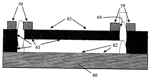
It is very important to observe the surface properties of the channel after
the
fabrication process, which is schematically described in Figure 7B. Indeed,
inside
the microchannel, the surface 6I is charged and hence hydrophilic, which is
necessary to enable capillary and/or electroosmotic flow. The wall of the
sealed
micro-channel made of the laminated layer 61 is yet less hydrophilic due to
the
nature of PE. Outside of the capillary, the surface 63 must be hydrophobic, so
as to
avoid the dispersion of the drop of solution around the openings serving as
inlet and
outlet. In the below examples, polyimide, which is an hydrophobic material, is
chosen for that purpose, since it becomes hydrophilic upon exposition to the
oxygen
plasma. Another surface property is the conductivity of the surface 64 where
the
metallic layer is in contact with the solution. These structures therefore
demonstrate
the concept of the invention: pattering different surface properties that are
needed for
controlling of the fluid flows, performing chemical reactions, detecting
analytes and
so forth.
CA 02399027 2002-07-31
WO 01/56771 PCT/CHO1/00070
- 25 -
Figure 7C shows another example of distribution of the above surface
properties,
where electrodes are placed directly above the inlet and outlet of a sealed
micro-
channel.
Next, the electrochemical detection is performed by cyclic voltammetry with an
AEW2 portable potentiostat (Sycopel Scientific, UK) by connecting one of the
electrodes as working electrode (WE) and another one as counter electrode
(CE). A
freshly oxidised Ag;AgCl wire is used as reference electrode and placed on the
top of
one channel entrance in contact with the solution to be analysed. Cyclic
voltammetry
characterisation of ferrocene carboxylic acid is first presented to understand
the
behaviour of the gold coated microelectrodes similarly to what was presented
earlier
in a previous paper.
Now, micro-structures fabricated according to the present invention are then
used to
demonstrate some examples of analytical applications, namely immunological
assays
and enzymatic reactions.
For the example of immunoassay, the immobilisation of the mouse antibodies was
performed by physisorption at pH 7 during one hour at room temperature.
Depending
on the experiments, between 1 and 100 p.g/ml of antibody concentration is
used. The
surface is then blocked with 5% $ovine Serum Albumin (BSA). The
immunoreaction is performed by filling dried channels with immobilised mouse
antibody with a goat antimouse-HRP conjugate and incubating it 5 minutes at
dilutions between 11225'000 and 1/25'000 titre. After the incubation with the
conjugate, the substrate solution containing 100 mM Hydroquinone and 100 mM
peroxyde is added to the channel to allow the electrochemical detection of
Horse-
CA 02399027 2002-07-31
WO 01/56771 PCT/CHO1/00070
-26-
Raddish-Peroxidase (HRP) with a similar procedure as that proposed by Wang et
al.
Between each step, a washing procedure is performed with a solution of washing
buffer at pH 7.4 and containg 0.1 M phosphate buffer and 0.1 % BSA.
In a second example, the use of the microchip is demonstrated for an enzymatic
assay. Plasma etched micro-structures have been used here for the detection of
glucose. A solution of Glucose oxidase (enzyme) and ferrocene carboxylic acid
(mediator) is mixed with a solution of glucose and filled in the microchannel
where a
cyclic voltammetric detection is performed.
In another schema, the Glucose oxidase and ferrocene solution is filled into
the
micro-channel, and the glucose solution is placed on one of the reservoirs.
In a further example, 2 p,L of glucose oxidase and ferrocene carboxylic acid
is
deposited and let dried on the electrode pads outside of the channel. Then a
solution
of glucose is deposited on the dried solution and a cyclic voltammetry is
performed.
In the following, the obtained results are shortly described.
First, the aspect of the structures used is addressed. Microscopy examination
of the
plasma etched plastic foils 70 before sealing by lamination of a PET-PE layer
shows
the different patterns that compose the micro-structure. Four top views of the
device
are presented in Figure 8, which contains a yellow-brown colour due to the
light
absorption of the polyimide layer 70. In the upper view on the left, the
presence of
the micro-channel 71 is shown as a hell pattern in the middle of the image,
meaning
that the thickness of polyimide at this place is smaller. At both ends of the
channel,
CA 02399027 2002-07-31
WO 01/56771 PCT/CHO1/00070
-27-
there is a hole 72 that serves as reservoir or as inlet and outlet, thereby
allowing to
access the liquid inside the channel after the lamination procedure. The other
lines
patterned on the surface 73 are the gold coated pads to connect the electrodes
with
the potentiostat. In the closer views of the device presented in »igure 8, it
can been
observed that the geometry of the electrode is a disk that is slightly
recessed from the
channel level.
It is worth noting that the upper view an the left side of Figure 8 also shows
series of
four holes 74 that are used for the precise alignment of the device during its
fabrication process.
Electrochemical characterisation: The cyclic voltammetric analyses of
ferrocene
carboxylic acid presented in Figure 9 exhibits an expected shape for
microelectrodes
of these dimensions in a microchannel.
A calibration of ferrocene carboxylic acid can be obtained between 0 and 0.5
mM
with a slope of 34 pA/qM, which is about 6 times larger than what was obtained
in
a similar geometry with a 5 times smaller carbon band electrode. The
performance of
these electrodes are in good agreement with such earlier work and can be used
for
diagnostics assays.
Glucose detection with plasma etched microchips: In a first experiment, the
reaction
is performed by mixing the enzyme and the mediator solution with a 15 mM
glucose
solution in a test tube outside the microchip. This solution is then injected
in the
microchannel and a cyclic voltammetry experiment is performed. The detection
of
glucose in such microchip can be shown in Figure 10. Without the presence of
glucose in the solution, the voltammogram shows the oxidation of ferrocene
CA 02399027 2002-07-31
WO 01/56771 PCT/CHO1/00070
-28-
carboxylic acid as in Figure 9. The presence of glucose is revealed by the
catalytic
shape of the voltammogram, meaning that the mediator is reduced and oxidised
by
the enzyme and the electrode respectively. This shows that the detection of
glucose is
possible within this microehannel. It is worth adding that the volume of the
micro
s channel is about 50 nL in this example.
In a second experiment, the glucose oxidase and ferrocene carboxylic acid
solution is
filled in the microchannel. Solutions of different concentrations of glucose
are then
deposited on the reservoir at the outlet of the microchannel. The glucose is
finally
detected by cyclic voltammetry as presented in Figure 11A. The current
detected at
400 mV is also plotted in Figure 11B against the glucose concentration. A good
correlation of the glucose concentration and the detected current is evidenced
between 0 and 20 mM. For larger glucose concentrations, the detection reaches
a
saturation.
In a third experiment, 2 ~,I, glucose oxidase and ferrocene carboxylic acid is
dried on
the electrode pads outside of the microchannel. In this experiment, 2 ~,L
solution of
glucose is added on the electrode pads and the recorded voltammograms are
presented in Figure 12A. The correlation of the current versus the
concentration
(Figure 12B) is linear from 0 to 20 mM. It is interesting to compare the
current
intensities between the detection inside the microchannel (Figures 10 and 11)
and on
the electrode pads outside of the microchannel. The current is larger in this
last
experiment because of the difference in the electrode dimension. The volume of
detection in this last case is Z ~,L versus 50 nL inside the microchannel.
Another example of application is now shown to demonstrate that the present
invention can be used to manufacture micro-structures in which the walls are
CA 02399027 2002-07-31
WO 01/56771 PCT/CHO1/00070
-29-
hydrophilic enough to generate a capillary flow and to control the movement of
the
fluids by electrical means. To this aim, the device schematically presented in
Figure
13 has been produced in a 50 ~,m thick polyimide foil 75 following an etching
process similar to that described in Figure 6. The device of Figure 13
contains a 10
cm long micro-channel 76 with one inlet 77 and one outlet 78 at each
extremity.
These inlet and outlet also serve as reservoirs, and they are surrounded by
two gold
coated copper pads 79 and 80 that are used as electrodes. In the outlet
reservoir, a
platinum electrode 81 and a silver/silverchloride (Ag/AgCI) reference
electrode 82
are put in contact with'the solution. A high electric field (1100 Volt) is
then applied
between electrodes 79 and 81, so as to electrokinetically pump the solution
through
the micro-channel 76 towards the outlet 78. The arrow in Figure 13 shows the
direction of the flow generated by the application of this high voltage. A low
potential (for example 400 mV vs Ag/AgCI) can also be applied between
electrodes
80 and 82 in order to detect the molecules reaching the outlet reservoir.
Preliminary experiments showed that it is possible to aspirate solution
through such
microchannels in order to fill and empty them easily. Further experiments have
then
been undertaken for the characterisation of the electroosmotic flow generated
in
sealed microchannels of the shape shown in Figure 13.
To this aim, a solution of ferrocene carboxylic acid (1 mM of ferrocene
carboxylic
acid in 10 mM phosphate buffer at pH 7.4) is placed at the inlet of the
microchannel
and pumped in the direction of the low voltage detection set-up placed at the
outlet.
As soon as the pumped electroactive species reach the outlet of the
microchannel, a
current is detected by the electrochemical system defined by electrodes 80 and
82.
As shown in Figure 14, when the solution only contains the phosphate buffer,
the
current remains close to zero. A current is only detected at the beginning of
the
experiment, which is an artefact due to the switching of the potential. When
the
CA 02399027 2002-07-31
WO 01/56771 PCT/CHO1/00070
-30-
ferrocene carboxylic acid solution is added at the inlet of the micro-channel,
the
current remains the same as that recorded for the phosphate buffer during 150
seconds. After these 150 seconds, the current rapidly increases until it
reaches a
plateau after approximately 200 seconds. This clearly shows that the ferrocene
carboxilic~ acid has been electrokinetically pumped through the micro-channel,
and
that it needed approximately 150 seconds to reaach the outlet reservoir.
This experiment demonstrates that it is possible to use electxoosmotic flow in
micro-
systems produced by the present invention and hence to use them to perform
electrophoretic separations as a chromatographic technique.
The three experiments shown here evidence the great interest of using the
present
structure or kind of structures fabricated by plasma etching for applications
in
chemical or biological analysis.
Enzyme linked immunosorberit assay (ELISA) with electrochemical detection: In
order to develop an immuno-diagnostic assay, antibodies can be immobilised on
the
T5 surface of the channel walls. The procedure ~ is performed on the basis of
physisorption or by covalent attachment. Then, standard immunoassay in
sandwich
or competitive mode can be performed. The detection can be achieved for
example
by having labeled the secondary antibody or the antigen with an enzyme such as
but
not limited to HRP, ALP, glucose oxydase, beta-galactosidase, etc. Structures
and
arrays or networks of structures similar to those shown in Figures 6 to 8 can
then be
used for such immunoassays, since appropriate surface properties can be
patterned
using the present invention.
CA 02399027 2002-07-31
WO 01/56771 PCT/CHO1/00070
-31-
Nanospray fabrication: The structure fabricated and presented in Figure 7 can
be
used for mass spectrometry analysis. Indeed, if the structure are cut either
with a
knife, a laser or by plasma, the cross section of the channel can be placed in
front of
a mass spectrometer inlet, and the high voltage required to spray the solution
out of
the capillary can be applied thank to the electrode fabricated inside the
capillary. The
interior of the channel (that is hydrophilic) serves to let the channel be
filled and the
outlet of the channel (that is hydrophobic) serves to favor the fabrication of
the
Taylor cone. Indeed, the exterior must be hydrophobic to prevent the aqueous
solution to spread outside of the channel, thereby favoring the generation of
the
spray.
These examples demonstrate the use of the present invention even if it is not
limited
to these applications.