Note: Descriptions are shown in the official language in which they were submitted.
CA 02399075 2003-08-26
METHOD AND APPARATUS FOR ADJUSTMENT OF THE SAMPLING
PHASE IN A PCM MODEM SYSTEM USING A DUAL-PHASE
PROBING SIGNAL
FIELD OF INVENTION
This invention relates to telecommunications and more particularly a method
and apparatus for optimizing the sampling phase in a PCM modem system.
BACKGROUND OF THE INVENTION
In order to transmit high-speed data in the upstream direction of a Public
Switched Telephone Network, PSTN, using an ITU-V.92 like PCM modem
connection it is necessary for a pre-equalizer to be employed by the analog
modem
transmitter to compensate for local loop channel distortion. It is known that
the
fractional sampling phase offset of the received symbol stream relative to the
A/D
quantizer at the central office, or CO, can have a significant effect on the
performance
of a pre-equalizer when the sampling rate is below the Nyquist rate. The
effect can be
large for symbol spaced pre-equalizers operating on received analog signals
with
significant excess bandwidth. Because the network sampling rate is fixed at 8
kHz, a
digital modem operating on the network employing a PCM upstream modulation
scheme would fall into this category.
For any particular equalization method and modulation scheme employed, it
can be determined, either through experimentation or analysis, which
fractional
symbol phase offset at the analog modem will yield the best performance. Since
the
initial phase of the received signal is determined by the random call timing
of the
analog modem and the loop channel, it is desirable for digital modem to have
the
ability to adjust the sampling phase of its quantizer relative to the received
signal.
1
CA 02399075 2003-08-26
However, the codec to which the digital modem is connected is remote from
the digital modem and is not under its control. It is thus not possible for
the digital
modem to adjust the sampling phase of the upstream quantizer at the codec. It
is
therefore necessary to have a method by which the digital modem can direct the
analog
modem to adjust the phase of its transmitted signal such that it hits the
codec at the
optimum instant.
By way of further background, in the case of a typical PCM modem system
there is an analog modem coupled over an analog link to a central office or
CO, at
which the analog signals are quantized and coupled to a digital modem. In the
analog
modem, a digital-to-analog converter is utilized to convert an incoming
digital data
stream to be transformed into an analog signal which is coupled via a hybrid
circuit to
a local analog loop. A node of the local analog loop is coupled to a central
office
which includes a codec and more importantly, a quantizer having both an
analog-to-digital converter and a digital-to-analog converter, with these
converters
being utilized to connect the digital network to the analog loop.
As described in a paper by J. E. Mazo, entitled Optimum Timing Phase for an
Infinite Equalizer, The Bell System Technical Journal, vol. 54, no. 1, January
1975, a
system is described for optiinizing the phase of a digital data stream or
transmission, in
which the phase refers to the phase of the samples. In this early paper, a
digital
equalizer is utilized to combine a sequence of the samples of the received
data wave,
with the equalizer being utilized to mitigate the effects of intersymbol
interference and
noise.
From this early work by J.E. Mazo, the phase of the sample point referenced to
the sampling interval is adjusted at the receiver by adjusting the phase of
the clock at
the receiver which drives the analog-to-digital converter used to convert an
incoming
analog stream into a digital equivalent. As described in this paper, a
different phase for
2
CA 02399075 2003-08-26
the sampling point yields different performances for the communications
system. J. E.
Mazo describes how to find the optimal sampling phase and calculates the
optimal
sampling phase by looking at the entire frequency spectrum.
While such an optimization technique is useful when one has control of the
analog-to-digital converter at the receiver, and more importantly the clock
driving the
A/D converter, in a PCM inodem system the analog-to-digital converter is
located at
the central office or CO. It will be appreciated that the CO is quite far
removed from
the digital modem, which is the ultimate termination point for the
transmission from
the analog-to-digital converter. There is thus no ability to be able to
remotely set the
clock frequency and phase of the clock at the CO, thereby precluding the
opportunity
to utilize the J.E. Mazo optimization system for optimizing channel
performance.
What will be apparent is that there is a requirement in PCM modem systems to
be able either to adjust the frequency and phase of the clock at the CO in
order to
improve performance, or to be able to adjust the sampling phase at the analog
modem
to be able to optimize the system for channel interference and noise.
SUMMARY OF THE INVENTION
In the subject system a method is provided which allows a digital modem,
during the initial training sequence, to adjust the sampling phase at the
analog modem.
This improves the performance of the pre-equalizer employed during data mode,
which translates into lower error rates, and/or higher connect speeds.
Generally, this method can be described in the following steps. First, it is
necessary for the analog modem to employ some sort of loop-back timing to lock
its
transmitter frequency to the network clock. After this frequency lock has been
established, the digital modem can use the received quantized samples of a
known dual
phase analog probing signal transmitted by the analog modem to compute a phase
3
CA 02399075 2003-08-26
estimate. This estimate is then compared to an optimum value and a sampling
phase
delay is computed which when employed at the analog modem shifts the
fractional
sampling phase offset to the optimum value at the CO. Note that this phase
delay need
only take on values between (0,1) with units of 1 symbol baud (1/8000 sec).
The digital modem encodes the required delay in the same manner it transmits
other parameters to the analog modem during training. After transmission of
the
required delay by the digital modem and decoding of this delay by the analog
modem,
the analog modem delays the input data stream by the required delay. This can
be
accomplished through a hardware adjustment of its codec or through software
methods
such as interpolation. After this adjustment, the received analog signal will
hit the
network codec at the central office at the phase desired by the digital modem.
Since it is necessary for the analog modem to employ some sort of loop-back
timing based on the network clock, a system such as described in U.S. Patent
5,199,046 by F. Ling may be used. This phase adjustment will be maintained
through
the entire connection. How the appropriate delay is generated is now
described.
While it is desirable to be able to adjust the phase and frequency of the
clock
which drives the digital-to-analog converter at the analog modem, in a
preferred
embodiment phase delay is accomplished by an interpolation of the digital data
stream
ahead of the digital-to-analog converter.
What sampling phase adjustment should be employed by the interpolation
requires some detection of the communications channel. In the subject
invention, the
optimal sampling phase delay is determined at the digital modem through the
utilization of the dual phase probing signal which is transmitted from the
analog
modem to the digital modem. The phase difference between the two phases of the
4kHz probing signal is set, in one embodiment, to 7z/2, which corresponds to
'/z with
units of 1 symbol baud (1/8000 see). Thus the second transmitted phase +2, is
4
CA 02399075 2003-08-26
determined by subtracting ir/2 from the first transmitted phase +1. This
relationship
between the phases is maintained at the receiver. Therefore, the second
received phase
~B at the digital modem is the same as subtracting 7c/2 from the first
received phase, ~A.
At the receiver, ~A is derived as the arctan of the summation of a ratio of
the
received signal with the first phase to the received signal with the second
phase, e.g.
~A=arctan 1/N E -sn,Z
S2(n)
Note that the above equation is valid when the sampling clock is twice the
probing tone and the phase difference is 7r/2.
In operation, the probing signal is sent in two segments, the first with the
first
phase and the second with the second phase. The received signal with both
phases are
collected and used by the phase detector to detect +A. The first and second
segments of
the probing signal in one embodiment are sampled at the 8 kHz network clock
rate.
With the sampling rate being 8 kHz, the probing signal in one embodiment is
set to 4 kHz. The received phase at the codec of the probing signal +A is
detected at the
digital modem and the optimal sampling phase is calculated. The optimal
sampling
phase is that which results in a fractional sampling phase offset of zero or n
at the CO.
This results in a maximum amplitude of the 4 kHz tone and thus optimum
performance
of the system.
Thus in one embodiment, the analog modem transmitter first sends a 4 kHz
tone with phase +1 followed by a second transmission with phase +2, where $Z=
~1-7E/2.
The reason why the 4 kHz tone is so important is that at the receive side, or
more importantly at the CO, due to the analog-to-digital converter whose
sampling
frequency is below Nyquist rate, the digital signal is an aliased version of
the original
signal.
5
CA 02399075 2003-08-26
After the analog-to-digital converter, the components or portions of the
signal
due to the skirts of adjacent waveforms, P1 and P2, can either add or subtract
depending on the phase of the fractional sampling phase offset, and this
effect is called
aliasing. One achieves better performance if these two components add. By
making P1
and P2 add each other constructively at 4kHz, it is more likely P1 and P2 will
add each
to the other at other frequencies. The important point is to select the
optimal phase
offset at which these two components, P1 and P2, add.
As will be seen, by selecting the probing signal frequency to be 4 kHz and
setting the phase difference of the phases of the two tone segments to be R/2,
it will be
shown that the ratio of the received signal with the first phase to the
received signal
with the second phase yields the appropriate delay to be inserted at the
analog end. In
one embodiment,
~A=arctan -sl(n)
S2(n)
Since, S1(n)=Acos(7zn+~A)=A(-1)n cos~A and S2(n)= Acos(M+W= -A(-1)n sin~A. To
make the estimate more accurate, the ratio of s(n)s can be averaged over many
samples, and this yields,
~A =arctan 1 /N Y =s,Un
s2(n)
where N is the number of received signal samples used to estimate phase ~A.
From the detection. of $A at the digital modem, one can calculate the optimal
delay that the analog modem must insert to make the new phase of the received
signal
zero or 7z, which is optimal. By inserting the appropriate delay, one sets the
sampling
phase at the analog side such that the two components P 1 and P2 add as
opposed to
subtract, which in turn yields optimal performance. From the above equations,
and
assuming the transmitter is currently transmitting at the ~2 phase, it can be
shown that,
the optimal delay D=(27r-$B)/(27r) mod 1=(2n+7c/2-W/(27c) mod 1.
6
CA 02399075 2003-08-26
In summary, in a PCM modem system, a method and apparatus for optimizing
the fractional sampling phase offset to maximize the upstream data rate
utilizes a
probing signal from the analog modem generated during startup and having two
or
more distinct phases, with the probing signal being detected at the digital
modem
where an optimum sampling phase is calculated. Thereafter an optimal delay is
calculated and is transmitted back to the analog modem where incoming data
symbols
are delayed by this amount. This makes the fractional sampling phase offset to
be
optimal at the central office quantizer.
More particularly, during startup the optimal sampling phase is determined by
transmitting a probing signal having two different phases of a known phase
difference
and determining from the ratio of the two received signals the optimal
sampling phase.
The optimal sampling phase delay in one embodiment is the arctan of the ratio
of the
two received probing signal segments. The arctan is calculated from measuring
the
received segments and is utilized to specify the optimal sampling phase delay
correction to be transmitted back to the analog modem.
Utilization of the two-phase 4 kHz tone permits one to assure that the
components at the sampling point will be additive given the insertion of the
correct
sampling phase delay. Since additive, the calculated sampling phase delay,
when
applied at the analog modem, will make the fractional sampling phase offset
optimal
when the transmitted signals arrive at the central office. This yields a
maximum
amplitude of the 4 kHz tone, thus indicating that the system has been set for
optimal
performance.
7
CA 02399075 2003-08-26
BRIEF DESCRIPTION OF THE DRAWINGS
These and other features of the subject invention will be better understood in
connection with the Detailed Description in conjunction with the Drawings; of
which:
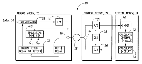
Figure 1 is a block diagram of a typical PCM modem system in which the
clock at the central office is locked to the network clock of 8 kHz and in
which the
clock at the analog modem is likewise locked to the network clock, in which
the
sampling phase offset of the signal at the central office quantizer has a
direct effect on
upstream data speed;
Figure 2A is a block diagram of a scenario in which digital data at the
transmit
side is sampled and converted to an analog signal transmitted through a
communications channel to a receiver having an analog-to-digital converter, in
which
the phase of the clock utilized for the analog-to-digital converter is
adjusted in an
optimal manner to provide for optimum sampling of the received analog signal;
Figure 2B is a waveform diagram illustrating the fractional sampling phase
offset of the analog signal which arrives at the receiver of Figure 2A;
Figure 3 is a block diagram of the subject system illustrating the
transmission
of a pure probing tone to permit calculating the delay to be transmitted back
to the
analog modem for delaying the incoming data stream to alter the sampling phase
such
that the sampling phase offset at the central office is optimum;
Figure 4A is a waveform diagram of the two segments of the probing signal
illustrating ax/2 phase shift between the two;
Figure 4B is a waveform diagram illustrating the segmented probing signal;
Figure 5A is a graph of amplitude vs frequency for the analog signal arriving
at
the central office, illustrating excess bandwidth;
Figure 5B is a graph of amplitude vs frequency of the sampled analog signal at
the central office illustrating aliasing;
8
CA 02399075 2003-08-26
Figure 6 is a diagrammatic representation of the detection of the phase of the
two segments of the probing signal, with the detected phase one of the
segmented
probing signals providing for calculation of the delay to be inserted to
adjust the
sample phase offset; and,
Figure 7 is a diagra2nmatic representation of another embodiment of the
subject
invention.
DETAILED DESCRIPTION
Referring now to Figure 1, a typical PCM modem system 10 includes an
analog modem 12 and a digital modem 14. In the upstream direction, the analog
modem is coupled via hybrid circuit 16 to a local analog loop 18, which is in
turn
connected through a hybrid circuit 20 in central office 22 to an analog-to-
digital
converter 24, in turn coupled to digital modem 14. Also at the central office
is a
digital-to-analog converter 26 in the downstream path, with a clock 28
utilized by both
the analog-to-digital converter and the digital-to-analog converter. It will
be
appreciated that analog-to-digital converter 24 functions as a quantizer. Note
that clock
28 is set at f0=8 kHz which is the network timing frequency.
The digital data 30 is generated by a pre-equalizer system. Analog modem 12
converts digital data 30 to an analog stream through the utilization of a
digital-to-analog converter 32. Digital-to-analog converter 32 is clocked via
clock 34
within the analog modem, which is locked to network timing such that fo is set
to 8
kHz through loop-back timing technology. Network timing is detected at the
analog
modem through the utilization of analog-to-digital converter 36 and/or a
downstream
receiver coupled to a timing detector 38 which is utilized at unit 40 to lock
clock 34 to
network timing.
9
CA 02399075 2003-08-26
While such a PCM modem system operates satisfactorily when the sampling
rate of digital data 30 is above the Nyquist rate, when the rate of data 30
and therefore
D/A converter 32 rate is below the Nyquist rate, such as 8kHz, to reduce the
complexity of the modem transmitter, modem speed must be reduced for robust
communications. The lost data is in part due to varying channel
characteristics
depending on the sampling phases.
As described in the above-mentioned paper by J. E. Mazo, a system can be
devised for optimizing the phase of a digital data stream or transmission, in
which the
phase refers to the phase of the samples. In the system envisioned by J. E.
Mazo, a
transmitter 40 accepts a digital data stream which is converted by a digital-
to-analog
converter 42 and coupled via a channel 46 to a receiver 48 .
Receiver 48 utilizes an analog-to-digital converter 50 coupled to channel 46
to
convert the incoming analog signal to a digital signal, with the output of A/D
converter
50 connected to an equalizer 52 and thence to a threshold device 54, with the
output of
the threshold device being the recovered digital data stream.
As will be appreciated, the sampling provided by analog-to-digital converter
50
is controlled by a clock 56 to adjust sampling phase offset as illustrated at
58 so as to
provide optimal performance for the system. According to the above-mentioned
paper,
the entire frequency spectrum is analyzed and an optimal phase offset
adjustment is
made at 58 to adjust clock 56.
Referring now to Figure 2B, analog waveform 60 is sampled at time T1, 2T,,
3T,, with the sampling interval T, being greater than the Nyquist interval
which is
defined as the inverse of Nyquist frequency. Note that by definition, sample
phase ~ is
the difference in time between 0 and the leading edge of the actual sample
pulse. Since
the sampling rate in the subject case is below the Nyquist rate, the sampling
phase is
critical.
CA 02399075 2003-08-26
As described hereinbefore, the scheme suggested in Figure 2A is impractical
because the digital modem does not have control of the central office analog-
to-digital
converter that is part of the quantizer because it is remote from the central
office. The
problem therefore becomes how the sampling phase offset can be adjusted.
In order to be able to provide an optimal sampling phase offset for the analog
signals arriving at the central office, in the subject system a probing signal
is generated
by the analog modem. This probing signal in one embodiment is a pure 4 kHz
tone
that has two segments. The phase shift between the two segments in one
embodiment
is 7[/2. This dual-phase signal is generated at 66 in the analog modem, with
the tone
injected between digital-to-analog converter 32 and hybrid circuit 16.
It is the dual-phase probing signal that is utilized at the digital modem to
be
able to calculate a phase delay which is to be inserted into data stream 30 by
an
interpolator 68 such that the signals arriving at the central office with an
optimal
fractional phase offset of zero or 7z.
In essence what is accomplished through the delay of the data stream ahead of
analog-to-digital converter 32 is to simulate a change in the phase of clock
28 at the
central office which would optimize quantizer sampling.
Note that in one operational embodiment, the probing signal is utilized in the
training phase of the PCM modem system and is transmitted at least initially
during
the startup mode. The incoming probing signal is converted from its analog
format to a
digital format and is coupled to a phase detector 70 which resides at the
digital
modem. The detected phase of one of the segments of the dual-phase probing
signal is
utilized at 72 to calculate an optimal sampling phase value, which in turn is
used at 74
to calculate the appropriate delay. This delay is the delay which is to be
inserted into
data stream 30 to correct for channel variations by providing an optimal
sampling
phase offset in the upstream direction.
11
CA 02399075 2003-08-26
The delay transmitted from the digital modem is detected at 76 at the analog
modem, with unit 78 driving interpolator 68 to insert a fixed delay to alter
the
sampling phase by the amount specified at the digital modem. In so doing, the
fractional sampling phase offset for analog signals arriving at the central
office is
adjusted to zero or 7E, thereby optimizing the system.
As to the probing signal, and as illustrated at Figure 4A, waveforms 80 and 82
represent ~, and +2 which are offset by 7r/2. As illustrated in Figure 4B,
waveform 80,
which has a phase of ~, is transmitted sequentially before waveform 82 which
has a
phase of ~2.
In one embodiment, the probing signal is a pure 4 kHz tone, the importance of
which has to do with aliasing occasioned by sampling below the Nyquist rate
and is as
follows:
Referring now to Figure 5A, waveform 84 represents the received tone prior to
analog-to-digital conversion at the central office. A portion 86 of waveform
84 extends
beyond the 4 kHz frequency point, with portion 86 forming a skirt indicating
by
shaded area 88 what is known as excess bandwidth. Given the 8 kHz sampling
rate, the
4 kHz tone results in an excess bandwidth which is relatively small.
Referring now to Figure 5B, waveforms 90, 90' and 90". are the result of the
analog-to-digital conversion in which components or portions P, and P2 exist
due to
aliasing. It will be appreciated that better performance is achieved if these
components
are additive. After the analog-to-digital converter, the components or
portions of the
signal due to the skirts of adjacent waveforms, Pl and P2, can either add or
subtract
depending on the phase of the fractional sampling phase offset, and this
effect is called
aliasing. One achieves better performance if these two components add. By
making P 1
and P2 add each other constructively at 4kHz, it is more likely P1 and P2 will
add each
to the other at other frequencies. The important point is to select the
optimal phase
12
CA 02399075 2003-08-26
offset at which these two components, Pl and P2, add.
In order to do this, the phase of the two segments of the 4 kHz tone is
detected
at the digital modem. Having detected the phase of the probing signal at the
digital
modem, it is possible to calculate the sampling phase offset that will give
the optimal
sampling phase offset at the central office and thus the maximum amplitude of
the 4
kHz tone, the reason for the improved performance.
Referring now to Figure 6, the first +, segment of the probing signal, here
illustrated at 92, is detected. This segment is sampled at 8 kHz as
illustrated at 94,
which yields a detected phase of ~A at 96. Likewise the second of the segments
of the
probing signa198 having a phase $2 is sampled at 100 to yield the detected
phase of the
second sample, namely ~B as illustrated at 102. As can be seen from the
formulas in
Figure 6, the detected phase ~A is such that:
~A =arctan -sn,2
S2(n)
From ~A one can calculate the optimal delay that the analog modem must insert
to make +B equal to zero, assuming the transmitter is currently at the ~2. In
so doing,
one inserts a delay such that the fractional sampling offset is either zero or
7z. The
inserted delay, D, in the illustrated embodiment is (27c+7r/2-$A)/(27r) mod 1.
Fig. 7 shows an example of a probing signal that has two different phases in
4kHz. The signals S1 and S2 are a repetition of {A 0 A -A 0-A}, where A is
chosen
to meet a certain power constraint. The probing signal consists of two
frequency terms:
1.3kHz and 4kHz. The 1.3kHz tone is not used to find optimal phase, but it is
to
sustain a certain power at the receiver even though there is a deep null at
4kHz at the
channel response. S 1' is added to let the receiver detect the boundary
between one
phase and another, i.e. between S1 and S2. Note that there is a 0.5T gap
between S1'
and S2 to give a 7z/2 phase difference between S1 and S2. This can really be a
gap that
does not have any signal component; or S1' could be extended to cover the gap.
At the
13
CA 02399075 2003-08-26
receiver, the 4kHz component of S1 and S2 is used to detect optimal phase.
Note that
to make the calculations niore accurate S 1' and S2' can also be used together
with S 1
and S2. Note also that 1.3kHz component can be easily filtered out at the
receiver, so
that only the 4kHz tone is used to calculate optimal phase.
Having now described a few embodiments of the invention, and some
modifications and variations thereto, it should be apparent to those skilled
in the art
that the foregoing is merely illustrative and not limiting, having been
presented by the
way of example only. Numerous modifications and other embodiments are within
the
scope of one of ordinary skill in the art and are contemplated as falling
within the
scope of the invention as limited only by the appended claims and equivalents
thereto.
14